N A N O E X P R E S S
Open Access
The function of a 60-nm-thick AlN buffer layer in
n-ZnO/AlN/p-Si(111)
Wei Wang, Chao Chen, Guozhen Zhang, Ti Wang, Hao Wu
*, Yong Liu and Chang Liu
*Abstract
ZnO films were prepared on p-Si (111) substrates by using atomic layer deposition. High-resolution x-ray diffraction (XRD), scanning electron microscopy (SEM), x-ray photoelectron spectroscopy (XPS), photoluminescence (PL), and I-V measurements were carried out to characterize structural, electrical, and optical properties. After introducing a 60-nm-thick AlN buffer layer, the growth direction of the ZnO films was changed from [10] to [0002]. Meanwhile, the ZnO crystalline quality was significantly improved as verified by both XRD and PL analyses. It has been demonstrated that the reverse leakage current was greatly reduced with the AlN buffer layer. The valence band offsets have been determined to be 3.06, 2.95, and 0.83 eV for ZnO/Si, ZnO/AlN, and AlN/Si heterojunctions, respectively, and the band alignment of ZnO/Si heterojunction was modified to be 0.72 eV after introducing the AlN buffer layer. Our work offered a potential way to fabricate Si-based ultraviolet light-emitting diodes and improve the device performances.
Keywords:AlN buffer layer; Heterojunction; ALD; Band alignment
Background
Si is the most useful substrate due to its low cost and easy integration [1,2]. P-type Si has the prominent merits to make driving voltage of light-emitting diode (LED) lower and the cost of device less expensive [3]. Therefore, the Si-based LEDs possess great competitive-ness. Zinc oxide (ZnO) is of interest as a result of its po-tential applications in ultraviolet (UV) optoelectronic devices due to its wide band gap of approximately 3.4 eV at room temperature and high exciton binding energy of approximately 60 meV [4]. Moreover, ZnO is thermally and chemically stable in ambient air, highly transparent in the visible region (>85%) [5], resistant to be oxidized, easy to fabricate, and relatively cheap compared to other optoelectronic materials [6]. So far, a variety of tech-niques have been utilized to grow ZnO thin films, such as, sputtering [7], molecular beam epitaxy (MBE) [8], pulsed laser deposition [9], and chemical vapor depos-ition [10]. As a chemical vapor processing with accurate surface control and self-limiting, atomic layer deposition (ALD) can prepare thin films with high uniformities and low defect densities.
Because of the large mismatches of the lattice con-stants (15.4%) and thermal expansion coefficients (60%) between ZnO and Si [11] and the oxidation of Si surface, direct growth of ZnO on Si substrates resulted in amorphous or polycrystalline films [12]. Attempts have been made to solve this problem by inserting different buffer layers between ZnO and substrates, such as GaN [13] and Al2O3[14,15]. It is well know that in the system of n-ZnO/p-Si, electron and hole recombination takes place mainly in Si rather than in ZnO, leading to a diffi-cult application for lighting since Si has a narrow and in-direct band gap. Owing to the difference in band gaps between ZnO and Si that provides an effective electron injection from ZnO to p-Si and blocks the flow of holes from p-Si to ZnO [16], it is necessary to understand the physical properties of the ZnO/Si heterojunction, espe-cially the energy band alignment and interfacial micro-structure. Some researchers employed different dielectric buffer layers to study the band alignment of the ZnO/ p-Si heterojunction [16-18]. However, few reports men-tioned AlN buffer layers between ZnO and Si. AlN has the widest direct band gap (6.2 eV) among all III-nitride
* Correspondence:[email protected];[email protected] Key Laboratory of Artificial Micro- and Nano-structures of Ministry of Education, and School of Physics and Technology, Wuhan University, Wuhan 430072, People’s Republic of China
semiconductors [19] and is used as buffer layer to grow GaN due to its outstanding physical and chemical prop-erties including high insulating resistance, high stability in severe conditions, and high thermal conductivity [20].
In this work, AlN buffer layer was introduced and the valence band offset (VBO) of ZnO/Si heterojunction was modified from 3.06 to 3.78 eV while the VBO between AlN and Si substrate was 2.95 eV. It was reported that the presence of SiOx made the VBO between SiOx and Si to be 3.15 eV [17], and those of Al2O3and HfO2 be-tween ZnO and Si substrate made the VBOs to be 3.24 and 2.87 eV, respectively [16].
Comparing with (100)-ZnO, (002)-ZnO exhibits better thermal stability. Therefore, control of the growth direc-tion of ZnO is crucial. Pung et al. [21] have proved that the deposition temperature played an important role in preferential growth of ZnO films, but changing the growth direction of ZnO films by inserting different buf-fer layers was rarely studied. In the early work of our group, we have prepared n-type (100)-ZnO deposited on Si (111) substrates with and without an Al2O3 buffer layer by ALD [14]. Under the same growth conditions, the growth direction of ZnO films has changed from [100] to [002] after introducing AlN as the buffer. The crystallization of the ZnO films was clearly improved, and the leakage current was significantly reduced.
Methods
The p-Si (111) substrates used in this work were all dipped for 60 s in a dilute aqueous hydrofluoric acid so-lution (2% HF) for the removal of the native oxide. The wafers were then ultrasonically cleaned in acetone for 10 min to remove organic grease and rinsed with ethanol.
The AlN buffer layer was grown by MBE (SVTA 35 V-2). The growth temperature and Al source temperature were set at 800°C and 1260°C, respectively. Prior to the growth, the Si substrate was thermally cleaned at 850°C for 10 min. Subsequent nitridation was performed at 850°C for 10 min in a nitrogen atmosphere with a flow rate of 2.65 sccm under 500 W RF-plasma power. The growth time for AlN was 5 min.
ZnO films were then deposited on AlN buffer layer by ALD (Beneq TFS-200) at a temperature of 200°C. Di-ethyl zinc (DEZn) and deionized water (H2O) were used as the sources of zinc and oxygen, respectively. During the deposition, DEZn and H2O were alternately fed into the chamber by using nitrogen as the carrier gas. A purge process using nitrogen was also introduced to clean the redundant former precursor. Four thousand cycles were performed and the ZnO films were 600 nm thick as measured by ellipsometer (Alpha-SE, J.A. Woollam, Lincoln, USA). A comparison between two samples named as A (without AlN buffer layer) and B
(with an AlN buffer layer about 60 nm) was performed to assess the function of the buffer layer
High-resolution x-ray diffraction (HRXRD, Bede D1, Bede Scientific Instruments, Durham, England, UK) and scanning electron microscope (SEM, Hitachi S-4800, Hitachi, Tokyo, Japan) were used to study the crystalliza-tion and interfacial properties. Photoluminescence (PL, BITPE miniPL-5.5, Photon Systems, Covina, CA, USA) measurements were carried out to analyze the near-band-edge (NBE) and deep emissions of the ZnO films with or without the AlN buffer layer. The electrical mea-surements were carried out to compare the effects of the buffer layer. The energy band alignments of ZnO/Si het-erojunction with or without the AlN buffer layer were measured by x-ray photoelectron spectroscopy (XPS; Thermo Scientific ESCLAB 250Xi, Thermo Fisher Scien-tific, Waltham, MA, USA).
For the XPS experiments, seven samples were pre-pared, namely, (1) a clean Si substrate; (2) a 5 nm ZnO film on Si substrate; (3) a 600-nm-thick ZnO film grown on Si substrate; (4) a 5-nm-thick AlN film grown on Si substrate; (5) a 60-nm-thick AlN film grown on Si sub-strate; (6) a ZnO (5 nm)/AlN (60 nm) heterostructure grown on Si substrate; (7) a ZnO (600 nm)/AlN (60 nm) heterostructure grown on Si substrate. The 5-nm-thick AlN layer was grown by MBE with the same conditions mentioned above but the growth period was 30 s.
[image:2.595.306.539.526.704.2]Results and discussion
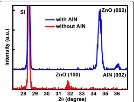
Figure 1 shows the XRD spectra of ZnO thin films grown by ALD without (sample A) and with the AlN buffer layer (sample B). For both samples, the diffraction peaks were all matched with the standard diffraction pattern of ZnO and AlN. As depicted in Figure 1, it was clearly seen that the thin AlN buffer layer played an
important role in determining the crystalline orientation of the ZnO thin films.
For sample A, the growth direction of ZnO film was [100], indicating the nonpolar nature of the ZnO films [14]. During the growth at 200°C, DEZn may dissociate into ethyl group fragments such as CH3 and these an-ions might adhere to the positively charged Zn-(002) polar surface [21,22]. Therefore, the growth direction of ZnO films was [100] on Si. On the other side, the lattice mismatch between AlN and ZnO was only 3.8% (calcu-lated from the powder diffraction file card 89–0510 and 89–3446 for ZnO and AlN, respectively), which was much less than that between ZnO and Si substrate. Thus, when the AlN buffer layer was introduced, the growth direction of ZnO films was kept along [002]. This is quite similar to what happened when InGaN buffer layer was introduced between ZnO and Si substrate [23].
Meanwhile, the intensity of ZnO (002) peak for sample B was much stronger than that of ZnO (100) peak for sample A. Considering that the ZnO films were depos-ited and tested under the identical conditions, it demon-strated that the AlN buffer layer forced ZnO films to grow along the c-axis.
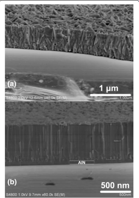
The cross-sectional SEM images of samples A and B are shown in Figure 2. The irregular cross profile of sample A revealed a polycrystalline nature of the ZnO film grown without any buffer layer on Si. Figure 2b shows that the AlN buffer layer was introduced be-tween the ZnO film and Si substrate, and the thickness of AlN buffer layer was measured to be 60 nm. It is ob-vious that the ZnO films in Figure 2b was regularly ori-ented while it was rambled in Figure 2a. The number of stacking faults and edge dislocations of sample B were obviously less than that of sample A. It can be con-cluded that with the AlN buffer layer, the crystalline quality of ZnO films was significantly improved.
[image:3.595.58.290.385.715.2]The room temperature PL spectra of ZnO thin films with and without the AlN buffer layer are shown in Figure 3. The main PL peaks at about 380 nm were due to the free excitation emission in ZnO, and a low en-ergy shoulder (at wavelength of 395 nm) was attribut-able to the emission related to point defects [24]. Usually, the ratio of band-edge transition (BET) to deep level emissions (DLEs) could evaluate the quality of ZnO films. It has been shown that the quality of ZnO films has been significantly improved after inserting the AlN buffer layer, because the ratio of BET to DLE of sample B (59.8) was larger than that of sample A (43.4). The DLE around 500 nm was caused by different in-trinsic defects in ZnO films such as oxygen vacancies and zinc interstitials [14]. The very weak DLEs of sam-ples A and B suggest that few zinc interstitials and few oxygen vacancies exist in the ZnO films, which can be attributed to the growth mechanism of ALD. The self-limiting aspect of ALD leads to a conformal depos-ition, because the precursors can adsorb and subse-quently desorb from the surface where the reaction has reached completion, and then proceed to react with
[image:3.595.305.538.518.695.2]Figure 2Cross-sectional SEM images of sample a and b.
other unreacted surface areas, while the redundant former precursor should be cleaned by the purge process. In this way, the two reactions (ZnOH* and Zn(CH2CH3) in this work) proceeded in a sequential fashion to deposit a thin film with atomic level control [25].
This can be further understood through the growth procedures of ALD as shown in the following reac-tions [21]:
ZnOHþZn CH 2CH3
ð Þ2→ZnOZn CHð 2CH3ÞþC2H6
Zn CHð 2CH3ÞþH2O→ZnOHþC2H6
Figure 4 shows a current–voltage (I to V) characteris-tic of the n-ZnO/AlN/p-Si heterostructure. The indium electrodes were welded on the surfaces of ZnO and Si layers to achieve the ohmic contacts. The ZnO films were etched to 1 mm × 1 mm by lithographic process to reduce contact resistance. The I to V curves were mea-sured by changing the bias voltage from +3 to−3 V. The current was restricted between 100 and −100 mA to protect the devices. Diode-like rectification behaviors were observed. Under the reverse bias of−2 V, the leak-age current of the n-ZnO/p-Si without the AlN buffer layer was about 94 mA (sample A) while that with the buffer (sample B) was about only 6 mA. Thus, the leak-age current has been effectively reduced due to the ex-cellent insulating property of the AlN buffer layer. Under the forward biases, the turn-on voltage of the sample A was about 0.47 V while it increased to about 1.25 V for sample B. The increase of the threshold volt-age was also due to the introduction of the insulating AlN buffer layer.
The energy band alignment of ZnO/Si and ZnO/AlN/ Si heterojunctions has been studied by using x-ray photoelectron spectroscopy (XPS). The VBO of ZnO/Si heterojunction can be calculated according to Kraut’s method [26] as follows:
ΔEZnO=Si
V ¼ ESiSi2s−E Si VBM
− EZnO Zn2p3=2−E
ZnO V BM
−ΔECL ð1Þ
ΔEAlN=ZnO
V ¼ EZnOZn2p3=2−EZnOVBM
− EAlN
Al2p3=2−EAlNVBM
−ΔECL1
ð2Þ
ΔEAlN=Si
V ¼ ESiSi2s−E Si VBM
− EAlN Al2p3=2−E
AlN VBM
−ΔECL2 ð3Þ
Where Esi denotes the energy for feature i in sample s, Zn 2p3/2, Al 2p3/2, and Si 2 s core levels (CLs) were used in Equations 1 to 3. The CL spectra were fitted by the
Voigt (mixed Gaussian-Lorentzian) line shape by
employing a Shirly background to determine the respect-ive CL positions.ΔECL,ΔECL1, andΔECL2were the en-ergy difference between the CLs of Zn 2p3/2 and Si 2 s,
Zn 2p3/2 and Al 2p3/2, and Si 2 s and Al 2p3/2,
respectively.
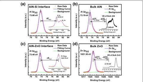
[image:4.595.60.538.495.703.2]The results of XPS measurements are shown in Figure 5 for ZnO/Si heterojunction and Figure 6 for ZnO/AlN/Si heterojunction. Figure 5a shows the VBM and the CL spectra of Si 2 s recorded on Si substrate. The VBM of bulk Si was determined to be 0.15 eV by linear extrapolation, and the Si 2 s peak was located at 150.18 eV corresponding to the Si-Si bond [16]. The Zn
2p3/2and Si 2 s spectra at the interface of ZnO/Si het-erojunction were presented in Figure 5b, and the peaks were located at 150.07 and 1022.26 eV, respectively. In the thick ZnO films, it can be seen from Figure 5c that the Zn 2p3/2CL peak was slightly shifted to 1021.54 eV, corresponding to the Zn-O bonding state [27]. At the
same time, the VBM of bulk ZnO was determined to be 2.38 eV. Thus, the ΔECL was calculated to be 872.19 eV. ΔEZnOV =Si was then calculated to be 3.06 eV using Equation 1.
Figure 6a shows the Al 2p3/2and Si 2 s spectra at the interface between AlN and Si. The Al 2p3/2 peak was located at 73.66 eV, corresponding to the Al-N bond [28]. Besides, the Si-Si bond at 149.95 eV, a significant peak appeared at 152.05 eV that can be attributed to the bonding configuration of Si-N [29]. This Si-N bond may originate from the nitridation process for the ini-tial Si substrate processing performed at 850°C, form-ing SiNx with an ultrathin thickness to be hardly measured. The VB and the CL spectra of Al 2p3/2 for the bulk AlN are displayed in Figure 6b. The VBM position and the Al 2p3/2CL peak were determined to be 2.40 and 73.19 eV, respectively. In the meanwhile, the VBM and the Zn 2p3/2CL were deduced to be 2.14 and 1021.38 eV for the bulk ZnO film with AlN buffer layer from the results shown in Figure 6d. Figure 6c shows the Al 2p3/2 and Zn 2p3/2 spectra at the inter-face of AlN/ZnO heterostructure. Compared to those of the bulk AlN and ZnO samples, the Al 2p3/2and Zn 2p3/2 peaks shifted to 73.48 and 1022.76 eV, respect-ively. With all the values obtained above, ΔEAlNV =ZnO and ΔEAlNV =Si were calculated to be −0.83 and 2.95 eV using Equations 2 and 3. Finally, the conduction band offset (ΔEC) at each interface can be estimated from the following formula:
ΔEZnO=Si
C ¼EZnOg −E Si g−ΔE
ZnO=Si
V ð4Þ
ΔEAlN=Si
C ¼EAlNg −E Si g−ΔE
AlN=Si
V ð5Þ
ΔEAlN=ZnO
C ¼EAlNg −E ZnO g −ΔE
AlN=Si
V ð6Þ
The band gap of bulk ZnO, Si, and AlN at room temperature was known to be 3.37 [30], 1.12 [31], and 6.2 eV [19], respectively. With the VBO values that have already been calculated, the conduction band offsets (CBOs) were found as follows:
ΔEZnO=Si
C ¼0:81 eV,ΔE AlN=Si
C ¼2:13 eV, andΔE AlN=ZnO
C ¼
3:66 eV.
The band alignment of two bi-interface systems is il-lustrated in Figure 7 which includes all energy levels.
[image:5.595.58.289.82.585.2]As shown in Figure 7, the introduction of an AlN buffer layer lead to changes of VBOs and CBOs be-tween ZnO and Si substrate. The presence of the AlN buffer layer can modify the band alignment between ZnO and Si to an extent as large as 0.72 eV. The VBO between AlN and Si substrate was smaller than that be-tween ZnO and Si substrate, which makes it easier to inject holes from Si to ZnO by means of AlN. The AlN Figure 5XPS narrow scans of ZnO/Si heterojunction. (a)XPS
buffer layer acted as a ladder. More importantly, those tunneled holes need only overcome a 0.83 eV barrier to enter into ZnO. On the other side, the CBO (as large as 3.66 eV) between AlN and ZnO can block the flow of electrons from ZnO to p-Si. Thus, electron–hole
recombination may mainly take place in the ZnO layer. A weak luminescence could be observed from the n-ZnO/AlN/p-Si heterojunction at room temperature when a positive voltage was applied to the p-Si sub-strate. However, more work need to be carried out to improve the luminous efficiency in the future.
Conclusions
In summary, we had prepared heterojunctions of ZnO films on Si (111) substrates by ALD. The 60-nm-thick AlN buffer layer was introduced to improve the crystal-line quality and change the growth direction of ZnO films from [100] to [002]. With the AlN buffer layers, the BET peak was enhanced while the DLE was still kept at a low level. The band alignment ZnO/Si hetero-junction was modified to be 0.72 eV after introducing the AlN buffer layer. The large CBO between AlN/Si heterojunction blocks the flow of electrons from ZnO to p-Si, while the decreased VBO makes it easier to in-ject holes from p-Si to ZnO
Competing interests
The authors declare that they have no competing interests.
Authors’contributions
[image:6.595.58.539.89.365.2]WW carried out the experiments and drafted the manuscript. HW conceived the study and participated in its design. CC and TW participated in the design of the study and performed the analysis. GZZ and YL participated in Figure 6XPS narrow scans of ZnO/AlN/Si heterojunction. (a)XPS narrow scans of Al 2p3/2 and Si 2 s at AlN/Si interface;(b)XPS narrow scans of Al 2p3/2 and VBM of bulk AlN;(c)XPS narrow scans of Al 2p3/2 and Zn 2p3/2 at ZnO/AlN interface;(d)XPS narrow scans of Zn 2p3/2 and VBM of bulk ZnO on an AlN buffer layer.
[image:6.595.56.291.510.705.2]the measurements. CL supervised the overall study. All authors read and approved the final manuscript.
Acknowledgements
This work is supported by the NSFC under Grant Nos. 11074192, 11175135, J1210061, Hubei Provincial Project 2012BAA19009 and the Fundamental Research Funds for the Central Universities (2014202020209). Dr. Wu is supported by China Scholarship Council No. 201208420584.
Received: 10 December 2014 Accepted: 9 February 2015
References
1. Jeong I-S, Kim JH, Im S. Ultraviolet-enhanced photodiode employing n-ZnO/p-Si structure. Appl Phys Lett. 2003;83:2946–8.
2. Chen P, Ma X, Yang D. Ultraviolet electroluminescence from ZnO∕p‐Si heterojunctions. J Appl Phys. 2007;101:053103.
3. Ye JD, Gu SL, Zhu SM, Liu W, Liu SM, Zhang R, et al. Electroluminescent and transport mechanisms of n-ZnO∕p-Si heterojunctions. Appl Phys Lett. 2006;88:182112.
4. Li XD, Chen TP, Liu P, Liu Y, Liu Z, Leong KC. A study on the evolution of dielectric function of ZnO thin films with decreasing film thickness. J Appl Phys. 2014;115:103512.
5. Periasamy C, Chakrabarti P. Large-area and nanoscale n-ZnO/p-Si heterojunction photodetectors. J Vac Sci Technol B. 2011;29:051206. 6. Ng S, Ooi P, Ching C, Hassan Z, Hassan HA, Abdullah M. Structural and
morphological properties of zinc oxide thin films grown on silicon substrates. In: AIP Conference Proceedings, vol. 1528. 2013. p. 306. 7. Sago K, Kuramochi H, Iigusa H, Utsumi K, Fujiwara H. Ellipsometry
characterization of polycrystalline ZnO layers with the modeling of carrier concentration gradient: Effects of grain boundary, humidity, and surface texture. J Appl Phys. 2014;115:133505.
8. Azarov AY, Hallén A, Du XL, Rauwel P, Kuznetsov AY, Svensson BG. Effect of implanted species on thermal evolution of ion-induced defects in ZnO. J Appl Phys. 2014;115:073512.
9. Lee J-C, Huang L-W, Hung D-S, Chiang T-H, Huang JCA, Liang J-Z, et al. Inverse spin Hall effect induced by spin pumping into semiconducting ZnO. Appl Phys Lett. 2014;104:052401.
10. Treharne RE, Phillips LJ, Durose K, Weerakkody A, Mitrovic IZ, Hall S. Non-parabolicity and band gap re-normalisation in Si doped ZnO. J Appl Phys. 2014;115:063505.
11. Iwata K, Fons P, Niki S, Yamada A, Matsubara K, Nakahara K, et al. ZnO growth on Si by radical source MBE. J Cryst Growth. 2000;214:50–4. 12. Hubbard K, Schlom D. Thermodynamic stability of binary oxides in contact
With silicon. J Mater Res. 1996;11:2757–76.
13. Nahhas A, Kim HK, Blachere J. Epitaxial growth of ZnO films on Si substrates using an epitaxial GaN buffer. Appl Phys Lett. 2001;78:1511–3.
14. Wang T, Wu H, Chen C, Liu C. Growth, optical, and electrical properties of nonpolar m-plane ZnO on p-Si substrates with Al2O3 buffer layers. Appl Phys Lett. 2012;100:011901.
15. Zhang L, Jiang H, Liu C, Dong J, Chow P. Annealing of Al2O3 thin films prepared by atomic layer deposition. J Phys D Appl Phys. 2007;40:3707. 16. Lu H-L, Yang M, Xie Z-Y, Geng Y, Zhang Y, Wang P-F, et al. Band alignment
and interfacial structure of ZnO/Si heterojunction with Al2O3 and HfO2 as interlayers. Appl Phys Lett. 2014;104:161602.
17. You JB, Zhang XW, Zhang SG, Tan HR, Ying J, Yin ZG, et al. Electroluminescence behavior of ZnO/Si heterojunctions: Energy band alignment and interfacial microstructure. J Appl Phys. 2010;107:083701. 18. Huang H, Fang G, Mo X, Long H, Wang H, Li S, et al. Improved and orange
emission from an n-ZnO/p-Si heterojunction light emitting device with NiO as the intermediate layer. Appl Phys Lett. 2012;101:223504.
19. Cheng B, Choi S, Northrup JE, Yang Z, Knollenberg C, Teepe M, et al. Enhanced vertical and lateral hole transport in high aluminum-containing AlGaN for deep ultraviolet light emitters. Appl Phys Lett. 2013;102:231106. 20. Fu Q, Peng T, Liu C. Effects of real-time monitored growth interrupt on
crystalline quality of AlN epilayer grown on sapphire by molecular beam epitaxy. J Cryst Growth. 2009;311:3553–6.
21. Pung S-Y, Choy K-L, Hou X, Shan C. Preferential growth of ZnO thin films by the atomic layer deposition technique. Nanotechnology. 2008;19:435609.
22. Cagin E, Yang J, Wang W, Phillips J, Hong S, Lee J, et al. Growth and structural properties of < equation > m</equation >−plane ZnO on MgO (001) by molecular beam epitaxy. Appl Phys Lett. 2008;92:233505. 23. Wang T, Wu H, Wang Z, Chen C, Liu C. Improvement of optical
performance of ZnO/GaN pn junctions with an InGaN interlayer. Appl Phys Lett. 2012;101:161905.
24. Liang Y-C. Growth and characterization of nonpolar < i > a</i >−plane ZnO films on perovskite oxides with thin homointerlayer. J Alloys Compd. 2010;508:158–61.
25. George SM. Atomic layer depositions: an overview. Chem Rev. 2009;110:111–31.
26. Kraut EA, Grant RW, Waldrop JR, Kowalczyk SP. Precise determination of the valence-band edge in x-ray photoemission spectra: Application to measurement of semiconductor interface potentials. Phys Rev Lett. 1980;44:1620–3.
27. You JB, Zhang XW, Song HP, Ying J, Guo Y, Yang AL, et al. Energy band alignment of SiO2/ZnO interface determined by x-ray photoelectron spectroscopy. J Appl Phys. 2009;106:043709.
28. Lu X, Ma J, Jiang H, Liu C, Lau KM. Low trap states in in situ SiNx/AlN/GaN metal-insulator-semiconductor structures grown by metal-organic chemical vapor deposition. Appl Phys Lett. 2014;105:102911.
29. Jiang X, Ma Z, Yang H, Yu J, Wang W, Zhang W, et al. Nanocrystalline Si pathway induced unipolar resistive switching behavior from annealed Si-rich SiNx/SiNy multilayers. J Appl Phys. 2014;116:123705.
30. Yang Z-G, Zhu L-P, Guo Y-M, Tian W, Ye Z-Z, Zhao B-H. Valence-band offset of p-NiO/n-ZnO heterojunction measured by X-ray photoelectron spectroscopy. Phys Lett A. 2011;375:1760–3.
31. Jia CH, Chen YH, Zhou XL, Yang AL, Zheng GL, Liu XL, et al. Valence band offset of ZnO/BaTiO3 heterojunction measured by x-ray photoelectron spectroscopy. Appl Phys A. 2010;99:511–4.
Submit your manuscript to a
journal and benefi t from:
7Convenient online submission
7Rigorous peer review
7Immediate publication on acceptance
7Open access: articles freely available online
7High visibility within the fi eld
7Retaining the copyright to your article