RECONFIGURABLE AND MODULAR BASED SYNTHESIS
OF CYCLIC DSP DATA FLOW GRAPHS
AWNI ITRADAT
Assistant Professor, Department of Computer Engineering,
Faculty of Engineering, Hashemite University, P.O. Box 150459, Zarqa 13115, Jordan E-mail: [email protected]
ABSTRACT
The conventional high level synthesis techniques target DSP algorithms onto architectures using basic functional units such as adders or multipliers. In this paper, a scheme for the partitioning of the data flow graph of a DSP application for a high-level synthesis aimed at a design using multi-modules is proposed. In the propose scheme, the regularity characteristics of DSP application are exploited. Moreover, in order to reduce the number of distinct modules, the near-isomorphism sub-graphs represents the modules are merged together by multiplexing them in time to produce a single adaptable module. This merging process enables the reuse of the adaptable modules by partially reconfiguring them at run time to realize different modules during the running of the DSP data flow graph. Furthermore, a novel reconfigurable multiplier multiplier is incorporated in the proposed synthesis technique. It is seen that a small overhead in terms of the architecture’s controller is needed by the modules in order for them to be adapted to perform different computations (multi-modes).
Keywords:Architectural Synthesis; Reconfigurable Multimodule; Time Scheduling, Reconfigurable Processing Units
1. INTRODUCTION
Some of the applications that need a high-level synthesis are digital signal processing (DSP), communications, and image processing. These applications are among the most important applications that demand high computational power, and must be executed at a very high speed to enable real-time processing. Due to the parallelism within the DSP applications, parallel processing architectures are a natural choice for the synthesis of these applications.
Moreover, the need to reduce the design time of digital systems, and thus, the time to market is increasingly crucial factor to have a competitive edge. Such an advantage can be achieved if there are efficient techniques to reduce the time taken by each of the individual steps of the design process. The design cycle of a digital system is composed of three major steps: RTL design, Physical implementation and Verification or Validation at various levels of design and implementation. A multi-module design could be an attractive platform to reduce the overall design time by reducing the time of the steps of the design cycle following the step at which the modularity is introduced. There exist a variety of architectural synthesis techniques, most of which target DSP algorithms onto multiprocessor architecture using basic functional
units such as adders or multipliers [1][2]. This however results in inferior implementation of DSP applications, since the regularity feature of DSP application are not exploited.
Furthermore, hardware flexibility is a crucial factor in today’s system design. However, such flexibility must not be gained at the expense of performance and area, as is the case with general-purpose reconfigurable fabrics such as field programmable gate-arrays (FPGAs) [3]. Hybrid FPGAs and reconfigurable cores provide hardware flexibility, their coarse integration of fixed logic and reconfigurable fabric results in performance, area and power penalties [4]. New techniques have therefore been explored to add flexibility to individual hardware components without the penalties associated with FPGAs. To overcome the latter penalties, small-scale reconfiguration would minimizes the area and delay penalties by inserting into fixed-logic only the minimum amount of reconfigurable logic and interconnect and by reusing the main part of the available logic and by changing the status of a few control signals to achieve the desired component functionality.
those near-isomorphism modules (sub-graphs) are merged together by multiplexing them on time. The original data flow graph (DFG) represents the DSP application is reconstructed by using the extracted and merged modules. Scheduling and allocation techniques are proposed to map the DSP application onto reconfigurable multi-module structure. The proposed architectural synthesis technique operating on the cyclic multi-module based DFG of a DSP algorithm is designed to determine the relative firing times of the nodes by using Floyd-Warshall's longest path algorithm [5] so that the throughput is aimed to be maximized and the number of distinct module resources is aimed to be minimized.
2. SCHEME FOR MULTI-MODULE SYNTHESIS
The data flow graph (DFG) is proven to be an efficient representation of the system specification due to its ability to expose the hidden concurrency between the operations of the underlying algorithm. Since DSP applications are known for their inherent parallelism, the DFG model is suitable for the DSP applications. Moreover, regularity is an inherent feature of several VLSI systems, especially those we find in signal processing applications. Data flow graph representations is an efficient to exploit such regular characteristics of such applications. Unfortunately, most of architectural synthesis algorithms proposed to-date aim to provide a generalized approach to synthesis, without usually much regard to the special characteristics of the system being synthesized. An efficient work on regularity extraction could be found in [6].
We present in this paper an approach to high-level synthesis (specifically, scheduling and module allocation) that is aimed to exploit the inherent characteristics of DSP circuits. We assume here that the designer has the behaviour of the filter in terms of its dataflow graph. We propose that such behavioural data-flow graphs can be abstracted as a collection of identical or near-identical modules (sub-graphs), each of which represents a part of the behaviour. The flow graph of these module is the one on which we perform the scheduling and module allocation. Thus, hardware sharing is now done on the module (sub-graph), rather than on individual functional units like adders and multipliers.
Once each of the module templates is fully characterized, we are left with the task of having to schedule the multi-module based graph.
The overall synthesis scheme involves the following steps.
1. Identification of common module structures: The computation module structures can be identified by using regularity extraction algorithm [6]. 2. Reconstruction of the data flow graph
representing the DSP application using the newly identified module structures. 3. Determination of the computational delay
of each module. This is done by the synthesis of the internal module computations.
4. Scheduling of the newly constructed cyclic data flow graph (the module-based DFG). 5. Allocation of modules onto multi-module
structures.
6. Synthesis of control structures: In this step the control signals specifies the data flow of the algorithm are retargeted for synthesising the base module structures.
3. TIME SCHEDULING AND ALLOCATION OF MULTI- MODULE FLOW GRAPH After the extraction of the regular modules of a DFG, this original DFG is reconstructed by clustering those computations having isomorphism with the extracted modules. Those computations which are not covered by any module because they don’t have an isomorphism with any extracted module are considered as if they are separate modules. A module-based graph G can be represented by the pair (M, E), where M is a set of nodes (modules), and E is a set of elements called edges. Each edge is associated with a pair of modules. The symbols m1,m2,...mn−1,mnare used to
represent the modules, and the symbolse1,e2,... are
used to represent the edges of a graph. A direct path
k m m
P0 is a finite sequence of distinct modules
k
m m
m0, 1,..., and distinct edges such that the edge
) ,
(mi mi+1 is present in the path
k
m m
P0 . If m =mk
0 then
this path is called a directed circuit or loop. Each loop in a DSP graph must contain at least one ideal delay element for the graph to be computable. The data flow graph that contains at least one directed circuit is called the cyclic graph, otherwise it is acyclic.
calculated. The module mobility is equal to the difference between its calculated latest and earliest firing times. These earliest and the latest firing times are found relative to a reference node. Given a module-based data flow graph of a DSP application, the time scheduling can be built using the longest path matrix f
Q [5]. The entries of this matrix represent the length of the longest path between each pair of modules (mimj) which is
given by [ [ max j i j m i m m m P all f
ij len P
Q = (1)
The earliest firing time and the latest firing time for a module mj relative to that of a reference
module mi are, respectively, given by
( )
f ij i m m Q m FT EFT ij = +
(2)
( )
f ji i m m Q m FT LFT ij = −
(3)
where FT
( )
mi is the firing time of modulei
m . To
find the earliest and the latest firing times of nodemi, the maximum earliest firing time and the
minimum latest firing time of the module must be found relative to all previously scheduled modules. Thus, EFT and LFT of node mj are, respectively,
given by = < ) ( ) max i j j m m EFT EFT(m j i all (4) = < ) ( ) min i j j m m LFT LFT(m j i all (5)
A valid schedule range specifies a valid way to schedule the module for a given the precedence relations. Thus, the mobility is given asM
( )
vj =LFT( )
mj −EFT( )
mj .3.1 The time schedule
The time schedule is built by selecting a reference-module and by calculating the mobility of all non-scheduled modules with respect to this reference module. All the non-scheduled modules are put in a list. The module with the minimum mobility calculated thus far is chosen for scheduling first and then removed from the list. When choosing between equal mobility modules, the selection is made such that individual modules concurrency is equalized with the previous step. This is to increase the probability that a module unit would be reused by dynamically reconfiguration a few control signals or even without any
reconfiguration. Due to the new firing time of the module, the time schedule of other non-scheduled modules may be affected. This module is chosen to be the new reference-module and the rest of all the earliest and latest firing times for the rest of the non-scheduled modules are calculated. A new module is chosen for scheduling and the process is iteratively repeated.
3.2 Choosing the firing time
We defined the level of a control step to be the number of modules which will eventually occupy this control step. This level determines the number of module structures required in the implementation of the final system. The chosen module is scheduled to fire at a control step that would results in a minimum number of functional modules required. We defined the level of a control step to be the summation of sub-levels of the different types of operations and given by
... 2
1+ +
=leveltype leveltype
level . The choosing of the best
firing time is done by examining all the control steps within its mobility such that total number of module per cycle is minimized, rather than individual module concurrency. More specifically, find the control step having the minimum total level as a primary key or the minimum sublevel (leveltype)
as a secondary key.
3.3 Scheduling algorithm
The scheduling algorithm involves the following steps.
Algorithm 1 Time schedule
1. Calculate the minimum iteration period. Find the longest path matrix.
2. Take the input module as the reference and schedule it first to fire at the control step zero.
3. Calculate the earliest and latest firing times of all the remaining modules with respect to the input module.
4. Calculate the current schedule range or mobility for each of the remaining non-scheduled modules.
6. Based on the current mobility for each non-scheduled module, choose one module as the target module for the scheduling according to the following priority:
a. A module that has the minimum current mobility. If more than one module has minimum current mobility, chose from these modules the one that is a predecessor or successor to the current reference module.
b. A module that is longest computational time and a predecessor or successor of any scheduled module. c. Any first available module.
7. Within the scheduling range of the target module, find the best firing time position as the control step that has the minimum level. If more than one control step results in the same minimum possible level, chose minimum sublevel. Set the best firing time position found as the time schedule of the target module.
9. Set the target module to be the new reference node. Update the earliest and latest firing times of all the remaining non-scheduled modules.
10. Go to Step 4 until all the modules have been scheduled.
3.4 Multi-module allocation
A straight forward allocating the modules in the data flow graph onto multi-module structure from a time schedule can be carried out by using an allocation algorithm similar to the one presented in [7].
4. MERGINGOFNEAR-ISOMORPHISM
MODULES
In order to reduce the number of distinct modules in the multi-module structure, the sub-graphs represent each selected module are merged together, synthesizing a single reconfigurable module structure for the near-isomorphism modules. The data-flow graph merging process enables the reuse of hardware blocks and interconnections by identifying similarities among the DFGs representing the modules, and produces a single module structure that can be partially reconfigured at run-time by setting some control signals specifically for each module (sub-graph).
Efficient merging techniques can be found in [8] and [9].
In addition to modularity, this merging process results in a data-path having a few and simple hardware blocks (module units and registers) and interconnections (multiplexers and wires), which in turn, reduces its cost, area, and power consumption. Achieving such an aim is possible if hardware blocks and interconnections be reused across the application as much as possible. The module allocation that is used in the previous section has also a great impact in reducing the system reconfiguration overhead, both in time and space. An example of module merging is shown in Fig. 1.
0
c
2 1
1
0 0
0 Merged G c Merged G
[image:4.595.305.512.295.372.2]c= → = = → =
Fig 1: Merging of two modules (sub-graphs)
5.EXAMPLES
In this section, we consider two examples of DSP filters, a fourth-order Jaumann filter and fourth-order lattice All-pole filter, in order to demonstrate the proposed synthesis scheme. In the two benchmark problems, the computational delays of the addition and multiplication nodes are assumed to be 1 and 5 cycles, respectively. Moreover, the delay of multiplexer is assumed to be equal to that of the adder, i.e., 1 cycle.
5.1 Fourth-order Jaumann wave filter
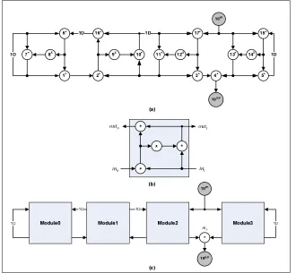
The DFG of the fourth-order Jaumann wave filter is shown in Fig. 2(a). Fig. 2(b) shows extracted regular module for this filter. A latency of 8 cycles for this module is calculated based on its critical path from input to output. The time schedule and module allocation obtained for the multi-module based DFG (Fig. 2(c)) by using the proposed technique are given in Fig. 3. It is seen, that the iteration period obtained for this filter using multi-module structure is 16 cycles which is equal to that using individual hardware functional units. Hence, modularity is gained without penalties in terms of delay or throughput.
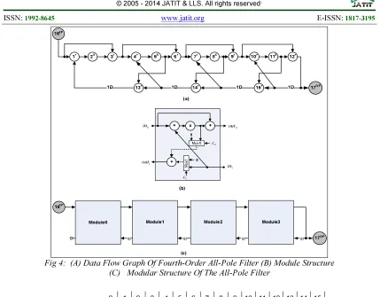
5.2 Fourth-order all-pole lattice filter
latency of 8 cycles for this module is calculated based on its critical path, i.e. (+, *, MUX, +). The time schedule and module allocation obtained for the multi-module based DFG are given in Fig. 5. Fig. 6 shows the status of the reconfiguration
control signals that are dynamically changed each iteration of execution. Fully-regular and reconfigurable multi-module structure is obtained, but associated with a penalty of 2 cycles in terms of iteration period.
0
out out1
1
in
0
in
4
m
Fig 2: (A) Data Flow Graph Of Fourth-Order Jaumann Wave Filter (B) Module Structure (C) Modular Structure Of The Jaumann Wave Filter
0 0
m
1 3
m
02
m
0 4
m
[image:5.595.135.465.199.504.2]0 1
m
[image:5.595.130.472.567.661.2]0 c
1 c 0
in
1
in 0
out
1
out
Fig 4: (A) Data Flow Graph Of Fourth-Order All-Pole Filter (B) Module Structure (C) Modular Structure Of The All-Pole Filter
0 0 m
1 3−
m
1 2−
m
[image:6.595.84.513.97.432.2]0 1 m
Fig 5: Time schedule of multi-module based fourth-order all-pole filter
0 0=
C
0 1=
C
1
0=
C
1 1=
C
1 0=
C
1 1=
C
1
0=
C
1
[image:6.595.170.451.424.489.2]1= C
Fig 6: Reconfiguration Control Signals Of Each Adaptable Module
6. INCORPORATIONOF
RECONFIGURABLEPROCESSINGUNIT
We incorporate dynamically reconfigurable functional units [10][11] in the extracted modules in order to increase regularity and optimize the area of each module.
The reconfigurable multiplier is employed in the proposed scheme since it is capable of implementing both multiplication and addition (in fact, it can perform two or more data-independent additions in parallel) with the same delay as a fixed
[image:6.595.148.453.513.582.2]0
c
0
c
(a)
0
c c0
(b)
[image:7.595.83.514.85.408.2]Fig 7: (A) A Module With Basic FU (B) A Module With Reconfigurable FU Incorporated
Fig 8: Iteration Period Obtained For DSP Applications Targeting Modular Architectures With And Without Reconfigurable Processing Units
7. INCORPORATION THE PROPOSED SCHEME IN
MULTI-MODE ARCHITECTURES DSP APPLICATIONS
The schemes proposed in [12] and [13] address the design of multi-mode architectures for digital signal processing applications. The mode or multi-configuration architectures are specifically designed for a set of time-wise mutually exclusive
[image:7.595.136.461.404.596.2]Fig 9: Modular Synthesis Results In Terms Of Area For Four Set Of Multi-Mode DSP Applications With And Without Reconfigurable Processing Units
8. EXPERIMENTALRESULTS
We have carried out several experiments with some well-known set of DSP applications commonly used in the literature of architectural synthesis. Moreover, we have used the Synopsys Design Compiler (DC) synthesis tool, which performs different levels of optimization, i.e., architectural, logic- and gate-level optimization to synthesize the obtained modular RTL structures. The reconfigurable morphable multiplier shown in [11] is employed. It is shown in [11] that an extra area is required to be added in order to introduce mode2 (reconfiguration to adder) to a fixed multiplier. For example, an additional area overhead of 1.5% is required to implement one 32-bit Adder in a reconfigurable 16x16-bit morphable multiplier
RC-PM1A. If mode2 has two adders (RC-PM2A), the area overhead is pushed up significantly to be 11.4%. Normalized to the area of 32-bit Adder X: The area of the fixed 16x16-bit pipelined multiplier is 4.77X, of the fixed multiple-operation (ALU) is 6.1X, and of the reconfigurable pipelined
multipliers RC-PM1Aand RC-PM2A, are 4.84X and 5.32X, respectively. Figure 8 summarizes the synthesis results of schedules obtained for 4 DSP filters in the two cases: (a) only operation-specific functional units (b) hybrid library of functional units. It is seen that iteration period obtained for the time schedule targeting modular architectures with reconfigurable functional units in reduced
compared to that obtained using only operation-specific functional.
Another experiment is carried out. We choose four sets of DSP applications for our experiment, namely, set1: HOUGH-TRNS, BIQUAD, FFT, PFILTER, set2: FIR19, FIR15, FIR11, FIR7, set3: LMS16, FIR16, set4: FIR64, FIR32, FIR16. Figures 9 shows the synthesis results obtained in terms of area. It is seen that a significant reduction in terms of the area is achieved by using the proposed scheme for modular architecture with reconfigurable processing units in multi-mode DSP applications.
9. CONCLUSION
technique has been applied to well-known benchmark problems of Digital filters showing that a dynamically reconfigurable multi-module architecture brings about a trade-off between the modularity, throughput, and area.
REFERENCES
[1] Y.-N. Chang, C.-Y. Wang, and K. K. Parhi. “Loop-list scheduling for heterogeneous functional units,” in Proc.6th Great Lakes Symposium on VLSI, pp. 2–7, March 1996.
[2] Z. Shao, Q. Zhuge, C. Xue, and E.H.-M. Sha “Efficient assignment and scheduling for heterogeneous DSP systems,” IEEE Tran.on Parallel and Distributed Systems vol. 16, pp. 516-525, June 2005.
[3] K. Compton and S. Hauck. “Reconfigurable computing: A survey of systems and software,” ACM Computing Surveys, vol 34, no. 2, 2002, pp.171–210.
[4] R. Tessier and W. Burleson., “Reconfigurable Computing for Digital Signal Processing: A Survey,” Journal of VLSI Signal Processing, vol 28, no. 1, pp.7–27, 2002.
[5] R. W. Floyd, "Algorithm 97: shortest path,"
Communications of ACM, vol. 5, no. 6, pp. 345, 1962.
[6] D. Sreenivasa Rao and F. J. Kurdahi, “Partitioning by regularity extraction,” in Proc. 29th DAC, June 1992, pp. 235-238.
[7] A. Itradat, M.O. Ahmad, and A. Shatnawi, “Scheduling of DSP algorithms onto heterogeneous multiprocessors with inter-processor communication,” in Proc of 3rd International IEEE-NEWCAS, June 2005, pp.95-98
[8] N. Shirazi, W. Luk, and P. Cheung, “Automating production of runtime reconfigurable designs,” in Proc. 6th Symp. FCCM, Apr. 1998, pp. 147–156.
[9] Z. Huang and S. Malik, “Managing dynamic reconfiguration overhead in systems-on-a-chip design using reconfigurable datapaths and optimized interconnection networks,” in Proc. Design Automation Test Eur. Conf., 2001, pp. 735–740.
[10] A. Itradat, M.O. Ahmad, A. Shatnawi, “Architectural synthesis of DSP applications with dynamically reconfigurable functional
units,” in Proc. of the International Symposium on Circuits and Systems. ISCAS 2007, New Orleans, USA, 27-30 May 2007, pp. 1037 - 1040.
[11] S. M. S. A. Chiricescu, M. A. Schuette, R. Glinton, and H. schmit, “Morphable multipliers,” in Proc. of 12th International Conference on Field Programmable Logic and Applications (FLP ’02), , Montpellier, France, September 2002, pp. 647–656.
[12] Cyrille Chavet, Caaliph Andriamisaina, Philippe Coussy, Emmanuel Casseau, Emmanuel Juin, Pascal Urard, Eric Martin, "A design flow dedicated to multi-mode architectures for DSP applications", in proc. of the 2007 IEEE/ACM international conference on Computer-aided design, November 05-08, 2007, San Jose, California.
[13] A. Itradat, T. Hayajneh, and A. Qatoom, "Mapping of multiple data Flow graphs of DSP applications onto ASIC/Reconfigurable architectures," in International Journal of Science and Applied Information Technology(IJSAIT), Vol. 2, No. 2, pp. 35-39, 2013.