Interfacial and Stability Studies of
Photocathodes for Hydrogen
Evolution
Thesis by
Jingjing Jiang
In Partial Fulfillment of the Requirements for the degree of Doctor of Philosophy
CALIFORNIA INSTITUTE OF TECHNOLOGY Pasadena, California
2018
2018 Jingjing Jiang
ACKNOWLEDGEMENTS
I would like to thank my advisor, Prof. Nathan S. Lewis, for letting me join his group and providing great support all the time. His intelligence and insight in science and research inspired and guided me to be a better scientist and researcher. He cares about students’ lives too, which makes me feel that the Lewis group is a warm family.
I have special thanks for Nate and his wife Carol for being supportive during my foot injury. They were very caring after they heard of my injury. They called and emailed me, asking about my situation, making suggestions, referring me to their doctor and sharing their experiences. They relieved my fear for general anesthesia and surgery, and their knee walking device was so useful to walk around and go up and down stairs when my foot could not bear weight. I appreciate it very much.
I would also like to thank the Lewis group. Everyone is very kind and helpful, and they enthusiastically answer questions and have discussions if one has an unsolved scientific problem. I enjoyed our group gatherings including meetings, parties, retreats, and symposiums. It feels like a big warm family. Dr. Bruce Brunschwig is like a nice grandfather, and his patience and wisdom would calm down any anxiety from scientific and life concerns. He is also excellent at keeping the Molecular Materials Research Center (MMRC) running in great shape. Also, he is a handy person and has fixed many things in MMRC in a quick and inexpensive way. Dr. Kimberly Papadantonakis is very valuable in getting the important things (a.k.a., papers) done, making G131 Jorgensen cheerful, and keeping memories (a.k.a., photos) of the group alums. She is also known for her ironic jokes. Dr. Shu Hu, Dr. Teddy Huang, Dr. Rui Liu, and Dr. Ke Sun (alphabetically ordered by last name) provided me with much help when I started the research. Dr. Shu Hu was the person who taught me how to make electrodes from scratch. Dr. Teddy Huang trained me on atomic force microscopy (AFM) and offered continued support after he went to work in the Bruker Nano Inc. We also keep close touch in life. Dr. Rui Liu gave me a great deal of guidance in atomic layer deposition (ALD). Dr. Ke Sun had a lot of insightful discussions with me. I benefited very much from his extensive and intensive knowledge. I learned from them all on how to design and conduct scientific research. I also gained help and knowledge from senior graduate students, Dr. Erik Verlage, Stefan Omelchenko, Michael Lichterman, Fadl Saadi, and others. And I thank Ivan Moreno-Hernandez, Pai Buabthong for instrumentation and helpful discussion, Sisir Yalamanchili, Ethan Simonoff, Paul Nunez, Dr. Matthias Richter, Dr. Amanda Shing, Dr. Matt McDowell for instrumentation, and Dr. Xinghao Zhou for helpful discussions. There are so many people I would like to thank, and I may forget to include here. I would just like to thank everyone in the Lewis group here, as each of you has made the group a joyful place.
I want to thank Barbara Miralles, Mabby Howard, Christy Jenstad, and Jennifer Blankenship for their wonderful administrative work, the Materials Science Options Representative Prof. Brent Fultz, and the graduate dean Natalie Gilmore for their help and support. I also thank DOE and the Joint Center for Artificial Photosynthesis (JCAP) for funding.
I am also thankful to Alice M. Sogomonian in the Caltech Health Center for keeping me healthy, and Dr. Thomas Harris for performing a successful surgery on my foot. I thank my friends in and outside Caltech for their support and encouragement. Lastly, I want to express thanks to my parents, for their strong support and love throughout the years. And I would like to give special thanks to my parents for
ABSTRACT
Photoelectrochemical (PEC) water splitting is a promising way to generate clean hydrogen fuel from water and sunlight. The ideal photocathodes for hydrogen evolution reaction (HER) should have good electrical contact and mechanical adhesion on the interface between the semiconductor and the catalyst, and be stable during operation. However, the interfacial properties and the stability have not been intensively studied. We investigated the electrical and mechanical properties on the nanoscale of the interface of commonly used Si/Pt nanoparticles (Pt-NPs) electrodes with Pt-NPs as a catalyst, and showed that the Pt-NPs have a weaker adhesion in electrolyte than in air, and less than half of the Pt-NPs carry high currents, limiting the performance of the common Si/Pt-NPs electrodes. Furthermore, we explored the interfacial engineering of using TiO2 deposited by atomic layer deposition (ALD), and showed that annealed TiO2 led to higher open circuit voltages than the as grown ones by the possible formation of an interfacial Si-O-Ti mixture layer. Besides, the stability and corrosion behavior of CdTe electrodes for HER in the dark was studied in 1.0 M H2SO4(aq) and 1.0 M KOH(aq). The conditions studied herein include the electrochemical corrosion when biased at -100 mV vs. the reversible hydrogen electrode (RHE), the chemical corrosion when left at open circuit voltage (OCV), and the
PUBLISHED CONTENT AND CONTRIBUTIONS
The work in this thesis has been drawn from the following publications and manuscripts:
Jiang, J., Zhou, X., Sun, K. Enabling Small Band-Gap Semiconductors for Solar Fuel Conversion. (In preparation) Adapted for Chapter 1.
Jiang, J. participated in the writing of the photocathode part.
Jiang, J., Huang, Z., Xiang, C., Poddar, R., Lewerenz, H.-J., Papadantonakis, K. M., Lewis, N. S., Brunschwig, B. S. Nanoelectrical and Nanoelectrochemical Imaging of Pt/p-Si and Pt/p+-Si Electrodes. ChemSusChem10, 4657 – 4663 (2017). DOI:
10.1002/cssc.201700893. Adapted for Chapter 2.
Jiang, J. participated in the conception of the project, imaged samples in the air and analyzed the data, assisted in the AFM-SECM experiments in the electrolyte, and participated in the writing and revision of the manuscript.
Jiang, J., Liu, R., Mayer, T., Mitrovic, S., Richter, M., Zhou, X., Sun, K., Papadantonakis, K. M., Brunschwig, B. S., Lewis, N. S. Understanding the Improvement of
Photoelectrochemical Water Splitting on p-Si with Annealed Atomic Layer Deposited TiO2. (In preparation) Adapted for Chapter 3.
Jiang, J. participated in the conception of the project, prepared samples, conducted electrochemical measurements, analyzed data, and participated in the writing and revision of the manuscript.
TABLE OF CONTENTS
Acknowledgements………...iii
Abstract ……….v
Published Content and Contributions………...vi
Table of Contents……….vii
List of Illustrations ………..………...viii
List of Tables………...………xii
Nomenclature……….xiii
Chapter I: Introduction ... 1
1.1 Water splitting and Photoelectrochemical (PEC) cells ... 2
1.2 Fuel forming photocathodes ... 4
1.3 Motivations ... 10
1.4 Contents of the thesis ... 10
Chapter II: Nanoscale Electrical and Mechanical Characterization of the Pt/Si Interface ... 12
2.1 Pt/Si sample fabrication ... 13
2.2 Nanoscale characterization of deposited Pt/Si ... 15
2.3 Resistance Measurements ... 18
2.4 Results ... 18
2.5 Discussion ... 35
2.6 Conclusion ... 38
Chapter III: Understanding the Improvement of Photoelectrochemical Water Splitting on p-Si with Annealed Atomic Layer Deposited TiO2 ... 40
3.1 Experimental ... 41
3.2 Results and discussion ... 45
3.3 Conclusion ... 58
Chapter IV: Corrosion Study of CdTe Electrodes for Hydrogen Evolution Reaction in Acid and Base ... 59
4.1 Experimental ... 59
4.2 Results ... 62
4.3 Discussion ... 73
4.4 Conclusion ... 78
Chapter V: Conclusions ... 79
LIST OF ILLUSTRATIONS
Number Page
1.1 Illustration for band alignment of semiconductor in acid to drive
HER and OER. ... 3 1.2 Energy positions of the conduction band edge and valence band
edge for several photocathode semiconductors. ... 5 1.3 Dependence of the theoretical maximum solar-to-hydrogen
(STH) efficiency and the photocurrent density of photoelectrodes on the band gap under AM 1.5 G irradiation (100 mW cm−2). ... 6 1.4 (top) Experimentally measured exchange current, log(i0),
log(i0), for hydrogen evolution over different metal surfaces plotted as a function of the calculated hydrogen chemisorption energy per atom (top axis). (bottom) The result of the simple kinetic model now plotted as a function of the free energy for
hydrogen adsorption.. ... 8 2.1 Topography, conductivity, and current-voltage (I-V)
spectroscopy of Pt nanoparticles electrolessly deposited onto
a p-Si substrate and measured in air ... 19 2.2 PF-TUNA scan of the same region of the Pt-NP/p-Si
surface at 0.3 V shown in Figure 2.1 ... 20 2.3 Expanded plot for Figure 2.1E ... 21 2.4 Topography and TUNA current for Pt nanoparticles
electrolessly deposited onto a p- Si substrate captured
by PF-TUNA. ... 23 2.5 Topography, conductivity, and current-voltage (I-V)
spectroscopy of Pt nanoparticles electrolessly deposited onto a degenerately doped p+- Si substrate and captured
2.6 (A) Surface topography for a sample area imaged by classic tapping mode in air before the pushing process. (B) Surface topography of the same area in (A) imaged by classic tapping mode in air after the pushing process; and (C) line profiles for the four particles indicated in (A). (D)-(E)
Zoomed-in views of particle #2 before (D) and after (E) pushing. .... 25 2.7 Topography of electrolessly deposited Pt nanoparticles
on a degenerately doped p+- Si substrate as measured
by PeakForce SECM using a SECM probe.. ... 28 2.8 Indentations remaining on the Si surface after the particles
were moved away by the SECM probe in 0.1 M KCl(aq). ... 29 2.9 Electrochemical performance of a nanoelectrode probe used
for PF-SECM imaging. ... 30 2.10 PeakForce SECM imaging of Pt nanoparticles electrolessly
deposited onto a degenerately doped p+- Si substrate and in
contact with 10 mM [Ru(NH3)6]3+ and 0.1 M KCl(aq).. ... 31 2.11 3D plot for Figure 2.10 ... 33 2.12 Contour plot for Figure 2.10 ... 34 3.1 J-V characterization of the Si/TiO2/Pt heterojunctions
in 1.0 M H2SO4 aqueous solution. ... 46 3.2 AFM images for the Si/TiO2 heterojunctions before (a)
and after (b) annealing. ... 47 3.3 a) Voc of the Si/TiO2/Pt heterojunctions in 1.0 M H2SO4
aqueous solution. b) Fill Factor of the Si/TiO2/Pt heterostructures. .... 49
3.4 Efficiency of the Si/TiO2/Pt heterostructures. ... 50 3.5 Mott-Schottky plots for (a) as grown and (b) annealed
p Si/250 cycles TiO2. ... 51 3.6 Voc of the Si/TiO2 heterojunctions in different redox
a) as grown samples; b) annealed samples ... 54 3.8 XPS spectura of Ti 2p for the Si/TiO2 heterojunctions,
a) as grown samples; b) annealed samples ... 55 3.9 Band diagram of the Si/TiO2 heterojunctions,
a) as grown samples; b) annealed samples ... 56 3.10 100 cycles CV of p-Si/250 TiO2an/Pt and p-Si/Eless-Pt ... 57 3.11 XPS of Si 2p peaks of (a) fresh p-Si/Eless-Pt (b)
p-Si/Eless-Pt after 100 cycles CV (c) fresh p-Si/TiO2an/Pt
(d) p-Si/250TiO2an/Pt after 100 cycles CV ... 58 4.1 Chronoamperometry (current density vs. time) for the
n-CdTe electrodes (dark) biased at -100 mV vs. RHE over 24 hours in H2(g)-saturated (a) 1.0 M H2SO4(aq);
(b) 1.0 M KOH(aq). ... 63 4.2 (a-b) Concentrations of dissolved Cd, Te species in the
working compartment biased at -100 mV vs. RHE in
the dark over 24 hours, normalized to 1 cm2 n-CdTe electrode area and adjusted to 25 mL volume, in H2(g)-saturated (a) 1.0 M H2SO4(aq); (b) 1.0 M KOH(aq). (c-d) total amounts of dissolved Cd, Te species in the working compartment
biased at -100 mV vs. RHE in the dark over 24 hours, normalized to 1 cm2 n-CdTe electrode area, in H2(g)-saturated (c)
1.0 M H2SO4(aq); (d) 1.0 M KOH(aq). ... 64 4.3 SEM images of n-CdTe electrodes (a) before test; (b) after the
chronoamperometry test biased at -100 mV vs. RHE in the dark over 24 hours in H2(g)-saturated 1.0 M H2SO4(aq);
(c) after the chronoamperometry test biased at -100 mV vs. RHE in the dark over 24 hours in H2(g)-saturated 1.0 M KOH(aq). ... 65 4.4 (a-b) Concentrations of dissolved Cd, Te species in the
area and adjusted to 25 mL volume. (c-d) total amounts of dissolved Cd, Te species in the working compartment at open circuit voltage in the dark over 24 hours, normalized
to 1 cm2 n-CdTe electrode area.. ... 67 4.5 SEM images of n-CdTe electrodes after being left at
open circuit voltage in the dark for 24 hours ... 68 4.6 XPS of (a) Cd, (b) Te peaks of n-CdTe electrodes (dark). ... 69 4.7 Chronoamperometry for the n-CdTe electrodes (dark)
with ~ 2nm sputtered Pt catalyst on the front surface
biased at -100 mV vs. RHE over 24 hours in H2(g)-saturated
(a) 1.0 M H2SO4(aq); (b) 1.0 M KOH(aq). ... 70 4.8 Concentrations of dissolved Cd, Te species in the working
compartment when ~ 2 nm Pt catalyst is applied and biased
at -100 mV vs. RHE in the dark over 24 hours ... 72 4.9 SEM images of n-CdTe electrodes with ~ 2 nm sputtered Pt
catalyst on the front surface after being biased at -100 mV vs. RHE in the dark for 24 hours in H2(g)-saturated (a)
LIST OF TABLES
Number Page
2.1 Results from fitting the I-V data for particles #1–3 to
the thermionic emission equation with a series resistor. ... 22 2.2 Apparent mean diameters of the particles in Figure 2.6A
NOMENCLATURE
STH. solar to hydrogen. Eg. band gap energy.
Jsc. short-circuit current density. Voc. open-circuit voltage. AFM. atomic force microscopy ALD. atomic layer deposition. AM1.5. air mass 1.5 solar spectrum. CV. cyclic voltammetry.
FF. fill factor.
HER. hydrogen evolution reaction. KOH. potassium hydroxide. OCV. open circuit voltage OER. oxygen evolution reaction. p+. highly-doped p-type material. PEC. phtoelectrochemical. PV. photovoltaic.
RHE. reversible hydrogen electrode SCE. saturated calomel electrode.
C h a p t e r 1
INTRODUCTION
Content in this chapter is drawn from the following publication:
Jiang, J., Zhou, X., Sun, K. Enabling Small Band-Gap Semiconductors for Solar Fuel Conversion. (In preparation)
Jiang, J. participated in the writing of the photocathode part.
Decarbonization of our current energy system from production to consumption while providing a secure energy supply for economic and population growth is important. This issue is one of the most important topics globally. The success of decarbonization will ultimately depend on production and use of fuels from renewable energy. Among all the forms of renewable energies, solar energy is by far the largest energy source known to man-kind. Solar energy reaches earth surface in any instant is equal to 130 million 500 MW power plants.[1] It is also more than all the other forms of renewables all combined. However, without storage, due to its intermittency, one can never a reliable energy system solely based on solar energy. Battery technology is a great technology, but too expensive to scale up due to its high cost and low energy density for grid-level storage. Meanwhile, transmission of electricity needs high capital cost and suffers high transmission loss. Liquid chemical fuels have advantages such as high energy and power density. They can also directly interface with our current infrastructures of storage and transportation. Therefore, directly storage of solar energy in the form of chemical fuels has attracted global attention.
fuel is produced, and provides motivation for the study of the interface and stability of the photocathode.
1.1 Water splitting and Photoelectrochemical (PEC) cells
The water splitting reaction as in Equation 1.1 needs free energy of ΔG = 237.2 kJ/mol to separate one molecule of H2O to H2 and ½ O2, which corresponds to ΔE° = 1.23V per electron transferred, according to the Nernst Equation. [1]
2 2 2
1 2
H OH O (1.1)
It can be separated to two half reactions, hydrogen evolution reaction (HER) and oxygen evolution reaction (OER). In acid, the half reactions are as below:
+
-2
2H +2e
H
(1.2)+
-2 2
1
H O O +2H +2e
2
(1.3)
While in base, the half reactions are:
-
-2 2
2H O+2e
H +2OH
(1.4)-
-2 2 1
2OH O +H O+2e
2
(1.5)
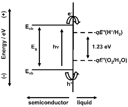
To use a single semiconductor and perform unassisted solar water splitting, the semiconductor needs to have a band gap energy (Eg) of >1.23 eV and the band edges of the conduction band and the valence band must straddle the electrochemical potentials E°(H+/H2) and E° (O2/H2O) as in Figure 1.1 to drive HER and OER.
However, the actual energy required is higher due to overpotential losses for electrochemical reactions, resistances losses from every part of the charge transfer process, and finally, the pH difference between the reductive and oxidative compartments. Due to the non-radiative recombination either in the bulk or at surface, the potential can be affected, resulting in a higher band gap, and the photocurrent can be affected as well partially because of the reduced utilization of the solar spectrum from the increased band gap. This will effectively degrade the solar-to-fuel conversion efficiency. Systems using single materials without external energy input can be achieved at a cost of low efficiency. Moreover, it also requires a proper band edge alignment to thethermodynamic potentials of the reduction and oxidation reactions. So far there is no single material that can do solar fuel conversion effectively and efficiently.
A tandem design which stacks two semiconductors together would be able to result in a better chemical conversion efficiency.[1] This enables the use of small band-gap materials including traditional photovoltaic semiconductors such as Si, group III-V, and group II-VI semiconductor families.
1.2 Fuel forming photocathodes
In the tandem design, a photocathode can be coupled with a counter anode or photoanode to form a PEC water splitting device. In this configuration, the cathode is photoactive. Photogenerated electrons are driven by the band bending in the p-type semiconductor to the interface between semiconductor and solution, reducing protons (low pH) or water (high pH) to hydrogen gas, while photogenerated holes are swept to the bulk and combine electrons flown from the anode[1].
Photocathode materials
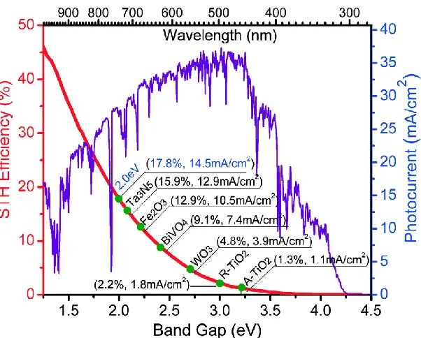
efficiently. Theoretical maximum solar to hydrogen (STH) efficiency versus bandgap is shown in Figure 1.3. 3) It should be stable during operational condition. This includes that the semiconductor is either intrinsically stable or protected. 4) The recombination of carriers should be low to reduce loss of the solar energy conversion efficiency. 5) The semiconductor is earth-abundant and inexpensive to reduce the cost of PEC and to compete with traditional fossil fuels.[5, 6]
Figure 1.3 Dependence of the theoretical maximum solar-to-hydrogen (STH) efficiency and the photocurrent density of photoelectrodes on the band gap under AM 1.5 G irradiation (100 mW cm−2)[6]. Reprinted with permission from Royal Society of Chemistry.
To date, there has been no material which satisfies all the requirements. Research is still ongoing to look for such materials. Materials that have been explored include metal oxides, Si, III-V group semiconductors, chalcogenides, and II-VI group semiconductors.
Silicon has a bandgap of 1.12 eV, which is a desirable small band gap to be used in dual band gap PEC systems[1]. Moreover, p-type Si has a suitable conduction band edge for HER. Si is also earth-abundant, making the cost competitive. As a widely used material in the photovoltaic industry, fabrication and processing methods of Si are mature. Research on Si photocathodes involves protection and band energetics engineering. Si is readily oxidized in aqueous solution, which needs a protective layer.
was stable for over 12h. Mathew et al.[8] reported an enhanced photoelectrochemical performance on Ru modified p-CdTe.
HER catalysts
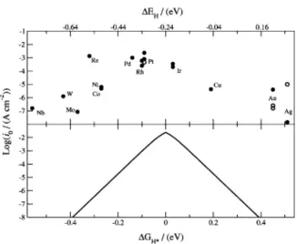
Small bandgap p-type semiconductors have been reported to have poor surface energetics for HER. To lower the activation energy and reduce overpotential, catalysts need to be incorporated onto photocathode surfaces to improve efficiency. Pt-group metals are known as the most efficient electrocatalysts for HER. Other Earth-abundant HER catalysts have also been explored.
Figure 1.4 (top) Experimentally measured exchange current, log(i0),log(i0), for hydrogen evolution over different metal surfaces plotted as a function of the calculated hydrogen chemisorption energy per atom (top axis). Single crystal data are indicated by open symbols. (bottom) The result of the simple kinetic model now plotted as a function of the free energy for hydrogen adsorption. [15] Reprinted with permission from ECS and the Copyright Clearance Center.
Pt is mainly used in acidic solutions because the reaction pathway is relatively simple and well elucidated[16]. It shows less great activity in alkaline solutions[17]. Yet Pt in base still shows more superior activity than most non-noble metal HER catalysts[18].
Photocathode protection/stability
prevent them from having reduction reactions. Even for p-Si photocathodes, surface oxidation is still an issue in idle conditions when the voltage is near open circuit potential, and a big issue when in alkaline solutions (Fig x.7 Si pourbaix diagram). What is worse is that even under cathodic protection, photocathodes are still readily oxidized. Research has shown that the dissolved O2 concentration has to be less than 15 ppb to prevent silicon oxidation during HER, which is not practical for a commercial water-splitting device[19]. The Chorkendorff group has developed several protective layers for p-Si photocathodes in acid. They first used a thin Ti layer to protect an n+p Si photocathode in 1.0 M HClO4 for 1h[20], then they developed a 100 nm thick sputtered TiO2 conductive protective layer on top of a thin Ti metal layer which protected an n+p Si photocathode in 1.0 M HClO4 during HER for 72 h[10]. Later on, they employed atomic layer deposition (ALD), which can deposit highly conformal and uniform coatings, to form a 100 nm TiO2 layer on 5 nm Ti/n+p Si photocathode. After being annealed in vacuum at 400 °C, this ALD TiO2 layer protected the photocathode for 2 weeks with less than 5% degradation during continuous HER in 1.0 M HClO4 for 30 days under constant illumination[21].
Other groups also used SrTiO3[22], TiO2[12, 23-25], and Al2O3[24, 26] to protect Si photocathodes in acid, with a stability from 35 h to 90 h. Protection of amorphous Si photocathodes have also been studied. With a TiO2 encapsulation layer, Javey et al.[27] demonstrated a 12 h stability for a-Si photocathodes with a 10% decay.
TiO2 can also be used to protect other p-type semiconductor photocathodes like p-InP. An amorphous TiO2 layer grown by ALD was able to protect p-InP nanopillars for more than 4 h with a stable HER photocurrent of 37 mA cm-2 in 1M HClO4[13].
1.3 Motivations
Photoelectrochemical (PEC) water splitting is a promising way to generate clean hydrogen fuel from water and sunlight. Due to the sluggish kinetics for HER on most semiconductor surfaces, catalysts are usually needed. The interface between the catalyst and the
semiconductor needs to be mechanically robust and able to conduct high electrical currents. A thorough understanding of the interface would be useful in designing HER
photocathodes. However, the understanding of the interfaces is very limited, and mostly confined to macroscopic scale. So we want to have a more detailed study of the mechanical and electrical properties of the interfaces, and it is good to be on a microscale or a
nanoscale. After understanding the interface, we would like to do some interfacial engineering as well.
Stability is also important for a good photocathode. Rigorous efforts have been made to stabilize photoanodes, with less focus made on the photocathodes part. CdTe is predicted to be stable thermodynamically in the pourbaix diagram from calculation, and has been used in photovoltaic devices. It would be interesting to study how stable it is under PEC operation conditions.
1.4 Contents of the thesis
In Chapter 2, the interfacial properties of electrolessly deposited Pt nanoparticles (Pt-NPs) on p-Si and p+-Si electrodes were investigated on the nanometer scale using a combination of scanning probe methods.
In Chapter 3, the interface between p-Si and Pt was engineered with TiO2 by atomic layer deposition (ALD). The annealed TiO2 showed a higher open circuit voltage Voc than the as grown one. It was further investigated in aqueous and non-aqueous redox couple solutions and XPS to understand how the interfacial layer changed during annealing.
In Chapter 4, the stability/corrosion of dark CdTe electrodes were studied in 1M H2SO4 and 1M KOH, at -100 mV vs. RHE bias and at open circuit voltage. Chemical corrosion and electrochemical corrosion were compared, and corrosion of dark CdTe electrodes with Pt catalyst was also studied.
C h a p t e r 2
NANOSCALE ELECTRICAL AND MECHANICAL
CHARACTERIZATION OF THE PT/SI INTERFACE
Content in this chapter is drawn from the following publication:
Jiang, J., Huang, Z., Xiang, C., Poddar, R., Lewerenz, H.-J., Papadantonakis, K. M., Lewis, N. S., Brunschwig, B. S. Nanoelectrical and Nanoelectrochemical Imaging of Pt/p-Si and Pt/p+-Si Electrodes. ChemSusChem10, 4657 – 4663 (2017). DOI:
10.1002/cssc.201700893.
Jiang, J. participated in the conception of the project, imaged samples in the air and analyzed the data, assisted in the AFM-SECM experiments in the electrolyte, and participated in the writing and revision of the manuscript.
Photoelectrochemical (PEC) water-splitting systems place catalysts for the water-splitting half-reactions in electrical contact with semiconducting photoelectrodes that convert light energy into separated positive and negative charges. [2] [3] [4] In such systems, the interfaces between the light absorbers and catalysts must provide a robust mechanical attachment of the catalyst to the surface as well as a pathway for charge to flow from the light absorber to the catalyst.
Electroless plating is a widely used method for the deposition of metal catalysts onto photoelectrodes.[31-34] Kulkarni and coworkers have summarized the history of electroless deposition methods, including optimization of plating conditions (concentration, pH, temperature, etc.), particle density on the surface, and proposed particle-growth mechanisms.[35]
between the electrolessly deposited particles and the Si substrate, whereas no interfacial Si oxide is observed for evaporated Pt.[34] Further, weak adhesion has been observed for some metals films and nanoparticles (NPs) to Si surfaces with SiO2 layers.[36-39]
The present understanding of interfaces between Pt NPs and Si substrates is derived primarily from macroscopic measurements, as opposed to methods that provide information about the electrical and electrochemical properties of individual NPs.[40],[41]
We describe herein the electrical and mechanical properties of individual electrolessly deposited Pt NPs on Si(111) surfaces as measured using atomic-force microscopy (AFM). The electrical and mechanical properties were measured both in air and in contact with an electrolyte. The surface topography and conductivity of electrolessly deposited Pt NPs were simultaneously imaged by AFM. The force needed to move the particles on the surface was measured, and the area under the particles examined. Furthermore, the conductance of the particles in contact with an electrolyte was mapped using AFM-based scanning electrochemical microscopy (SECM).
2.1 Pt/Si sample fabrication
Materials
Boron-doped, Czochralski-grown Si wafers with resistivities, ρ, of∼ 7.5 (p-Si) and < 0.005 Ω·cm (p+-Si) were purchased from Silicon Resource Inc. All other chemicals used were obtained commercially (see Supporting Information). H2O with a resistivity of 18 MΩ∙cm was obtained from a Barnstead Nanopure station (Thermo Scientific).
Fabrication of electrodes for microscopic studies
with N2(g) and immediately submerged in a Pt electroless plating solution for 45 s, followed by a thorough rinse with H2O. The Pt electroless plating solution consisted of 1 mM H2PtCl6(aq) in 0.50 M HF(aq). A diamond scribe was used to scratch a Ga/In eutectic mixture (Aldrich) onto the back side of each Pt/Si chip.
Characterization of deposited Pt nanoparticles
Conductive AFM using PeakForce tapping (PFT) mode on a Bruker Dimension Icon atomic force microscope (AFM) was used to characterize the morphology, interfacial mechanics, conductivity and electrical properties of the electrode surfaces.[42] Conductivity imaging while mapping the surface topography was done using PeakForce Tunneling AFM (PF-TUNA).
AFM-SECM was done on the same Dimension Icon AFM using a PF-SECM with commercial probes obtained from Bruker. In PF-SECM, alternating line scans are run in PFT and lift modes. In lift mode, the tip does not oscillate and follows the topographical profile obtained by the previous PFT scan at a defined height above the surface. In this work, the lift height was 100 nm. The topography and conductivity of the sample were captured in PFT mode, and the electrochemical current was measured in lift mode. The currents during contact between the tip and the surface in the presence of an electrolyte were measured using a different algorithm than the contact currents measured in air by PF-TUNA.
For the electrochemical studies, an aqueous solution of 10 mM [Ru(NH3)6]]3+ and 0.1 M KCl was used. A CHI760 bipotentiostat (CH Instruments, Texas) was used to control the electrochemical conditions. The electrochemical cell had a Pt wire counter electrode and a AgCl-coated Ag wire as a quasi-reference electrode (AgQRE). In the SECM scan the tip was biased at -0.4 V vs AgQRE to reduce the [Ru(NH3)6]3+, while the sample was held at -0.1 V vs AgQRE to reoxidize any [Ru(NH3)6]2+ generated by the AFM tip.
(30%): conc. HCl(aq) (37%) and was maintained at 75 oC. The solution for electroless deposition of Pt consisted of 1 mM H2PtCl6(aq) in 0.50 M HF(aq). A diamond scribe was used to scratch a Ga/In eutectic mixture (Aldrich) onto the back side of each Pt/p-Si chip. For AFM studies, 1.0 x 1.0 cm chip samples were mounted onto an SPM sample-mounting disk (SD-101, Bruker) using Ag paint (SPI, Inc.), and allowed to dry overnight. For PF-SECM measurements, a 3.8 x 3.8 cm p+-Si chip was loaded onto a flat Cu foil of the same size, instead of a sample-mounting disk.
2.2 Nanoscale characterization of deposited Pt/Si
Peak Force tapping mode (PFT): In PFT mode, the probe was sinusoidally modulated at a low, off-resonance frequency. The frequency was 1 or 2 kHz with an amplitude of 100 or 150 nm. The feedback signal in PFT was the maximum force between the tip and the sample during every tapping cycle. The tip intermittently contacted the surface for ~ 100 to 300 µs. For surface topography mapping, ScanAsyst-air probes (Bruker) with a nominal tip radius of 2 nm were used. The surface was scanned using a relatively rapid line scan (left to right) while slowly moving the tip in the orthogonal direction (vertical in the plotted figures). Generally only data from the reverse scan direction (right to left, retrace) was used.
Peak-Force Tunneling AFM (PF-TUNA) mode: To capture current signals under an applied sample bias, an electronic module with a bandwidth of 10–20 kHz was used.[43] The PF-TUNA software algorithm allowed capture of currents during the period of maximum contact force, averaged over the contact duration (contact current), and averaged over the whole tapping cycle (TUNA current). The conductive probes used were SCM-PIT probes from Bruker with Pt/Ir coating layers and nominal tip radii of 20 nm. The imaging force was 5 – 10 nN.
from left to right. When the script was complete, the same area of the surface was re-imaged using conventional tapping mode.
Peak-Force Scanning Electrochemical Microscopy (PF-SECM): PF-SECM was used for local, in situ electrical and electrochemical measurements using commercially available nanoelectrode probes from Bruker. The probes were fully coated by SiO2 except for the Pt conical tip apex with a height of ~200 nm and an end tip diameter of ~50 nm. The detailed electrochemical characterization of these probes has been reported previously.[44, 45] Electrochemical studies by PF-SECM were performed using an aqueous electrolyte solution of 10 mM [Ru(NH3)6]]3+ and 0.1 M KCl. The electrochemical cell had a Pt wire counter electrode and a AgCl-coated Ag wire as a quasi-reference electrode (AgQRE). A CHI760 bipotentiostat (CH Instrument, Texas) was used to control the electrochemical conditions. The probes were briefly tested by running a few cyclic voltammograms at a scan rate of 50 mV/s in the AFM electrochemical cell (Bruker). The surface area of the nanoelectrode probe was ~10-9 cm2. [44, 45] A typical particle in the SECM image (Figure 2.7) had an apparent size of ~ 140 x 180 nm. If the particle is treated as a sphere of 160 nm, the surface area is ~10-9 cm2. Thus when the AFM-SECM tip was in contact with a particle on the surface, the active area for [Ru(NH3)6]]3+was approximately doubled.
tip. Approaching the tip to a highly resistive region on the surface where [Ru(NH3)6]2+ is not reoxidized led to a reduction in tip current (negative feedback). For a conductive region where [Ru(NH3)6]3+ was regenerated, a positive feedback was observed.[2a] These distinct responses allowed imaging the inhomogeneity of the conductance on the sample surface. Before SECM mapping, the approach curve (tip current vs tip-sample distance) of the nanoelectrode probe was measured on a particle-free region of the surface. The tip was biased at -0.4 V vs AgQRE.
2.3 Resistance Measurements
p-Si resistance:
7.5 0.052 0.375 1
l cm
R cm
A cm
Pt particle (50 x 50 x 50 nm) resistance:
9 7 9 9 50 10
1.1 10 2.2
50 10 50 10
l m
R m
A nm nm
Pt/Ir tip resistance: ~10Ω from vendor
2.4 Results
2.4.1 Topography and Conductivity of Pt/p-Si in air
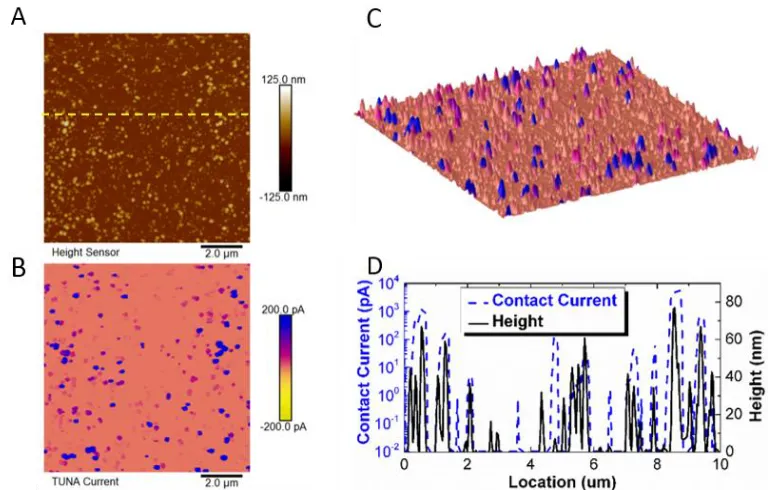
The current-voltage (I-V) data measured for individual particles showed rectifying behavior; however, the I-V behavior under forward bias varied substantially from particle to particle. For particle #1, #2 and #3, the currents started rising at ~0, ~0.1 and ~0.3 V, respectively. No nanoparticle was present at location #4, and negligible current (1.8 to -1.4 pA) was measured at this location.
Figure 2.1. Topography, conductivity, and current-voltage (I-V) spectroscopy of Pt nanoparticles electrolessly deposited onto a p-Si substrate and measured in air. (A) Surface topography. (B) and (C) contact currents shown for sample biases of 0.3 V and -0.3 V, respectively. (D) Cross-sectional analysis of surface topography (green-dashed), contact current at 0.3 V (blue-solid) and -0.3 V (red-dotted) sample biases for the portion of the sample indicated by the yellow-dashed line in (A), (B) and (C). The left and right ordinates are contact current and surface topography, respectively. (E) Point-specific I-V
Figure 2.2 PF-TUNA scan of the same region of the Pt-NP/p-Si surface at 0.3 V shown in Figure 2.1. (top) Contour plot of the surface topography after flattening; (bottom) Logarithm of the absolute value of the current. Note that the larger particles showed contact currents, and notice that the observed currents varied by a factor > 1000. Replotted from Figure 2.1AB to more clearly show the variance in scale.
The I-V data of particles #1 – 3 were fitted to the thermionic emission equation (Equation 2.1) considering a series resistance in the circuit:
( ) 2
( ) * 1
B
B B
q q V IR
k T nk T
I V AA T e e
(2.1)
absolute temperature, q is the unsigned charge of an electron, kB is Boltzmann’s constant;
φB is the barrier height, n is the ideality factor, and R is the resistance of the sample. Fitted results are plotted as solid lines in Figure 2.1E, and the fitted values of φB,n, and R are listed in Table 2.1. The particles had barrier heights of ~ 0.55 V with resistances of 12 – 60 MΩ.
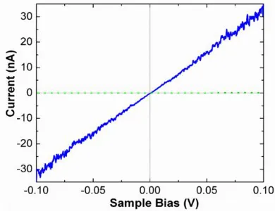
Figure 2.3 Expanded plot for Figure 2.1E. I-V data (blue solid line) captured from the Pt-TF/p-Si sample. The resistance obtained from the data was 3 106 Ω.
[image:35.612.226.421.183.333.2]Table 2.1. Results from fitting the I-V data for particles #1–3 to the thermionic emission equation with a series resistor (Equation 2.1). Parameters are described in the text. The I-V
data of the Pt thin film / p-Si was fitted to Ohm’s law.
Particle φB (eV) n R (MΩ)
1 0.53 1.5 49
2 0.52 2.6 12
3 0.57 1.4 63
Thin film
N/A N/A 3
Figure 2.4. Topography and TUNA current for Pt nanoparticles electrolessly deposited onto a p- Si substrate captured by PF-TUNA. (A) Surface topography; (B) TUNA current at a sample bias of 0.5 V; (C) The 3-D rendering of the surface topography painted by the false-color current map; and, (D) Cross-sectional analysis of the surface topography (solid grey) and TUNA current (dashed blue) at the same sample location as indicated by the yellow dashed line in (A). As shown in Figure 2.1, the contact currents varied from the detection limit of <1 pA to 103 pA (Figure 2.2). Figures 2.2 and 2.4 both show this same amount of variation. The line profile plot in Figure 2.1D only shows currents < 40 pA, because the line was not drawn through any high current points, as shown in Figure 2.1B.
2.4.2 Topography and Conductivity of Pt/ p+-Si in air
~10 pA (for a particle not evident in the topographic image) to ~50 nA (a factor of 103 larger than for Pt-NP/p-Si). Figure 2.5C shows I-V data for the locations labeled in Figure 2.5A. Particles #1 and #2 showed relatively ohmic behavior in this measurement window, with resistances of 1.5 and 26 MΩ, respectively, between -50 and 50 mV. A Pt-TF/p+-Si sample showed location-independent ohmic I-V data with a resistance of 2 kΩ.
[image:38.612.109.352.204.311.2]2.4.3 Adhesion for Pt-NP/p+-Si in air
A TESPA probe was used to evaluate the adhesion of the particles to the substrate. The probe had a nominal spring constant of 40 N/m, ~20 times that of the SECM probe (2.2 N/m) used below. During the pushing process, a particle was first locally detected using conventional tapping mode. The tip oscillation was stopped and then the tip was held 10 nm above the surface while moving from left to right across a particle for more than 1 µm. Particles subjected to pushing had heights of > 150 nm.
Figures 2.6A-B present the surface topography for an area of the sample before and after the particle-pushing process for samples in contact with air.
Figure 2.6 (A) Surface topography for a sample area imaged by classic tapping mode in air before the pushing process. Yellow arrows and numerical labels indicate the four particles subjected to pushing from left to right by the probe tip. (B) Surface topography of the same area in (A) imaged by classic tapping mode in air after the pushing process; and (C) line profiles for the four particles indicated in (A). From left to right are particle #1 (red line), #2 (blue line), #3 (pink line), and #4 (green line). (D)-(E) Zoomed-in views of particle #2 before (D) and after (E) pushing.
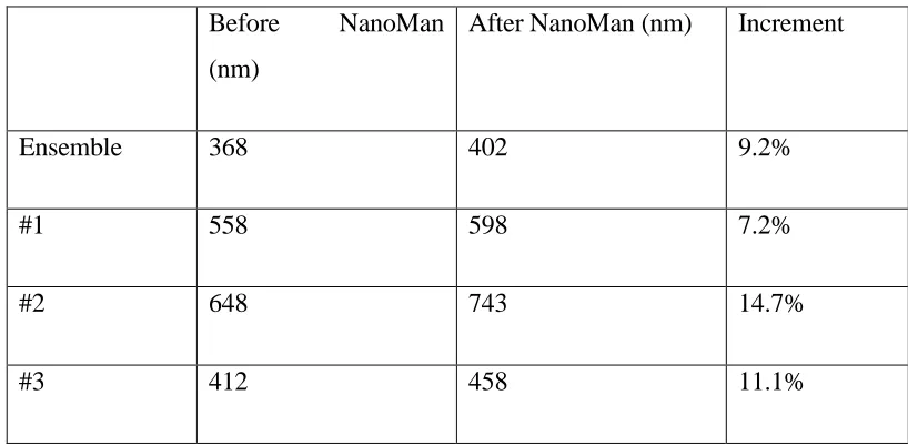
cantilever during the pushing attempt resulted in bending the cantilever > 100 nm, corresponding to a force of > 4 µN. This contact force would be expected to dull the tip. An ~10% increase in the mean apparent particle diameter was observed after pushing, consistent with dulling of the probe tip (Table 2.2).
Table 2.2. Apparent mean diameters of the particles in Figure 2.6A and 2.6B before and after Nanoman pushing.
Before NanoMan (nm)
After NanoMan (nm) Increment
Ensemble 368 402 9.2%
#1 558 598 7.2%
#2 648 743 14.7%
#3 412 458 11.1%
2.4.4 Adhesion for Pt-NP/p+-Si in electrolyte
originally, inferred from the size and distribution of the holes, and the particles were pushed to the edges of the surface. The depressions had depths between 0.2 and 0.8 nm and showed a variety of in-hole structures. Figure 2.8 shows the cross-sectional analysis of a typical hole, which exhibited a width and depth of ~150 and ~ 0.7 nm, respectively.
Figure 2.8 Indentations remaining on the Si surface after the particles were moved away by the SECM probe in 0.1 M KCl(aq). The on-image plot is a cross-sectional analysis of the line profile across a hole as indicated by the yellow dashed line.
2.4.5 SECM of Pt-NP/p+-Si in electrolyte
Figure 2.10 PeakForce SECM imaging of Pt nanoparticles electrolessly deposited onto a degenerately doped p+- Si substrate and in contact with 10 mM [Ru(NH3)6]3+ and 0.1 M KCl(aq) with an imaging force of 700 pN and a tip velocity of 1.2 µm/s. The nanoelectrode probe and the sample were biased at -0.4 V and -0.1 V vs a AgCl-coated Ag wire as a quasi-reference electrode (AgQRE), respectively. A 3 µm x 750 nm area was scanned. (A) Surface topography. (B) Tip-contact current captured during the main PeakForce-tapping scan. (C) Electrochemical current captured during the lift scan at a lift height of 150 nm. The scale bar is 600 nm.
To confirm that the measured current originated from the tip apex rather than the sides of the tip, the approach curve of the nanoelectrode probe was measured over a particle-free region of the Pt/p+-Si electrode (Figure 2.9B) while the tip was biased at -0.4 V vs AgQRE to obtain a diffusion-limited current. The tip current decreased from 1.38 nA at a tip-sample distance of 1 µm to 1.05 nA when the tip was at the sample surface. The 25% reduction in current is consistent with simulations reported in previous work.[47]
[image:45.612.161.478.85.295.2]Figure 2.12 Same PeakForce SECM scans shown in Figure 2.10 for Pt nanoparticles electrolessly deposited onto a degenerately doped p+- Si substrate and measured in contact with 10 mM [Ru(NH3)6]3+ in 0.1 M KCl(aq). (top) Contour plot of the topography of surface; (middle) Contour plot of the common logarithm of the tip contact current; (bottom) Contour plot of the common logarithm of the SECM current.
[image:48.612.134.466.131.495.2]by a comparison of Figures 2.2 and 2.4 with Figure 2.11. This behavior was in part due to the Faradaic current observed even when the tip was in contact with an electrochemically inactive area of the surface. The SECM current near the center of the image was ~1.40 nA. For particles in region #4, the SECM current increased by ~ 50 pA, while the current increased by ~0.18, 0.14 and 0.17 nA for particles #1, #2 and #3, respectively. The electrochemical imaging resolved the particles in region #4. These correlated maps allowed comparison between the surface topography, contact current and SECM faradaic current for the different particles. For example, particle #2 and #3 both had sizes of ~120 x 200 nm and a height of ~65 nm, but particle #2 had a tip-contact current ~ 5 times larger than that of #3 while exhibiting an SECM current ~20% less than particle #3.
KCl (aq) at a scan rate of 50 mV/s. A Pt wire was used as the counter electrode and a Ag wire coated with AgCl was used as the quasi-reference (AgQRE) electrode. (B) Approach curve (tip current vs tip-sample distance) captured under the same electrochemical conditions through force ramping the SECM probe at a triggered force of 10 nN and a ramp rate of 0.25 Hz. The normalized current is shown on the right ordinate axis.
2.5 Discussion
PtCl62- and PtCl42- are strong oxidants (E0 ~ 0.7 V vs NHE for the PtCl62-/PtCl42- and PtCl4 2-/Pt couples). Thermodynamically, these metal cations can oxidize Si, and in the presence of water, SiO2 can form on the surface, eq 2.2.
H2PtCl6 + Si0 + 2 H2O Pt0 + SiO2 + 6 HCl (2.2)
SiO2 + 6 HF H2SiF6 + 2 H2O (2.3)
The electron affinity of bulk Si(111) has been estimated to be 4.05 eV[48] and the Si band gap is 1.12 eV. Thus, under flat-band conditions, the valance-band edge of Si is located at a potential of 5.17 V vs vacuum.[48] Pt has a work function of ~5.6 eV[49], so the band positions suggest that an ideal Pt/Si contact would be ohmic, as is generally observed for p-Si.[46] The rectifying behavior observed on the nanoparticle samples can thus be attributed to the interfacial Pt-NP/Si junction, which produces a resistive diode-like junction. Although a resistive junction is not desired for kinetic reasons (current), the observed high barrier height due to the rectifying junction benefits the energetics (photovoltage).
The Pt-NP/p+-Si samples yielded ohmic behaviors, as expected for two metallic materials in contact, even if a thin oxide layer exists at the interface. The Pt-NP/p+-Si junction was more conductive locally than the Pt-NP/p-Si junction (1.4-26 vs 10-60 MΩ), similar to observations for the Pt-TF/p-Si. The high resistances observed for the particles may be due in part to the SiO2 layer between the silicon and the Pt-NPs.
The mechanical adhesion is not robust between a Pt thin film and Si. An interfacial adhesion layer is consequently normally required when Pt is deposited by physical vapor deposition onto Si substrates. For a Pt thin film deposited directly on Si, imaging forces of < 10 nN did not damage the surface in air. The Pt-NP/Si sample showed strong mechanical attachment of the particles to the substrate in air, and even a stiff cantilever did not push the particles away from the surface. However, the adhesion changed substantially in aqueous solution, and under such conditions intermittent contact imaging with a force < 1/20 of that used in air pushed the Pt nanoparticles out of the imaging scan. The presence of an electrolyte may change the interfacial energetics at the semiconductor/metal junctions,[50-52] and such changes may be due to the change of interfacial mechanics.
Although only loosely attached to the Si surface when in contact with an electrolyte, currents were passed by the particles, with some particles supporting high current densities. For example, the tip-contact current depicted in the SECM scans of Figures 5B and S7 was > 7 nA for particle #2. The tip was in contact with the particle for only a small part of the tapping cycle, so the contact current was actually ~ 6 times larger than the measured current, or > 40 nA (see PF-SECM in experimental). For a particle of ~3 104 nm2, this value corresponds a current density of ~ 102 A cm-2.
The tip-contact current observed during the SECM scan results from two sources: 1) current due to the potential difference between the tip and the substrate, and 2) current due to the reduction of Ru(NH3)63+ in solution. The SECM tip is a Pt-coated cone ~250 nm in height, and therefore remains exposed to the solution even when in contact with the surface.[55] For samples in contact with an electrolyte, the reduction current measured during tip contact can thus increase relative to the current measured during lift mode. Substantial tip-contact current can thus be present even in areas that do not contain particles.
The SECM current varied from 1.37 to 1.6 nA at 100 nm above the surface, whereas the diffusion-limited current at 1.0 μm above the surface was ~ 1.4 nA, Figure 2.9. The SECM currents measured above the Pt-NP/p+-Si surface were <1.6 nA, with the SECM current surface showing small peaks on a convoluted surface, Figure 2.11-S7.
The observed tip-contact current showed a minimum value of about 1.3 nA, slightly less than the minimum SECM current. The approach curve data, Figure 2.9B, suggest that the tip-contact current for a particle-free region would show ~ 10% lower currents than the SECM current obtained 100 nm above the surface. A tip-contact current of ~1.3 nA is thus expected even in a particle-free region, in accord with observations. Moreover, all of the NPs observed in the topological scan should show a tip-contact current > 1.3 nA due to the enlarged effective tip area, again in accord with observations.
reductive current due to diffusion in the solution. This observation agrees with the PFT scans in air, which indicated that only about half of the particles showed a contact current. The SECM current surface had a convoluted shape that closely matched that of the tip-contact current surface (if one ignores the three large peaks, Figure 2.11). The similarity of the SECM and tip-contact current surfaces is expected if the source of both currents is primarily due to reduction of Ru(NH3)63. The tip-contact current for some of the particles was ~7 nA, e.g., particle #2 in Figure 2.10B, which is a much larger current than that displayed by most of the other particles. In such cases, current flowing through the Si via the Pt NP to the tip contributes substantially to the total current. If the actual contact current for particle #2 is ~40 nA, as estimated above, then the resistance for current flow through the particle is ~ 10 MΩ, consistent with the measurements made in air.
The variation in contact and SECM currents, as well as the differences in the depressions under the particles, suggest that the electrochemical performance of electrolessly deposited Pt particles is not only the result of the uniformly low activity of all the particles, but also arises from the wide range of conductance through the particles that allows only some of the NPs to contribute substantially to the bulk electrochemical activity of the surface.
2.6 Conclusion
The electroless deposition resulted in particles that were slightly embedded into the Si. The particles were mechanically well attached to the sample surface in air, whereas in contact with an aqueous electrolyte the adhesion of the particles to the surface was substantially weaker, and surface imaging required the use of sub-nN force.
C h a p t e r 3
UNDERSTANDING THE IMPROVEMENT OF
PHOTOELECTROCHEMICAL WATER SPLITTING ON P-SI WITH
ANNEALED ATOMIC LAYER DEPOSITED TIO
2Content in this chapter is drawn from the following publication:
Jiang, J., Liu, R., Mayer, T., Mitrovic, S., Richter, M., Zhou, X., Sun, K., Papadantonakis, K. M., Brunschwig, B. S., Lewis, N. S. Understanding the Improvement of
Photoelectrochemical Water Splitting on p-Si with Annealed Atomic Layer Deposited TiO2. (In preparation)
Jiang, J. participated in the conception of the project, prepared samples, conducted electrochemical measurements, analyzed data, and participated in the writing and revision of the manuscript.
Many small band gap semiconductor photocathodes that are potentially useful for water splitting are unstable towards decomposition or surface reactions under illumination in aqueous electrolytes.[56] Relatively thick films of TiO2 have recently been used successfully as a protective layer for photocathodes, which functions as an electron conductor by charge carrier movement in the TiO2 conduction band.[57-62] The interfacial energetics between the semiconductor and the electrolyte, and the ability to tune the energy of the photogenerated electrons that couple to the electrocatalysts on top of the TiO2 film, have not been well elucidated. Understanding and controlling energetics of these heterojunctions are crucial to the utilization of this approach for protection of small band gap semiconductors such as Si, GaAs, and GaP for the solar-driven water splitting.[63] Thus, detailed studies of the interfacial energetics of semiconductor interfaces with TiO2 will be performed as the key focus of this field.
TiO2 conduction band. Therefore the energy of the photogenerated electrons that is transferred to the catalyst should be dictated by the energy of the TiO2 conduction band edge. Therefore, the simplistic picture of electrons having the potential on the TiO2 conduction band edge clearly does not apply to this situation since the difference between the water reduction potential (VHER) to TiO2 conduction band edge are too close to support high efficient water reduction current. Additionally the value of the photovoltage should be affected both by the photocathode/TiO2 interface and the redox potential of the electrolyte plus the water reduction catalyst.
In this study, we deposit TiO2 onto the surface of silicon by employing the atomic layer deposition (ALD). As an earth abundant material, silicon stands out as one of the most promising semiconductors, with its outstanding good performance on light absorption, incident photon to electron conversion efficiency, charge transfer property, etc. for solar energy driven devices. As a photocathode, the electrons generated by solar irradiation in silicon easily flow from its conduction band into the TiO2 passivation layer, and are then injected into the electrolyte for reduction reactions. By using ALD, the condition of TiO2 layer on Si surface can be carefully controlled. Investigating the passivation layer thickness effect, the annealing effect, and the redox potentials influences in this paper can help to understand the energetic structure of Si/metal oxide heterostructures and the origins of improving water splitting efficiency.
3.1 Experimental
Substrate preparation
Atomic-layer deposition of TiO2
TiO2 deposition was performed using a Savannah ALD system (Cambridge Nanotech). The substrates were heated to 150 °C in a chamber held at a constant pressure of 0.2–0.3 Torr. The precursor, TDMAT (Tetrakis(dimethylamino)titanium, Sigma Aldrich, 99.9999% pure), was heated to 75 °C and was swept into the ALD chamber for 0.1 s using consecutive pulses of N2 at a flow rate of 20 sccm. The remaining TDMAT was purged from the system for 15 s using nitrogen gas, and then water was pulsed for 0.015 s. Upon completion of ALD, the samples were removed from the chamber and stored under ambient conditions until analyzed. Half of the samples were annealed in air at 400 °C for 1 h in a Thermolyne furnace (Thermo Scientific), and the other half were left as grown.
Deposition of Pt films
2~3 nm of Pt (Kurt J. Lesker, 99.99%) was deposited onto the TiO2 covered Si substrate in a sputter system (AJA International) with a base pressure of < 10−6 torr. Control samples were made to compare stability to the TiO2/Pt samples by depositing Pt nanoparticles electrolessly onto p-Si electrodes using 1.0 mM H2PtCl6 in 0.5 M HF (aq) for 2 min, followed by a thorough rinse with H2O and dried by N2.
Photoelectrochemistry
The electrodes were fabricated by cutting samples into ~ 0.10 cm2 pieces, scratching Ga/In eutectic mixture (Aldrich) on the back, and using Ag paint (SPI, Inc.) to mount samples on coiled Cu wires (Consolidated Electronic Wire & Cable). The wire was threaded through a glass tube, and the edges of each sample were covered by Hysol 9460 epoxy to define the active electrode area. Electrode areas were determined by imaging the electrodes on an optical scanner (Epson Perfection V370) and calculated in ImageJ software.
continuously bubbled by H2 (research grade, AirLiquide) to maintain a constant RHE potential. A saturated calomel electrode (SCE) (0.244 vs. NHE (normal hydrogen electrode), CH Instruments) and a carbon cloth electrode in a fritted glass tube (Porosity D, Ace glass) were used as the reference and counter electrodes, respectively. The electrochemical behavior was measured using cyclic voltammetry (CV) at a scan rate of 50 mV s−1 either in the dark or under simulated 1 Sun illumination provided by an ELH lamp. Stability is measured using 100 cycles CV with scan voltage range from open circuit voltage to the voltage where light limit current has been reached.
The measurements in methyl viologen were carried out under continuous purging of Ar. The electrolyte consisted of 0.5 M K2SO4 and 50 mM methyl viologen dichloride (MV2Cl2, 98%, Sigma-Aldrich), and was buffered at pH = 2.9 using 0.1 M potassium hydrogen phthalate and sulfuric acid. Prior to measurements, after excluding oxygen by purging Ar for 1 hour, MV+ radical was generated in situ, by scanning CV between -0.6 V and – 0.9 V versus Ag/AgCl reference electrode, until the solution potential reached -0.6 V versus Ag/AgCl, with a carbon rod electrode as a working electrode, and a carbon cloth electrode in a fritted glass tube (Porosity D, Ace glass) as a counter electrode, and a Ag/AgCl (1M KCl, 0.235V vs. NHE, CH Instruments) as a reference electrode. The generated MV+ radical cation was ~ 3 mM, and made the electrolyte turn deep blue. Photoelectrochemical data was collected at an incident 850 nm light intensity (band width 30 nm) of 60 mW cm -2, with the sample electrode as a working electrode, a carbon rod electrode as a counter electrode, and a small carbon cloth electrode as a reference electrode. The open circuit voltages of the samples were measured using Open Circuit Voltage (OCV) technique for 30 s.
contains 2 mM cobaltocene (CoCp2, 98%, ACROS Organics), and 80 mM cobaltocenium hexafluorophosphate (CoCp2PF6, 98%, Sigma-Aldrich. For tests in decamethylferrocenium/decamethylferrocene, the electrolyte contains 5 mM decamethylferrocene (Me10Fc, 99%, Alfa Aesar), and 25 mM decamethylferrocenium tetrafluoroborate (Me10FcBF4). For tests in ferrocenium/ferrocene, the electrolyte contains 5 mM ferrocene (Fc, 98%, Sigma-Aldrich), and 25 mM ferrocenium tetrafluoroborate (FcBF4, technical grade, Sigma-Aldrich). Acetonitrile was dried by flowing through a solvent column, and stored in 3Å, activated, molecular sieves (Sigma-Aldrich). LiClO4 was dried by fusing under a pressure < 1×10⁻³ Torr at 300 °C. Other chemicals were purified by vacuum sublimation. The chemicals were all stored in glove box that contained less than 0.2 ppm of oxygen. The electrochemical measurements were carried out in glove box as well. The open circuit voltages of the samples were measured using Open Circuit Voltage (OCV) technique, under simulated 1 Sun illumination provided by an ELH lamp, with the sample electrode as a working electrode, a Pt gauze (52 mesh, 0.1 mm diam., 99.9%, Alfa Aesar) as a counter electrode, and a Pt wire (0.5 mm diam., 99.99%, Sigma-Aldrich) as a reference electrode.
Mott-Schottky analysis
XPS Characterization
XPS characterization was performed on a Kratos AXIS Nova with DLD (Kratos
Analytical, Manchester, UK, a Shimadzu Group Company). We used a monochromatic Al K line at 1486.6 eV from a source operating at 15 mA and 15 kV. Spectra were acquired at the pressure at low 10 -9 Torr, with a spot size of 700 m by 400 m, pass energy 10 and a step of 50 meV. Sample surfaces were cleaned only by a nitrogen blow-off, and then contacted from the top. We did not apply charge neutralization.
3.2 Results and discussion
TiO2 protection layer showed relative stable Voc. Considering some potential drop on ALD TiO2 protection layer, the Voc was irrelative to the thickness of TiO2. It implied that the as-grown ALD TiO2 protection layer would not contribute too much on the band bending on the energy structure.
Figure 3.1. J-V characterization of the Si/TiO2/Pt heterojunctions in 1.0 M H2SO4 aqueous solution. The J-V curves of 20, 40, 80, 250, 500 cycles of ALD TiO2 on Si/TiO2/Pt heterojunctions were shown (a)-(e). Zoomed in figures on the onset potential region of (a)-(e) were exhibited in (f)-(j) respectively. Red solid line: Annealed TiO2 on p Si with sputtered Pt. Blue solid line: As grown TiO2 on p Si with sputtered Pt. Gray dash line: Pt disk electrode.
[image:60.612.162.528.215.453.2]comparable to the record of 520 mV obtained on the similar structure of p-n+ Si/TiO2/Pt. Large Voc of 440 and 456 mV were also observed on p-Si with 20 cycles and 80 cycles of ALD TiO2. However, this effect seemed diminished on the thicker TiO2 samples. Voc of 250 cycles (10 nm) ALD TiO2 sample will decrease to 280 mV, while the 500 cycles (20 nm) one has only 60 mV difference with the as-grown TiO2 samples (182 mV vs. 122 mV). The ALD TiO2 surface does not change the roughness, which was approved by AFM (Figure 3.2). Thus it excluded the possibility of annealed ALD TiO2 forming micro-size grains during annealing, exposing p-Si into the solution, and therefore may result in a higher Voc.
Figure 3.2 AFM images for the Si/TiO2 heterojunctions before (a) and after (b) annealing
the newly formed Si-O-Ti layer had good electron conductivity for water reduction. The abridged anodic currents of these annealed thin TiO2 samples indicated that the hole conductivity of these Si-O-Ti layers may not be good enough to complete water oxidation. This was consistent with the results of the previous report.[63, 66]
Moreover, this Si-O-Ti was different from the other non-controlled SiOx layer on the electronic property. By heating bare p-Si without ALD TiO2 in air under same annealing condition, a SiOx layer was intentionally fabricated onto p-Si. With the same amount of Pt sputtered onto this p-Si/SiOx, the sample was not photoreactive until over -1.0 V (vs. SCE) bias was applied in 1.0 M H2SO4 solution. If we calculate the water splitting efficiency by the following equation,
(3.1)
Figure 3.4. Efficiency of the Si/TiO2/Pt heterostructures.
Figure 3.5. Mott-Schottky plots for (a) as grown and (b) annealed p Si/250 cycles TiO2.
To study the interface energetics, we performed solid-state Mott-Schottky analysis on p Si/TiO2 samples with 250 cycles TiO2, as grown and annealed:
(3.2)
where ND is the doping density, ε is the relative dielectric constant of semiconductor, ε0 is the permittivity of the vacuum, e is the charge of an electron, A is the electrode surface,
k is the Boltzmann constant, T is the temperature, and Vfb is the flat band potential at
the semiconductor/electrolyte interface. The intercepts of the linear extrapolation in the Mott-Schottky plots indicate flat band potential Vfb, which were 0.21 V and 0.40 V for the as grown samples and annealed ones, respectively. The Vfb of the annealed samples showed a significant positive shift, which implied greater band bending on the annealed samples and was in agreement with the improvement of Voc.
a carbon rod counter electrode. The Voc obtained (Figure 3.5a) on varied thickness of as grown ALD TiO2 show similar trend of the corresponding ones in 1.0 M H2SO4 (Figure 3.4). The only difference was that the 20 cycles of as grown TiO2 on p-Si had higher Voc than the corresponding one in 1.0 M H2SO4. It was because in such a reactive solution, oxidation of the Si rarely happened since MV•+ was reactive and much easier to be oxidized,[67] and the TiO2 layer was too thin to influence the depletion region of Si and the chemical potential of the solution. With increased thickness of TiO2, the additional energy level was formed, which made electrons an intermedia energy station with lower energy level and therefore lowered the Voc. After annealing, all the samples had enhanced
Voc, indicating that the assumption of the new formed buried junction between p-Si and
Si-O-Ti mixture. The maximum Voc obtained was 517 mV on 40 cycles of annealed ALD TiO2, which was close to the result of 510 mV on homogenous junction p-n+ Si/TiO2 in fast redox pair solution. It meant that the quality of this new formed buried junction was as good as the rationally designed homogenous junctions.
Cobaltocenium/cobaltocene/ (CoCp2+/0) was another commonly used redox pair to characterize the p-Si. The chemical potential of CoCp2+/0 system processed around -0.90 V vs SCE, negative enough to form a large band bending contacting with p-Si.[68] A very similar trend of the Voc on the samples of as-grown ALD TiO2 on p-Si and annealed ones is displayed in Figure 3.5b. Also the generally higher Voc in CoCp2+/0 solution than the one in methyl viologen was due to the more negative chemical potential of CoCp2+/0, resulting in a larger band bending on p-Si.
makes the Si/TiO2 junction less influenced by the outside electrolyte, and achieved higher Voc.
Figure 3.6 Voc of the Si/TiO2 heterojunctions in different redox couple solutions. The
investigated samples had 20, 40, 80, 250, and 500 cycles of ALD TiO2 on p-Si. The redox couple solutions and their corresponding cell potentials are listed in the bottom right of the figure.
Figure 3.7 XPS spectra of O 1s for the Si/TiO2 heterojunctions, a) as grown samples; b) annealed samples.
Figure 3.8 XPS spectura of Ti 2p for the Si/TiO2 heterojunctions, a) as grown samples; b) annealed samples.
Figure 3.9 Band diagram of the Si/TiO2 heterojunctions, a) as grown samples; b) annealed samples.
[image:70.612.156.515.87.334.2]Figure 3.10 100 cycles CV of p-Si/250 TiO2an/Pt and p-Si/Eless-Pt
[image:71.612.197.439.85.286.2]