© 2017, IRJET | Impact Factor value: 5.181 | ISO 9001:2008 Certified Journal | Page 874
Review on Modified Gate Diffusion Input Technique
Divya Soni
1, Mihir V. Shah
21
PG Student, Department of E & C, LD College of Engineering, Ahmedabad, India
2Professor, Department of E & C, LD College of Engineering, Ahmedabad, India
---***---Abstract -
This paper gives an overview upon MGDItechnique, in which low number of transistors are used that reduce the power consumptions and area on chip of digital circuits. In this paper full adder is introduced using MGDI technique. 2 bit comparator, full subtractor were introduced using GDI technique. Then these digital circuits were compared with traditional CMOS transistors in terms of power dissipation, number of transistors, area, speed and delay.
Key Words
:
Gate diffusion input, Modified gate
diffusion input, full adder, 2 bit comparator, full subtractor, power consumption and area, delay.
1. INTRODUCTION
In modern time, three factors- areas, speed and power consumptions are essential for increasing demand of low power and small size in handheld devices like cellular phone, laptop, palmtop, wireless modems and electronic devices etc. In past years, VLSI designers were interested with parameters such as area, speed, reliability and cost. In recent years, power consumption is being set equivalent importance. It has been proven that an increase of 10ᵒc in the working temperature of an electronic device causes a 100% increase in the failure rate [5]. So the number of transistors used in electronic devices must be least as possible to dissipate less power and area.
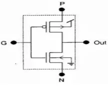
A. Morgenshtein described new design GDI cell that allows reducing delay, area and power dissipation [2], [3]. GDI cell consists of 3 inputs – G (common gate input of PMOS and NMOS). P (input to drain/source of PMOS). N (input to drain/source of NMOS).
P. Balasubramanian and J. John described MGDI cell that overcomes the drawbacks of GDI-cell. It extremely akin to GDI cell but the difference is that the bulk of both NMOS and PMOS are constantly fixed to GND and VDD, respectively
[4], [9].
Using traditional CMOS technology digital circuits occupy large area and number of transistor count that increase power dissipation [1], [6], [7]. But using MGDI technology, area and power consumptions are reduced.
The current paper is organized into 5 sections. Section 1 gives introduction. Section 2 gives description of GDI technique. Section 3 gives description of MGDI technique. Section 4 gives brief literature survey. Finally, the paper is concluded with section 5.
2. GDI TECHNIQUE
In first look GDI cell similar to CMOS inverter but GDI cell consists of 3 inputs – G (common gate input of PMOS and NMOS), P (input to drain/source of PMOS) and N (input to drain/source of NMOS).Bulks of both PMOS and NMOS are attached to their diffusion P, N to reduce bulk effect. GDI cell is shown in fig-1[3].
Fig-1: Basic GDI cell
GDI decreases both gate leakage current and sub threshold leakage current as compared to traditional CMOS. But its performance depreciates when used in and below 90nm technology. Fabrication of basic GDI cell is not possible in traditional p well progression. When substrate attached to drain, threshold voltage is increased and when the substrate is attached to source, body effect is destroyed in below equations [6].
(1)
‘Vth’stands for threshold voltage, VSB stands for
source body voltage, ‘Vtho’ stands for zero bias threshold
voltage, ‘γ’ stands for substrate bias coefficient, ‘ФF’ is fermi
potential, ‘VSB’ Source to substrate voltage, ‘VDS ‘drain to
© 2017, IRJET | Impact Factor value: 5.181 | ISO 9001:2008 Certified Journal | Page 875
3. MODIFIED GATE DIFFUSION INPUT TECHNIQUE
(MGDI)
MGDI is a new technique for designing low power digital circuits. This technique is adopted from GDI technique. MGDI technique is used to reduce power dissipation, transistor count and area of digital circuits. MGDI also consists of three input terminals - G, (input of both PMOS and NMOS) P, (input to drain/source of PMOS) and N (input to drain /source of NMOS) except the bulks of PMOS (SP) and NMOS (SN) are constantly coupled to VDD and
GND, respectively [5].
Fig-2: Basic MGDI cell
MGDI overcomes the drawbacks of GDI cell. With technology scaling, the influence of source body voltage on transistor threshold voltage gets exceeding abridged i.e. the linearized body coefficient ‘γ’ in below equation. Make MGDI pertinent in 65 nm technology and below [8].
On varying the values of G, P, N, SP and SN in MGDI
cell, SP and SN will remain constantly coupled to VDD and GND
[image:2.595.108.216.263.359.2]various functions are obtained, shown in the following table [5].
Table -1: Miscellaneous functions using MGI cell
G P N SP SN OUTPUT FUNCTION
A VDD 0 VDD 0 A’ INVERTER
B 0 A VDD 0 A.B AND
A B VDD VDD 0 A+B OR
B A A’ VDD 0 A’B+AB’ EX-OR
B A’ A VDD 0 AB+A’B’ EX-NOR
S A B VDD 0 AS’+BS 2:1 MUX
From table-1 it is noticed that different logic styles can be designed using one MGDI cell. OR gate and AND gate is designed using two transistors only, while in conventional
CMOS it requires 6 transistors. The main advantage of MGDI technique is that it reduces transistor counts and area on chip that’s cause of low power consumptions. So it is easy to design complex circuits using MGDI technique.
4. LITERATURE SURVEY
4.1 Full adder using MGDI cells
In the paper [6] full adder is implemented using MGDI cell. Full adder is a combinational circuit that has three inputs bits augend bit (A), addend bit (B) and carry bit (CIN) from previous stage and two outputs sum(S) and
carry out (COUT). Truth table of full adder is shown in
[image:2.595.328.539.316.520.2]table-2.
Table-2: Truth table of full adder
A B CIN Sum COUT
0 0 0 0 0
0 0 1 1 0
0 1 0 1 0
0 1 1 0 1
1 0 0 1 0
1 0 1 0 1
1 1 0 0 1
1 1 1 1 1
The Boolean expressions for Full adder are following [1]:
(2)
(3)
Now using MGDI cell full subtractor is designed. Logic circuit and schematic of designed full subtractor is shown below in fig-7.
[image:2.595.43.283.546.704.2] [image:2.595.314.543.668.748.2]© 2017, IRJET | Impact Factor value: 5.181 | ISO 9001:2008 Certified Journal | Page 876
Fig- 4: Schematic diagram of 1 bit full adderThe present work proposes the design of a full adder using modified Gate Diffusion Input (MGDI) and Mixed Threshold Voltage (MVT) scheme. The current work has been conceded in 45nm technology using HSPICE whereas the layout has been designed in Microwind. Evaluations with traditional CMOS transistors, transmission gate and CPL disclosed a decrease of 82.76%, 54.54% and 73.68% in number of transistors exploited, 93.33%, 72.79% and 86.39% in surface area, 54.18%, 58.37% and 52.44% in average power consumption, 62.27%, 49.08% and 79.85% in peak power consumption, 89.73%, 89.75% and 93.15% in delay time while a magnanimous 95.29%, 95.73% and 96.74% in power delay product, respectively. Plus, a vital decline of 99.52%, 99.56% and 99.78% in energy delay product is gained compared to a full adder realized embracing the popular CMOS logic, transmission gates as well CPL, successively [6].
Fig-5: Waveform of 1 bit full adder using MGDI cell
4.2 bit comparator using GDI cells
In paper [7] the magnitude comparator is a fundamental arithmetic component of digital system. A magnitude comparator is used in Digital Signal Processors (DSP) for data processing, microprocessor for decoding instruction and microcontroller for controlling temperature of furnace in industry. Comparator is a combinational circuit, N bit comparator compares two N bit binary numbers A and B. The block diagram of N bit comparator is follows in fig- 6. It generates three outputs that is denoted by A=B (F1), A<B
(F2), A>B (F3).
Fig-6: Block diagram of 2 bit comparator
Table-3 Truth table of 2 bit comparator
A1 A0 B1 B0 A=B(F1) A<B(F2) A>B(F3)
0 0 0 0 1 0 0
0 0 0 1 0 1 0
0 0 1 0 0 1 0
0 0 1 1 0 1 0
0 1 0 0 0 0 1
0 1 0 1 1 0 0
0 1 1 0 0 1 0
0 1 1 1 0 1 0
1 0 0 0 0 0 1
1 0 0 1 0 0 1
1 0 1 0 1 0 0
1 0 1 1 0 1 0
1 1 0 0 0 0 1
1 1 0 1 0 0 1
1 1 1 0 0 0 1
© 2017, IRJET | Impact Factor value: 5.181 | ISO 9001:2008 Certified Journal | Page 877
To determine whether A is greater than B or viceversa and then firstly check the most significant bit If most significant bit of both inputs is different, e.g. suppose most significant of A is 1 and most significant bit of B is 0 then A> B, if condition is reverse then A <B. If most significant bit of both the input is equal then go for next bit and then compare the next bit of both the input If both the inputs are same then A= B.The Boolean expressions for 2 bit comparator are following [7].
(4)
(5)
(6)
Now using GDI cell 2 bit comparator is designed. Schematic of designed 2 bit comparator is shown below in fig-7.
Fig-7: Schematic of 2 bit comparator using GDI cell
The performance of the proposed GDI magnitude comparator circuit with help of full adder logic has shown good performance in compare to existing conventional CMOS based design. The comparative performance of conventional CMOS and proposed GDI magnitude comparator with respect to power consumption at different range of input voltage, temperature and frequency has been discussed in the paper [7].
4.3 Full subtractor using GDI cell
In the paper [8] full subtractor is implemented using GDI cell. Full subtractor is a combinational circuit that has three inputs U (minuend), V (subtrahend), W (borrow from previous stage) and two outputs, one is D (difference) and another is B (Borrow).Truth table of full subtractor is shown below.
Table-4 Truth table of full subtractor
X Y Z D B
0 0 0 0 0
0 0 1 1 1
0 1 0 1 1
0 1 1 0 1
1 0 0 1 0
1 0 1 0 0
1 1 0 0 0
1 1 1 1 1
The Boolean expressions for Full subtractor are following [7]:
(7)
(8)
Now using GDI cell full subtractor is designed. Logic circuit and Schematic of full subtractor is shown below in fig-7 and fig-8.
Fig-8: logic circuit of full subtractor
© 2017, IRJET | Impact Factor value: 5.181 | ISO 9001:2008 Certified Journal | Page 878
Fig-10: Waveform of 1 bit full subtractor using GDI cellThe proposed design [8] of a full subtractor using Gate Diffusion Input (GDI) procedure which on simulation has been found to consume low power in conjunction with lesser delay time and fewer transistors while maintaining proper output-voltage swing. The present work has been performed in 150nm technology using Tanner SPICE and the layout has been concocted in Microwind. Comparisons with standard CMOS, transmission gate and CPL techniques showed a reduction of 72.00%, 63.16% and 58.82% in terms of transistor count, 99.68%, 88.78% and 99.99% in terms of average power consumption, 4.85%, 84.39% and 85.68% in terms of delay time and a significant 99.95%, 98.25 % and 99.99% in terms of power delay product, respectively [8].
Furthermore, a depreciation of 97.24%, 92.42% together with 95.10% in surface area is reaped when judged against a full subtractor composed adopting the popular CMOS approach, transmission gates and CPL, proportionately [8].
CONCLUSIONS
This paper work introduces the MGDI technique and implementation of various digital circuits using GDI technique and MGDI technique. Simulation is done in Comparison between conventional CMOS, GDI and MGDI technique is shown in the case of area, transistor count and static power consumptions. Using MGDI technique, implemented logic gates and digital circuits reduced to 25% - 90% in number of transistors and due to this area on chip decreases as well as significant reduction in power consumptions. Using MGDI technique various digital circuits can implement to increase efficiency of digital circuits.
REFERENCES
[1] M. Morris Mano and Michael D. Cilettie, "Digital Design,"
4'd ed., Prentice Hall, pp. 130_133, 146-149,144-146,2006.
[2] Sung-Mo Kang and Yusuf Leblebici, "CMOS Digital
Integrated Circuits- Analysis and Design," 3'd ed., Tata McGraw-Hill ed., pp. 47-80,117-133,481-482,2003.
[3] Arkadiy Morgenshtein, Alexander Fish and Israel A.
Wagner, “Gate-Diffusion Input (GDI): A Power-Efficient Method for Digital Combinatorial Circuits”, IEEE Transactions on Very Large Scale Integration (VLSI) Systems, Vol. 10, No. 5, October 2002.
[4] Arkadiy Morgenshtein, Idan Shwartz and Alexander
Fish. “Gate-Diffusion Input (GDI) logic in standard CMOS Nanoscale Process” IEEE 26th Convention of Electrical
and Electronics Engineers in Israel, pp.776 - 780 2010.
[5] Padmanabhan Balasubramanian and Johince John, “ Low
Power Digital design using modified GDI method”, International Conference on Design and Test of Integrated Systems in Nanoscale Technology, IEEE, pp.190-193, September 2006.
[6] Krishnendu Dhar, “ Design of a Low Power, High Speed,
Energy Efficient Full Adder Using Modified GDI and MVT Scheme in 45nm Technology”, IEEE, International Conference on Control, Instrumentation, Communication and Computational Technologies (ICCICCT) pp.36-41, July 2014.
[7] Vijaya Shekhawat, Tripti Sharma and Krishna Gopal
Sharma, “2-Bit Magnitude Comparator using GDI Technique”, IEEE International Conference on Recent Advances and Innovations in Engineering (ICRAIE-2014), pp. 1-5 May 2014.
[8] Krishnendu Dhar, Aanan Chatterjee, Sayan Chatterjee,
“Design of an Energy Efficient, High Speed, Low Power Full Subtractor Using GDI Technique”, Students' Technology Symposium IEEE, pp.199-204, February 2014.
[9] Krishnendu Dhar, “Design of a High Speed, Low Power
Synchronously Clocked NOR-based JK Flip-Flop using Modified GDI Technique in 45nm Technology”, IEEE International Conference on Advances in Computing, Communications and Informatics (ICACCI), September, 2014.
[10] Arkadiy Morgenshtein, Alexander Fish and Israel A.
Wagner, “An efficient implementation of D-flip flop using the GDI technique” ISCAS , pp. 673-676 May 2004.
[11] S. Ziabakhsh and M. Zoghi,“ Design of a Low-Power