High Voltage Input Rectifier Diode, 65 A
FEATURES
• Very low forward voltage drop
• Glass passivated pellet chip junction
• Designed and qualified according to
JEDEC
®- JESD 47
• Flexible solution for reliable AC power
rectification
• High surge, low V
Frugged blocking diode for DC charging
stations
• AEC-Q101 qualified P/N available (VS-65EPS12LHM3,
VS-65APS12LHM3)
• Material categorization: for definitions of compliance
please see
www.vishay.com/doc?99912
APPLICATIONS
• On-board and off-board EV / HEV battery chargers
• Renewable energy inverters
• Input rectification for single and three phase bridge
configurations
• Vishay Semiconductors switches and output rectifiers
which are available in identical package outlines
DESCRIPTION
High voltage rectifiers optimized for very low forward
voltage drop with moderate leakage.
These devices are intended for use in main rectification
(single or three phase bridge).
PRIMARY CHARACTERISTICS
IF(AV) 65 A
VR 800 V, 1200 V
VF at IF 1.12 V
IFSM 1000 A
TJ max. 150 °C
Package TO-247AD 2L, TO-247AD 3L Circuit configuration Single
TO-247AD 2L TO-247AD 3L
1
3
2
1
3 2
2
1 3
Base cathode
Anode Anode
Base cathode
2
1 3
Anode Cathode
VS-65APS..L-M3 VS-65EPS..L-M3
MAJOR RATINGS AND CHARACTERISTICS
SYMBOL CHARACTERISTICS VALUES UNITS
IF(AV) Sinusoidal waveform 65 A
VRRM 800, 1200 V
IFSM 1000 A
VF 30 A, TJ = 25 °C 1.0 V
TJ -40 to +150 °C
VOLTAGE RATINGS
PART NUMBERVRRM, MAXIMUM PEAK REVERSE VOLTAGE
V
VRSM, MAXIMUM NON-REPETITIVE PEAK REVERSE VOLTAGE
V
IRRM AT 150 °C
mA
VS-65EPS08L-M3 800 900
1.3
VS-65APS08L-M3 800 900
VS-65EPS12L-M3 1200 1300
1.3
VS-65APS12L-M3 1200 1300
ABSOLUTE MAXIMUM RATINGS
PARAMETER SYMBOL TEST CONDITIONS VALUES UNITS
Maximum average forward current IF(AV) TC = 121 °C, 180° conduction half sine wave 65
A Maximum peak one cycle
non-repetitive surge current IFSM
10 ms sine pulse, rated VRRM applied 840 10 ms sine pulse, no voltage reapplied 1000
Maximum I2t for fusing I2t 10 ms sine pulse, rated VRRM applied 3530 A2s 10 ms sine pulse, no voltage reapplied 5000
VS-65EPS..L-M3, VS-65APS..L-M3
www.vishay.com
Vishay Semiconductors
Revision: 06-Jul-2018 2 Document Number: 95998
For technical questions within your region: [email protected], [email protected], [email protected] Fig. 1 - Current Rating Characteristics Fig. 2 - Current Rating Characteristics
ELECTRICAL SPECIFICATIONS
PARAMETER SYMBOL TEST CONDITIONS VALUES UNITS
Maximum forward voltage drop VFM 65 A, TJ = 25 °C 1.12 V
Forward slope resistance rt
TJ = 150 °C
3.98 m
Threshold voltage VF(TO) 0.74 V
Maximum reverse leakage current IRM
TJ = 25 °C
VR = rated VRRM
0.1
mA
TJ = 150 °C 1.3
THERMAL - MECHANICAL SPECIFICATIONS
PARAMETER SYMBOL TEST CONDITIONS VALUES UNITS
Maximum junction and storage temperature range TJ, TStg -40 to +150 °C Maximum thermal resistance, junction to case RthJC DC operation 0.25
°C/W
Maximum thermal resistance, junction to ambient RthJA 40
Typical thermal resistance, case to heatsink RthCS Mounting surface, smooth, and greased 0.25
Approximate weight 6 g
0.21 oz.
Mounting torque minimum 6 (5) kgf · cm
(lbf · in)
maximum 12 (10)
Marking device
Case style TO-247AD 2L 65EPS08L
Case style TO-247AD 3L 65APS08L
Case style TO-247AD 2L 65EPS12L
Case style TO-247AD 3L 65APS12L
90 100 110 120 130 140 150
0 10 20 30 40 50 60 70
M
a
x
. A
llo
w
a
b
le C
a
s
e
T
e
m
p
er
at
u
re
(
°
C)
Average On-State Current (A) RthJC(DC) = 0.25 °C/W
30° 60°
90° 120°
180°
Conduction angleØ
80 90 100 110 120 130 140 150
0 20 40 60 80 100 120
Ma
x. Allow
a
ble
Ca
se
Te
mpe
ra
ture
(°C)
Average On-State Current (A) 30°
60° 90°
120° 180°
DC RthJC (DC) = 0.25 °C/W
Ø Conduction angle
Fig. 3 - Forward Power Loss Characteristics
Fig. 4 - Forward Power Loss Characteristics
Fig. 5 - Maximum Non-Repetitive Surge Current
Fig. 6 - Maximum Non-Repetitive Surge Current
Fig. 7 - Forward Voltage Drop Characteristics 0
10 20 30 40 50 60 70 80 90 100
0 10 20 30 40 50 60 70
Ma
x. Ave
ra
g
e On
-S
ta
te
Pow
e
r Loss
(W)
Average On-State Current (A) 180°
120° 90° 60° 30°
RMS limit
Conduction angle TJ = 150 °C
Ø
0 20 40 60 80 100 120 140
0 20 40 60 80 100 120
Ma
x. Ave
ra
g
e
On-st
a
te
Pow
e
r Loss
(W)
Average On-state Current (A) 180°
120° 90° 60° 30°
RMS limit
DC
TJ= 150 °C
Ø Conduction angle
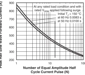
At any rated load condition and with rated VRRM applied following surge.
Initial TJ = 150 °C
at 60 Hz 0.0083 s at 50 Hz 0.0100 s
Peak Half Sine Wave Forward Current (A) Number of Equal Amplitude Half
Cycle Current Pulse (N)
10 100
1 200 300 500 700
400 600 800 900
Peak Half Sine Wave Forward Current (A)
Pulse Train Duration (s)
1.0 0.1
0.01 100 400 600 800 1000 1100
Maximum non-repetitive surge current versus pulse train duration. Initial TJ = 150 °C
No voltage reapplied Rated VRRM reapplied
10 900
700
500
300 200
Instantaneous Forward Current (A)
Instantaneous Forward Voltage (V)
0 0.5 1.0 1.5 2.0 2.5 3.0 3.5 4.0 4.5 1
10 1000
100
TJ = 150 °C
VS-65EPS..L-M3, VS-65APS..L-M3
www.vishay.com
Vishay Semiconductors
Revision: 06-Jul-2018 4 Document Number: 95998
For technical questions within your region: [email protected], [email protected], [email protected] Fig. 8 - Thermal Impedance ZthJC Characteristics
ORDERING INFORMATION TABLE
ORDERING INFORMATION
(Example)
PREFERRED P/N QUANTITY PER T/R MINIMUM ORDER QUANTITY PACKAGING DESCRIPTION
VS-65EPS08L-M3 25 500 Antistatic plastic tubes
VS-65APS08L-M3 25 500 Antistatic plastic tubes
VS-65EPS12L-M3 25 500 Antistatic plastic tubes
VS-65APS12L-M3 25 500 Antistatic plastic tubes
LINKS TO RELATED DOCUMENTS
Dimensions TO-247AD 2L www.vishay.com/doc?95536
TO-247AD 3L www.vishay.com/doc?95626
Part marking information TO-247AD 2L www.vishay.com/doc?95648
TO-247AD 3L www.vishay.com/doc?95007 ZthJ
C
- Tra
nsie
nt
The
rma
l
Impe
d
an
ce
(
°
C/W
)
Square Wave Pulse Duration (s) 0.001
0.01 0.1 1
0.0001 0.001 0.01 0.1 1 10
0.17
Single Pulse 0.5 0.33
0.08 0.25
Steady state value (DC operation)
2
-
Current rating (65 = 65 A)
3
-
Circuit configuration:
4
-
Package:
5
-
Type of silicon:
6
-
Voltage code x 100 = V
RRME = single, 2 pins
A = single, 3 pins
P = TO-247AD
S = standard recovery rectifier
12 = 1200 V
08 = 800 V
Device co
d
e
6
2
3
4
5
7
65
E
P
S
12
L
8
-M
3
V
S
-1
1
-
Vi
s
hay
S
emiconductor
s
product
Environmental digit:
-M3 = halogen-free, RoH
S
-compliant, and termination
s
lead (Pb)-free
7
-
L = long leads
www.vishay.com
Vishay Semiconductors
TO-247AD 2L
DIMENSIONS
in millimeters and inches
Notes
(1) Dimensioning and tolerancing per ASME Y14.5M-1994 (2) Contour of slot optional
(3) Dimension D and E do not include mold flash. These dimensions are measured at the outermost extremes of the plastic body (4) Thermal pad contour optional with dimensions D1 and E1
(5) Lead finish uncontrolled in L1
(6) Ø P to have a maximum draft angle of 1.5 to the top of the part with a maximum hole diameter of 3.91 mm (0.154") (7) Outline conforms to JEDEC® outline TO-247 with exception of dimension A min., D, E min., Q min., S, and note 4
SYMBOL MILLIMETERS INCHES NOTES SYMBOL MILLIMETERS INCHES NOTES
MIN. MAX. MIN. MAX. MIN. MAX. MIN. MAX.
A 4.65 5.31 0.183 0.209 E 15.29 15.87 0.602 0.625 3 A1 2.21 2.59 0.087 0.102 E1 13.46 - 0.53
-A2 1.50 2.49 0.059 0.098 e 5.46 BSC 0.215 BSC b 0.99 1.40 0.039 0.055 Ø K 0.254 0.010 b1 0.99 1.35 0.039 0.053 L 19.81 20.32 0.780 0.800 b2 1.65 2.39 0.065 0.094 L1 3.71 4.29 0.146 0.169 b3 1.65 2.34 0.065 0.092 Ø P 3.56 3.66 0.14 0.144 c 0.38 0.89 0.015 0.035 Ø P1 - 6.98 - 0.275 c1 0.38 0.84 0.015 0.033 Q 5.31 5.69 0.209 0.224 D 19.71 20.70 0.776 0.815 3 R 4.52 5.49 0.178 0.216 D1 13.08 - 0.515 - 4 S 5.51 BSC 0.217 BSC D2 0.51 1.35 0.020 0.053
0.10MCAM
E
(2)
(3)
(4)
(4) (2) R/2
B
2 x R
S
D
See view B
2 x e 2 x b
2 x b2
L C
(5) L1
1, 2 3
Q
D A
A2 A
A
A1 C
Ø KMDBM
A
(6) F P (Datum B)
F P1
D1 (4)
4
E1 0.01MDBM
View A - A Thermal pad
D2
D D
C C
View B (b1, b3)
Base metal
c1
(b, b2)
Section C - C, D - D (c)
Legal Disclaimer Notice
www.vishay.com
Vishay
Revision: 08-Feb-17 1 Document Number: 91000