An 8-Bit Current-Mode Folding ADC with
Optimized Active Averaging Network
M. Azin
and M. Sharif Bakhtiar
1In this paper, an 8-bit CMOS current-mode folding-interpolating ADC is presented. A new active averaging-interpolating network is described, which results in a better error correction factor compared to its resistive counterpart. Using novel circuits for fast settling and careful transistor sizing, a fast (>160 Msps) and low power (70 mW in 2.5 V supply voltage) 8-bit ADC, with a total chip area of 1 1:4 mm in a 0.25 micron CMOS process, is demonstrated.
INTRODUCTION
The increasing demand for digital processing systems makes high-speed and low-voltage analog to digital converters key elements in many applications, such as wireless digital communication and video process-ing. CMOS ash ADCs can satisfy the high speed requirement. However, the complexity and, conse-quently, the power consumption of ash ADCs grow exponentially as resolution increases. This is why ash converters are only used for low-resolution (6-7 bits) applications [1,2]. Pipeline ADCs are used for many high-speed applications, which require a higher resolution. Pipeline ADCs, nonetheless, introduce an inherent latency, which makes them unsuitable for applications such as control and data storage. The folding-interpolating technique is an alternative that avoids the complexity of ash ADCs. Folding ADCs can also achieve high-speed, high-resolution and low power characteristics, as well as a low latency [3-5].
Cross-connected dierential pairs are used to fold the input signal of the ADC [6]. The number of dierential pairs is referred to as the folding factor. To achieve a higher resolution, a larger folding fac-tor is needed, which, in turn, results in a larger capacitive load at the output nodes of the folding blocks. Moreover, the low oset requirement for the dierential input pairs directly translates to large input
*. Corresponding Author, Department of Electrical Engi-neering and Computer Science, Case Western Reserve University, Cleveland, Ohio, USA.
1. Department of Electrical Engineering, Sharif University of Technology, Tehran, I.R. Iran.
devices, which, in turn, slow down the circuit. On the other hand, the signal frequency at the folder's output is higher than the input frequency by an amount proportional to the folding factor. This is why the output nodes of the folding blocks dramatically limit the speed of a folding-interpolating ADC at higher resolutions. The application of an OTA at the output of the folders can improve the ADCs bandwidth eec-tively [4]. However, this approach is not well suited for low voltage applications.
In this work, a novel low voltage method to improve the speed and the settling time of the folding blocks is presented. A new structure for oset averag-ing is also presented. Unlike resistive oset averagaverag-ing structures [3], the proposed structure can be used in current mode circuits and results in a better Error Correction Factor (ECF).
System level considerations of the converter and the designed architecture are given in the following section. Then, a new active averaging network is presented, which is compared to conventional averaging networks and, circuit implementation of the ADC is described. Post layout simulation results and the conclusion are presented, respectively, in the nal sections.
ARCHITECTURE
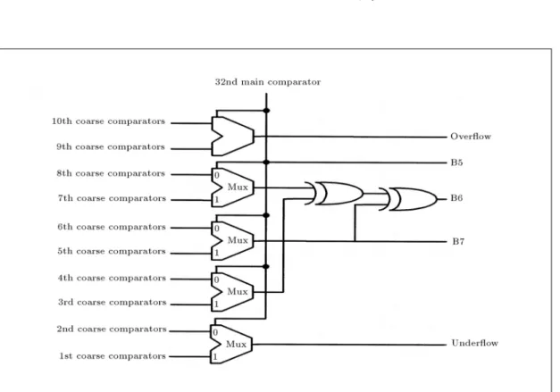
Because of the longer delay time of multistage architec-tures, a single stage architecture is selected for the ADC implementation. As shown in Figure 1, four folding blocks are used to make 32 zero crossing points and the folding factor is selected to be 8.
Figure 1. Proposed Single stage ADC.
the 4 dierential outputs of the folding blocks are fed into an interpolating network, resulting in 32 folded signals. As described in the next section, interpolation and averaging networks are implemented using current mirrors. To detect the zero crossing points of 32 folded signals, 32 current comparators are used. While bit 0 (LSB) to bit 5 are derived in the main path, ten additional comparators are also used in the coarse ADC path to produce the two most signicant bits (B7 and B6), as well as overow and underow bits. As shown
signicant bits and the others are used to provide underow and overow signals.
OFFSET AVERAGING
Averaging is an eective mean to reduce oset induced errors. First order resistive networks are typically used for oset averaging, where outputs of the folding blocks are interconnected through a resistive network (Figure 3). The averaging network may also be used for interpolation of the folded signals. In Figure 3, the load resistance of the folding blocks, represented by resistors R0s and R1s, are interpolating-averaging resistors.
In an oset averaging network, each output is a linear combination of input signals. Therefore, if Sini
and Soutirepresent the input and output signals of the
network, respectively, it can be shown that: Sout0=
M 1X i=0
hi:Sini; (1)
Figure 3. First order resistive averaging network.
where M is the number of total input signals of the averaging network and h0
is are oset averaging factors.
Suppose that M input signals of an averaging network are sorted such that zero crossing points of Sink are
between the zero crossing points of Sink+1and Sink 1,
then it can be shown that: Sini= SinM
2+i for 0 i
M
2 1: (2)
Equation 2 means that the second half of each input signal has the opposite polarity of the corresponding rst half. If Sin0has a zero value, then it can be written
that:
Sini= SinM i for i 6= 0: (3)
Using Equation 3 leads to:
hi= hM i for i 6= 0: (4)
Errors in the input blocks of a folding-interpolating ADC can be divided into vertical and horizontal er-rors [3]. An averaging network improves these erer-rors in the following ways:
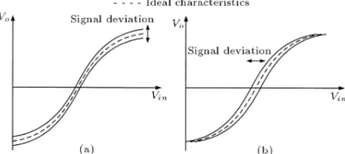
1. Vertical error: This is shown in Figure 4a, where Vin is the input voltage to the ADC and Vo is the output signal of a folding block. Vertical error is caused by deviation of the folding characteristic curve away from the ideal characteristic in the Vo direction. A mismatch of the tail current sources
Figure 4. (a) Vertical error; (b) Horizontal error.
in a folding block is a cause of vertical error, which remains constant when the input signal of the ADC is changing;
2. Horizontal error: This is the deviation of the characteristic curve in the Vin direction from the ideal characteristic (Figure 4b). One major source of horizontal error is the mismatch in the folder pairs. In contrast to vertical errors, horizontal errors depend on the input value. Since the maximum slope occurs at the zero crossing points of the folding characteristic, horizontal error has its maximums at these points. Conversely, the lowest value of the horizontal error occurs when the output signal is at its extreme. This is shown in Figure 5, where e is the horizontal error normalized to its maximum.
ECF (Error Correction Factor) is dened as the eective error at the input of an averaging network to the output error, i.e.:
ECF = Sin:Goa
Sout ; (5)
where Sin and Sout are the errors at the input and
output of the averaging network, respectively, and Goa is the averaging gain. With respect to Equation 1, it
Figure 5. Horizontal error has its largest value at zero crossing points and its lowest at maximums and minimums.
Sout0
i=0
i 2+i 5 :Sin0
And, for the horizontal error, one can write: 2 Sout0= 2 4 M 2 1 X i=0
hi hM 2+i
2
:e2 i
3 5 :2
Sin0; (8)
where ei is the value of e for Sini, when Sin0 is
zero. It can be shown that e0 is equal to 1 and
other ei's are less than 1. Goa can be obtained by
dierentiating Equation 1. Substituting Equations 7 and 8 in Equation 5 determines ECFs for vertical and horizontal errors as follows:
ECFVE= Goa:
2 4 M 2 1 X i=0
hi hM 2+i 2 3 5 1=2 ; (9)
for vertical errors; ECFHE= Goa:
2 4 M 2 1 X i=0
hi hM 2+i 2 :e2 i 3 5 1=2 ; (10) for horizontal errors.
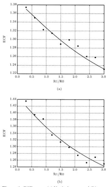
A resistive averaging network was rst designed for the ADC. ECF was then calculated for dierent values of R1/R0 using Equations 9 and 10. The results
are compared with those of Monte Carlo simulations in Figure 6.
Equation 1 can be implemented by current mir-rors, as shown in Figure 7. For component and area saving, this network can also be employed as an active interpolating network. Averaging factors are determined by optimizing the ECF equations; this is why the circuit is denoted as an optimum averaging network. The optimization of Equation 10 results in the addition of 1
3 of each input signal to its two
neighboring signals, in order to make an output signal. Using a Monte Carlo simulation, it is shown that the optimum averaging network improves vertical errors by a factor of 1.3 and horizontal errors by a factor of 1.5. For the rst order resistive averaging network, the above improvement with the same Goa would be limited to 1.2 for vertical errors and 1.3 for horizontal errors.
Figure 6. ECF versus (a) Vertical errors and (b) Horizontal errors. Circles are Monte Carlo simulation results.
Figure 7. Current mode averaging network.
CIRCUIT IMPLEMENTATION Folding Blocks
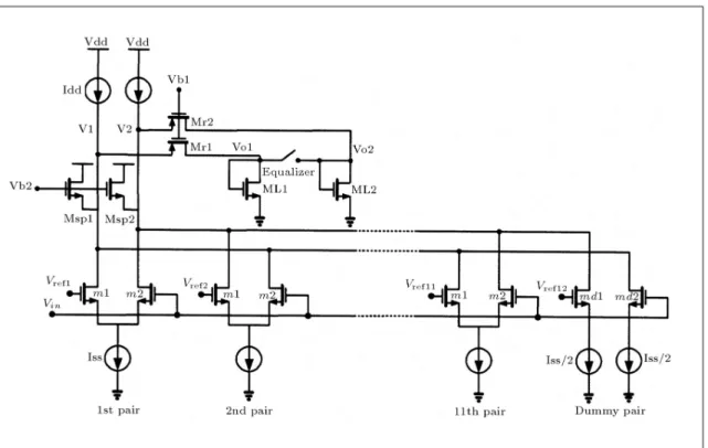
Figure 8 shows the circuit of a folding block. Among eleven used dierential pairs, eight (3rd to 10th) are the main folders, two (2nd and 11th) are to enhance the range for interpolation and one (1st) is added for the DC balance. The output currents of the
Figure 8. Folding block circuit.
11 dierential pairs and a dummy pair are added together to make two folded currents. These currents are subtracted from two constant currents and, then, ow through the cascoded transistors, Mr1 and Mr2. The two output currents are fed into the current mirror transistors (ML1 and ML2), which drive the interpolating/averaging network. In order to increase the speed of the output nodes, an equalizing switch shorts these nodes to each other for about 1/3 of the clock period.
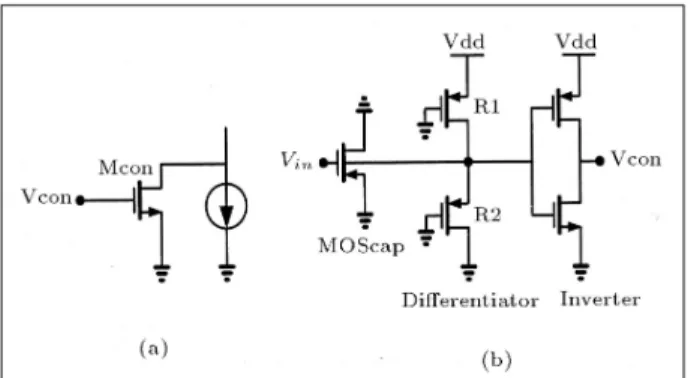
Two novel methods are used to speed up the folder response to large input signals:
1. Large positive input enhancements: For large pos-itive input pulses, the common mode voltage of V1 and V2 falls (Figure 8), turning Mr1 and Mr2 o. In order to improve the common mode voltage settling, two NMOS transistors (Msp1 and Msp2) are added to the circuit. Vb2 is set at one threshold voltage above the common mode voltage of V1 and V2. When the voltage at these nodes decreases, due to a positive input, Msp1 and Msp2 turn on, in order to speed up the folding block settling. 2. Large negative input enhancements: A dierential
pair, with single ended input, shows a slower response to falling input than to rising input. This is because the tail node, where the source of the two input devices are connected together, has a slew rate limited behavior for a falling input. Tail settling, for rising and falling inputs, is compared
in Figure 9. To improve ADC speed with a falling input pulse, additional current sources are paral-leled with each tail current source (Figure 10a). These additional current sources turn on when a falling input pulse is detected. The detector circuit, which consists of a dierentiator and an inverter, is shown in Figure 10b. As shown in Figure 11, a considerable improvement is achieved, due to the injection of the current pulses through the additional current sources.
The nite output resistance of the tail current sources results in an input-dependent current oset in the output signals of a folding block. The input dependency of this oset is due to the fact that for a dierential pair with Vin < Vref, the current
source voltage is constant and for Vin > Vref, the
source voltage follows the input signal. The variation
Figure 10. (a) Additional current source; (b) Falling input detector.
Figure 11. The eect of additional current sources and falling input detector.
Figure 12. Error induced by current source nite resistance.
of output oset with the input voltage is shown in Figure 12 (dotted line), where VFS is the full input
range voltage and RCS is the current source output
resistance.
To compensate for the current error, the input voltage is applied to a dummy pair, with:
Rcs dummy = 2:Rcs;
nonlinear behavior of the current source resistance, this improvement is limited to a factor of 5.
Comparators
Current comparators are used to detect the zero cross-ing point of 32 folded signals. Because of the pamplication of signals in the folding blocks, the re-quirements for comparators in the folding-interpolating ADCs are fairly relaxed. The designed current com-parator is shown in Figure 13.
The two input signals are subtracted from two constant currents and then ow into the bistable circuit (M1 M4). When Veq goes low, the bistable circuit
switches to one of the two stable states, according to the dierence of the input currents. It can be shown that, if ICChas a value slightly larger than the common
mode value of the input currents, the mismatch of M1 and M2 has a negligible eect on the comparator oset. As ICC increases, the eect of the M1 and M2
mismatch becomes more dominant. In order to have a precise comparator, ICC should be as close to the
common mode value of the inputs as possible. On the other hand, a small value of dierence between ICC and the common mode value results in a large
settling time for the bistable circuit. In order to have precision and speed simultaneously, two transistors (M5 and M6) turn on shortly (1 nsec) after Veq goes low. This will cause a higher current ow into the bistable circuit and push the bistable faster towards its nal state. A careful transistor sizing leads to a 1uA current oset and 1 nsec comparison time for the comparators.
ADC IMPLEMENTATION
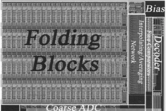
The ADC was implemented in a 0.25 m digital CMOS process with one poly and ve metal interconnection levels. The designed layout measured 1 1:4 mm2,
excluding the reference ladder. The chip layout is shown in Figure 14. Because of the matching and output resistance requirements, the tail current sources are responsible for the large area occupied by the folding blocks.
Monte Carlo simulations show the maximum INL and DNL values of 0.7 LSB and 0.5 LSB, respec-tively (Figure 15). Taking the extracted parasitic into account, the dynamic performance of the ADC was simulated, based on the assumption of a 10-bit resolution and a 2.5 nsec settling time for the front-end track and hold circuit.
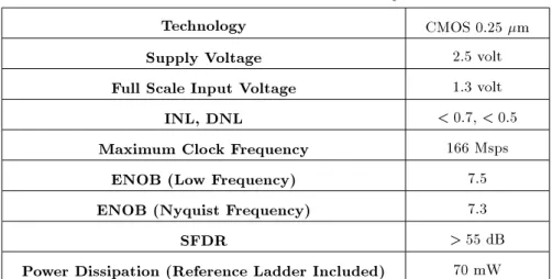
The output spectrum for a full-scale sinusoidal input signal is shown in Figure 16. Table 1 shows the overall performance and specication of the ADC,
Figure 14. Chip layout.
Figure 15. (a) INL error; (b) DNL error.
Figure 16. Output spectrum, input frequency = 16.27 MHz, clock frequency = 166.6 MHz.
ENOB (Nyquist Frequency) 7.3 SFDR > 55 dB Power Dissipation (Reference Ladder Included) 70 mW
Table 2. Performance comparison of recent works.
Author Date Bits Speed (Msps) Power (mW) [8] 2001 8b 100 165 [9] 2003 8b 300 200 [10] 2001 8b 30 18 [11] 2004 8b 600 200 [12] 1997 12b 60 300 [13] 1996 8b 80 80 This work - 8b 166 55
based on the post layout simulations. The performance parameters of this work are compared with other similar ADCs in Table 2.
CONCLUSION
The design of a high-speed, 8-bit folding-interpolating ADC was presented. A new optimized current mode interpolating and averaging method was used. It was shown that the presented current mode interpolating and averaging technique results in a higher degree of error correction compared to the conventional resis-tive method. The use of novel speed enhancement techniques provided the possibility of increasing the sampling frequency to more than 160 MHz with an SFDR better than 55 dB.
REFERENCES
1. Tsukamoto, S., Endo, T. and Schoeld, W. \A CMOS 6-b 400-MSample/s ADC with error correction", IEEE J. Solid-State Circuits, 33, pp 1939-1947 (Dec. 1998). 2. Tamba, Y. and Yamakido, K. \A CMOS 6-b
500-MSample/s ADC for a hard disk driver read channel", in ISSCC Dig. Tech. Papers, pp 324-325 (Feb. 1999). 3. Pan, H., Segami, M., Choi, M., Cao, J., Hatori, F.
and Abidi, A. \A 3.3V, 12b, 50MS/s A/D converter in 0.6-um CMOS with over 80dB SFDR", in ISSCC Dig. Tech Papers, pp 40-41 (Feb. 2000).
4. Nauta, B. and Venes, A.G.W. \A 70-MS/s 100-mW 8-b CMOS folding and interpolating A/ D converter", IEEE J. Solid-State Circuits, 30, pp 1302-1308 (Dec. 1995).
5. Pan, H. \A 3.3-Volt 50-MS/s A/D converter in 0.6um CMOS with 80-dB SFDR", PhD Thesis, University of California, Los Angeles (1999).
6. Razavi, B., Principles of Data Conversion System Design, New York, IEEE Press (1995).
7. van de Plassche, R.J. and Baltus, P. \An 8-bit 100-MHz full-Nyquist analog-to-digital converter", IEEE J. Solid-State Circuits, 23, pp 1334-1344 (Dec. 1988). 8. Choe, M.J., Song, B.S. and Bacrania, K. \An 8-bit 100MSample/s CMOS pipelined folding ADC", IEEE J. Solid-State Circuits, 36(2), pp 184-194 (Feb. 2001). 9. Li, Y. and Sanchez-Sinencio, E. \A wide input band-width 7-bit 300MSample/s folding and current-mode
interpolating ADC", IEEE J. Solid-State Circuits, 38(8), pp 1405-1410 (Aug. 2003).
10. Sigenobu, T. et al. \A 8-b 30MS/s 18mW ADC with 1.8-V single power supply", Proc. Symp. VLSI Circuits, pp 209-210 (2001).
11. Geelen, G. and Paulus, E. \An 8b 600MS/s 200mW A/D converter using an amplier preset technique" IEEE International Solid-State Conference (Feb. 2004).
12. Vorenkamp, P. and Roovers, R. \A 12-b, 60-M Sam-ple/s cascaded folding and interpolating ADC", IEEE J. Solid-State Circuits, 32, pp 1876-1886 (Dec. 1997). 13. Venes, A.G.W. and van de Plassche, R.J. \An 80-MHz, 8-b CMOS folding A/D converter with dis-tributed track and hold preprocessing", IEEE J. Solid-State Circuits, 31, pp 1846-1853 (Dec. 1996).