Direct Imaging of Ultrafast Charge Carrier Dynamics in Semiconducting Nanowires Using Two-Photon Excitation and Spatially-Separated Pump-Probe Microscopy
Justin Robert Kirschbrown
A dissertation submitted to the faculty of the University of North Carolina at Chapel Hill in partial fulfillment of the requirements for the degree of Doctor of Philosophy in the
Curriculum in Materials Science and Engineering.
Chapel Hill
2013
ii © 2013
iii ABSTRACT
Justin Kirschbrown: Direct Imaging of Ultrafast Charge Carrier Dynamics in Semiconducting Nanowires Using Two-Photon Excitation and Spatially-Separated
Pump-Probe Microscopy
(Under the direction of Dr. John M. Papanikolas)
iv
v
vi
ACKNOWLEDGEMENTS
First of all, I would like to express my deepest gratitude to my advisor Dr. John Papanikolas for his invaluable input and advice on topics not only concerning science, but also life in general. I would also like to thank Dr. Ralph House and Dr. Brian Mehl for their initial development of the microscope, and for taking me under their wings when I first joined the Papanikolas group. Their instruction and friendship were of the utmost importance to my success. I would like to thank Michelle Gabriel for her collaboration on these projects, and for helping to make the oft mundane task of data collection entertaining. I would also like to thank the other members of the Papanikolas group, past and present; especially Stephanie Bettis, Dr. Erik Grumstrup, Emma Cating, Scott Barnes, Chuan Zhang, Dr. David Zigler, and Dr. Kyle Brennaman. Additional recognition is required for Dr. James Cahoon and his research group, for providing silicon nanowire samples and helping me to better understand their growth process. I consider myself very fortunate to have had the pleasure to work with such wonderful people.
vii
TABLE OF CONTENTS
CHAPTER 1. INTRODUCTION... 1
CHAPTER 2. EXPERIMENTAL ... 3
2.1. MICROSCOPE LAYOUT ... 3
2.2. INSTRUMENT MANAGEMENT PLATFORM (IMP)SOFTWARE ... 7
2.2.1. Overview ... 7
2.2.2. Object Oriented Software ... 8
2.2.2.1. Class Inheritance ... 10
2.2.2.2. Handle Versus Value Objects ... 13
2.2.2.3. Relating These Concepts to IMP ... 14
2.2.3. Software Class Layout ... 16
2.2.3.1. Framework Object ... 17
2.2.3.2. Equipment and Equipment Component Objects... 18
2.2.3.3. Data Objects ... 28
2.2.3.4. Experiment Component Objects ... 31
2.2.4. Experiment Objects ... 34
2.2.4.1. Methods for Experiment Class Design ... 36
2.2.4.2. The Collect_Point and Collect_Line Methods ... 36
2.2.4.3. The Collect_Scan_Line Method ... 38
2.2.4.4. Single-Axis Scanning Experiment ... 39
2.2.4.5. Two-Axis Imaging Experiment ... 41
viii
CHAPTER 3. HYBRID STANDING WAVE AND WHISPERING GALLERY MODES IN NEEDLE-SHAPED ZNO RODS: SIMULATION OF EMISSION MICROSCOPY IMAGES USING FINITE DIFFERENCE FREQUENCY
DOMAIN METHODS WITH A FOCUSED GAUSSIAN SOURCE ... 43
3.1. ABSTRACT ... 43
3.2. BACKGROUND ... 43
3.3. EXPERIMENTAL... 45
3.4. RESULTS AND DISCUSSION ... 47
3.5. STANDING-WAVE AND WHISPERING GALLERY MODE DESCRIPTIONS ... 50
3.5.1. Finite Difference Frequency Domain (FDFD) Simulations ... 53
3.5.2. Implications ... 63
3.6. CONCLUSIONS ... 63
3.7. ACKNOWLEDGEMENT ... 64
CHAPTER 4. DIRECT IMAGING OF FREE CARRIER AND TRAP CARRIER MOTION IN SILICON NANOWIRES BY SPATIALLY-SEPARATED FEMTOSECOND PUMP–PROBE MICROSCOPY ... 65
4.1. ABSTRACT ... 65
4.2. BACKGROUND ... 65
4.3. EXPERIMENTAL... 66
4.4. RESULTS AND DISCUSSION ... 68
4.5. CONCLUSIONS ... 80
4.6. ACKNOWLEDGEMENT ... 80
CHAPTER 5. ANALYSIS OF RECOMBINATION MECHANISMS IN HIGHLY DOPED SILICON NANOWIRES ... 81
5.1. ABSTRACT ... 81
5.2. BACKGROUND ... 81
5.3. EXPERIMENTAL... 83
5.4. RESULTS AND DISCUSSION ... 86
5.4.1. Auger Recombination ... 87
ix
5.4.3. Thermal Oxide Nanowires ... 91
5.4.4. Hydrogen Annealed Nanowires... 93
5.5. CONCLUSIONS ... 98
CHAPTER 6. CONCLUSIONS ... 99
x
LIST OF TABLES
Table 1: Monochromator class summary. ... 21
Table 2: DAQ class summary. ... 23
Table 3: Channel class summary. ... 24
Table 4: Stage class summary. ... 26
Table 5: Axis class summary. ... 27
Table 6: Figure and Image class summary. ... 30
Table 7: Buffer class summary. ... 32
Table 8: Mask class summary. ... 33
Table 9: Experiment class summary. ... 35
Table 10: Parameters used to fit kinetics derived from pump-probe microscopy to a sum of three exponentials, ΔI(t)=A1e -t/τ1 + A2e -t/τ2 + A3e -t/τ3 ... 70
Table 11: Calculated Auger Recombination Decay Constants For Relevant Laser Powers. ... 89
Table 12: Averaged Fitting Parameters For the Native Oxide Sample. ... 87
Table 13: Averaged Fitting Parameters For the Thermal Oxide Sample. ... 93
xi
LIST OF FIGURES
Figure 1: Schematic of the spatially-separated pump probe microscope. ... 4
Figure 2: Schematic of the operation of the x-y beam scanner. ... 5
Figure 3: Demonstration of classes and objects. The “Dog” class is shown on the
left and provides a template for the object “Spot”. ... 9
Figure 4: Demonstration of the concept of inheritance. The child classes (c_Pointer and c_Pitbull) inherit properties and methods from the parent class (p_Dog). The Size property and the Speak method are uniquely
defined in each child class. ... 11
Figure 5: Demonstration of MATLAB handle and value classes with a switch object. State changes are linked in all copies of handle objects, but
independent in value classes. ... 14
Figure 6: Inheritance relationship for the monochromator equipment type object. The p_Monochrom parent class defines the functions that are required of the child classes, while the child classes dictate how a particular instrument
executes the commands. ... 15
Figure 7: Layout of the organizational structure of classes in the software. Each
class type plays an important role in the execution of the experiments... 16
Figure 8: Class layout for the Framework class. ... 17
Figure 9: Class layout for the parent Monochromator class. ... 20
Figure 10: Class layout for the DAQ and Channel objects. Channel objects are
housed inside of the DAQ object in the channel property. ... 22
Figure 11: Class layout for the Stage and Axis objects. Axis objects are housed
inside of the Stage object in the channel property. ... 25
Figure 12: Data types in the IMP software. Depending on the experiment to be conducted the data complexity can continue to grow in the future, which the
software would support. ... 28
Figure 13: Class layout for the Figure and Image objects. The Image class
inherits properties and methods from Figure class. ... 29
Figure 14: Class layout for the Buffer and Mask experiment component classes. ... 31
xii
Figure 16: Data processing procedure for a DAQ Channel object configured for counting (TOP) and configured for continuous analog acquisition (BOTTOM). The procedure shown is the same for collect_point and
collect_line methods, differing only by the number of points collected. ... 37
Figure 17: Data processing procedure for the collect_line_scan method. This is a continuous analog data acquisition method, which registers the coordinates
of the data after collection has completed. ... 39
Figure 18: Diagram showing the layout of the most commonly used experiment classes. Also shown are the objects contained in the properties of the
experiment classes. The symbols are defined in the legend on the left side. ... 40
Figure 19: (A) Diagram of the two-photon emission microscope. The 730 nm output of a mode-locked Ti:Sapphire laser is directed onto the back aperture of the microscope objective (50x, 0.8 NA) and focused to a diffraction-limited spot at the sample. Imaging is achieved by raster scanning the sample stage across the focused laser spot and monitoring the emission collected by the objective with a scanning monochromator/PMT. (B) Two-photon emission image of a 100 nm quantum dot with 810 nm excitation. The size of the emission feature suggests that the lateral resolution at this
wavelength is approximately 410nm. ... 47
Figure 20: (A) SEM image and (B) emission spectrum of a tapered zinc oxide nanorod. The red circle and double-headed arrow indicate the location at which the spectrum was acquired and the direction of the excitation polarization vector, respectively. (C-D) Photoluminescence images taken at 390 nm and 550 nm, respectively, show a modulated emission pattern along the structure. The lower case letters in (C) indicate the resonance spots
discussed in the text. ... 48
Figure 21: (A) Facet spacing determined from the SEM image in Figure 20A plotted as a function of position along the rod. (B) Intensity profiles obtained by integrating a column of pixels at each longitudinal position along the images for both the band-edge and trap emission images (Figure 20C and Figure 20D). The calculated whispering gallery mode locations for 730 nm and 390 nm light are indicted by the two brackets positioned between (A) and (B). The lower-case letters in the band-edge profile
correspond to the resonance spots indicated in Figure 20B. ... 51
Figure 22: (A) Diagram of the simulation environment depicting the point source configuration. The line source (not shown) is placed in the same location and is 440 nm wide. (B) Plot of the average intensity as a function of the facet spacing (d) for both the point source (black) and line source (red). (C-J) Spatial intensity maps for resonators with facet spacing d = 370 nm, 630 nm, 760 nm and 1020 nm for the point source (C-F) and line source (G-J). Blue corresponds to zero intensity, red is max
xiii
Figure 23: (A) Diagram of the focused Gaussian simulation environment. The EM source is functionalized according to Eq 3 with the x and y dimensions corresponding to the horizontal and vertical axes and the origin located at the center of the simulation box. (B) Spatial map of the optical field
produced by the Gaussian source in the absence of the resonator. ... 58
Figure 24: (TOP) Simulated emission image constructed from a series of calculations on resonators with sizes corresponding to width measurements taken from the SEM image (horizontal dimension). A series of calculations are performed for each resonator size in which the center of the Gaussian source is offset relative to the center of the resonator in the horizontal dimension. For each simulation, the average squared intensity
inside the resonator is calculated and its value is displayed as pixel in the image, with blue colors corresponding to zero intensity; red is maximum intensity. (A-H) Spatial intensity maps of the corresponding encircled modes from the image. (BOTTOM) Plot of average squared intensity per unit area for a slice through the center (red)
and 500 nm from the center (blue). ... 60
Figure 25: (A) Plot of the average intensity as a function of facet spacing for the plane wave source (black) and the Gaussian source (gray, dotted), calculated by integrating each column of the simulated image in Figure 24. (B-E) Spatial intensity maps of several of the simulated
resonant modes for the plane-wave excitation source. ... 62
Figure 26: Overview of the experimental system. (A) Illustration of the spatially-separated pump-probe (SSPP) microscope. An x-y scanning stage positions the structure under the 425 nm pump spot; the 850 nm probe spot is positioned relative to the pump with a scanning mirror assembly. (B) Schematic illustration of spatially separated scanning. (C) SEM image of the UNC logo defined in Au by electron-beam lithography; scale bar, 2 m. (D) Left, optical transmission images obtained with the pump (I) and probe (II) beams scanned over the upper-right portion of the Au structure, as denoted by the inset box in panel C, that contains an ~400 nm gap; scale bars, 1 m. Red indicates maximum transmission and blue minimum transmission. Right, comparison of transmission images acquired by raster-scanning the probe beam over the entire Au structure shown in panel C using either the
x-y stage (III) or the mirror assemblx-y (IV); scale bars, 4 m. ... 69
Figure 27: Normalized pump-probe microscopy decay kinetics following photoexcitation of a localized region in three different Si nanowires; NW1 (red) and NW2 (green) are intrinsic, NW3 (blue) is n-type. All three were fit to a triexponential decay (solid lines, see Table 10 for fitting parameters). Inset: SEM images of the three wires showing the location of pump
xiv
Figure 28: Time-resolved SSPP microscopy images. (A) NW1, (B) NW2, and (C) NW3. Left, SEM images of 5 μm sections of each wire centered around the pump laser excitation spot; (image sizes, 2 μm x 5 μm; scale bars, 1 μm). The location of the excitation spot is depicted by the red circle. For each sample, the tip of the wire lies beyond the top of the image. Right, series of SSPP images acquired at the pump-probe delay times denoted above each image. Location of the nanowire is depicted by the faint lines. Each image is 2 μm x 5 μm and is depicted using a normalized color scale with the relative amplitudes indicated by the scaling factors in the bottom-right
corner of each image. ... 74
Figure 29: Spatially separated pump-probe (SSPP) transient signals. (A) SSPP image obtained at t = 0 overlaid with the spatial locations, a-e, of the displaced probe beam, which correspond to separations of Δpp = 0, 1.02, 1.45, 1.83, and 2.32 μm, respectively; scale bar, 1 m. (B) Transient signals obtained from NW2 by fixing the spatial separation, Δpp, between the pump and probe spots and scanning the pump-probe delay. The curves labeled a-e correspond to the positions indicated in panel A. Also shown is the transient signal, labeled Σ, obtained by summation of the individual SSPP signals. Individual data points are denoted by open yellow circles and the solid line is a fit to ΔI(t) = A1e
-t/τ1 + A2e
-t/τ2
with τ1 = 380 ps (A1 = 3.21) and τ2 = 900 ps
(A2 = -1.02). ... 76
Figure 30: Experimental and simulated transient signals (A) Normalized SSPP transient signals obtained from NW2. The curves labeled a-f correspond to separations Δpp = 0, 1.02, 1.45, 1.83, 2.32 and 2.76 μm, respectively. (B) Analogous set of SSPP curves predicted by Eq. 1 using D = 18 cm2/s and τ = 380 ps. The pump and probe laser profiles have FWHM values of 350 nm
and 700 nm, respectively, and are included in the simulation curves... 79
Figure 31: Experimental overview. (A) Illustration of the spatially-separated pump-probe (SSPP) microscope. (B) Diagram of the doping composition of
the wires studied. ... 85
Figure 32: Data from a native oxide wire. (Left) Spatially overlapped images of a single wire with a 5um scale bar. Arrows indicate the locations where SOPP scans were collected. (Upper right) Map of the doping concentration in a wire. (Lower right) Transient absorption pump-probe scans collected at the points along the wire. The color of the arrows in the spatially overlapped
images match the color of the data collected at that location. ... 88
Figure 33: Data from a wire from the thermally oxidized sample. (Left) Spatially overlapped images of a single wire with a 5um scale bar. Arrows indicate the locations where SOPP scans were collected. (Upper right) Map of the doping concentration in a wire. (Lower right) Transient absorption pump-probe scans collected at the points along the wire. The color of the arrows in the spatially overlapped images match the color of transient scan collected at
xv
Figure 34: Data from a wire from the hydrogen annealed sample. (Left) Spatially overlapped images of a single wire with a 5um scale bar. Arrows indicate the locations where SOPP scans were collected. (Upper right) Map of the doping concentration in a wire. (Lower right) Transient scans collected at the points along the wire. The color of the arrows in the spatially overlapped
images match the color of transient scan collected at that location. ... 94
Figure 35: Surface recombination rate as a function of doping concentration for all three surface treatments. Values from previous literature (King, Cuevas) are plotted (black and white squares) for reference along with the fit shown as a solid black line. The dashed lines represent the calculated Auger upper
xvi
LIST OF ABBREVIATIONS
AFM atomic force microscopy
AOM acousto-optic modulator
BE band edge emission
BS beamsplitter
CCD charged-coupled device
DC direct current
DFG difference frequency generation
EHP electron-hole plasma
FDFD finite difference frequency domain
FDTD finite difference time domain
FP Fabry-Pérot
IMP Instrument Management Platform
LBO lithium triborate
MCP microchannel plate
NA numerical aperature
NSOM near-field scanning microscopy
OPO optical parametric oscillator
PLL phase-locked loop
PMT photomultiplier tube
PSD phase sensitive detector
RF radio frequency
xvii
SFG sum frequency generation
SHG second-harmonic generation
SOPP spatially-overlapped pump-probe
SRV surface recombination velocity
SSPP spatially-separated pump-probe
STM scanning tunneling microscopy
TEM transmission electron microscopy
UNC University of North Carolina
CHAPTER 1. INTRODUCTION
A great deal of materials research is shifting away from investigating properties of bulk structures and focusing more heavily on studying the properties of nanoscale structures. This puts greater emphasis on techniques that investigate the electrical and optical characteristics of single particles over ensembles. To date, few techniques have emerged that can achieve spatial resolution needed to investigate different regions within single particles. Techniques such as scanning-electron (SEM) and transmission electron (TEM) microscopy use electron beams to image, leading to resolutions in the nanometer range, however, achieving high temporal resolution proves to be more difficult and costly(1). Near field scanning optical microscopy (NSOM), scanning tunneling microscopy (STM), and atomic force microscopy offer nanometer scale methods of probing(2-4). However, not only are these techniques complex and often expensive, but incorporation into a pump-probe experimental configuration is not straightforward.
2
time. The instrument is controlled by a custom-written software package which integrates and synchronizes all of the components during operation.
3
CHAPTER 2. EXPERIMENTAL
2.1. Microscope Layout
The experimental setup consists of a complex arrangement of optical and mechanical devices organized on a vibrationally-damped optical table. A schematic diagram of the experimental setup is shown in Figure 1. The pump and probe beams are derived from a combination of two lasers and an oscillator, allowing tuning from 350 nm-1900 nm. This system is explained in greater detail in previous publications from our group(5), but a brief overview is provided here.
The femtosecond laser source consists of a mode-locked Ti:Sapphire laser (L2, Spectra-Physics: Tsunami) pumped by a solid-state diode-pumped Nd:YVO4 laser (L1,
4
Figure 1: Schematic of the spatially-separated pump probe microscope.
To allow for observation of longer kinetics, the time between pulses is increased by focusing each beam through one of two synchronized acousto-optic modulators (AOM1 and AOM2, Gooch and Housego). The pump beam is modulated (50% duty cycle) by the acousto-optic modulator. The pump passes through a dichroic beamsplitter (BS1) and is directed into the 50x objective (Olympus, NA=0.8) focusing it on the sample. Before the probe beam gets to the objective, it must first go through the delay line and x-y beam scanner.
5
retro-reflector mounted to a motorized linear stage (Newport: ILS250CCHA). This increases the distance that the probe must travel to reach the sample, resulting temporal resolution on the order of hundreds of femtoseconds.
The probe beam is then sent through the x-y beam scanner, consisting of two mirrors controlled by linear actuators (Newport: CMA-25CCCL). The mirrors are configured to work as a master-slave pair. This concept is illustrated in Figure 2.
Figure 2: Schematic of the operation of the x-y beam scanner.
6
the sample. Only the probe is exposed to the x-y beam scanner, which allows it to be spatially separated from the pump. Imaging with the x-y beam scanner involves moving the master and slave in a synchronized manner. The master mirror is scanned at a constant velocity and the slave mirror compensates to keep the beam centered on the back of the objective.
After the x-y beam scanner, the probe beam rejoins the pump beam after reflecting off the dichroic beam splitter (BS1) and is sent into the objective.
7
2.2. Instrument Management Platform (IMP) Software 2.2.1. Overview
Scientific experimentation consists of methodical execution of a procedure that involves controlling and changing relevant parameters, collecting data, and interpreting the results. It is a complex and fluid process that often requires an ever-changing array of tools, which makes capturing it in software a challenge. The main idea behind this software was to give users the ability to plan an experiment, write a custom experiment class type that executes it, and analyze the results. To accomplish this, the software must manage everything from controlling the individual components of the microscope to collecting and organizing the data.
To operate and synchronize the vast number of physical components present in the instrument a custom software architecture named IMP (Instrument Management Platform) was written using the Matlab programming language. The aims of the software
design are as follows:
A bottom-up approach should be taken to maximize reusability of the code. Classes should be designed in a way that ensures that complex elements of the code are composed of the simplest possible sub-elements.
Users need a level of control that does not limit experiment design. This means control of all equipment must be achievable while maintaining a simple command structure.
8
After consideration, we could best accomplish these aims by designing software that takes advantage of the object-oriented architecture of MATLAB. MATLAB is a highly documented, non-compiled language, making it easy for future users to both understand the existing code and develop it further. This reduces the learning curve and gives the software the flexibility required to keep up with experimentation in the academic environment, where the set of users is constantly changing.
The choice to develop the software using an object-oriented model was based on the need to define a strict set of rules for each type of equipment. This ensures interchangeability of objects of the same type, as well as defining the commands that are needed when new equipment of that type is introduced in the future. Furthermore, objects inherently result in compartmentalization of information, which aids in the bottom-up design. Each object contains only its own information, but copies can be created, used, and deleted as needed. This allows multiple different complex elements of the software to have access to the information without having to repeatedly type the same code into each one. As a result, complex elements can be broken into their simplest parts.
2.2.2. Object Oriented Software
Object oriented programming focuses on developing programs based on the interaction of units known as objects. For lack of a better definition, an object is an instance (or realization) of a class. In this way, a class can be thought of as a template for creating objects of that type. This concept is illustrated in Figure 3.
9
properties remain unassigned. There are also three methods associated with its definition: Sit, Roll_Over, and Speak. Methods are identical to functions, except that are specifically used only when referencing an object of the class type in which they are defined. For example, if a cat class was also created and it contained a Speak method, a dog object and a cat object would each have its own unique version of the speak method. This is further explained later when discussing inheritance in objects.
Figure 3: Demonstration of classes and objects. The “Dog” class is shown on the left and provides a template for the object “Spot”.
10
of “wet”, this can even be changed within the individual dog objects. However, any dog objects that are created will share the same set of methods of roll_over, sit, or speak.
In Figure 3, Spot is an example of an object created from the Dog class type that has been assigned the traits of “male” gender and “medium” size. If a command of roll_over, sit, or speak is addressed to Spot, it will react as defined by the Dog class. Spot’s unique property values are the only thing that sets him apart from any other object of type Dog, which may work for describing simple systems. However, as the system complexity increases there may be a need to have different objects that share some properties and methods, but have other properties and methods that are unique. To handle this, objects can take advantage of inheritance.
2.2.2.1. Class Inheritance
Complex object-oriented architectures take advantage of class inheritance to group similar classes which may share properties and methods. This is illustrated in Figure 4 by expanding upon the previous Dog class example to include dog classes to represent different breeds.
11
Figure 4: Demonstration of the concept of inheritance. The child classes (c_Pointer and c_Pitbull) inherit properties and methods from the parent class (p_Dog). The Size property and the Speak method are uniquely defined in each child class.
or c_Pointer) is created, they inherit all properties and methods from their parent object (p_Dog).
12
object, it will have a different behavior than if a Speak command is issued to a c_Pointer object. This is useful for interchangeability of objects within the software architecture. If a program is written around making a c_Pitbull object Speak, it will still work if that is replaced with a c_Pointer object. The execution of the Speak command may differ, but the definition of how to execute the command is defined separately in each object.
While this same effect could be created by fully writing a new class every time, the other commands for Sit and Roll_Over are the same for c_Pitbull and c_Pointer objects. By storing these commands in the parent class, it is not necessary to make multiple copies of identical programming code in several locations. This saves programming memory and makes the modifying of shared methods less confusing. Any changes in the parent class method will affect all child classes as opposed to having to change the method in each child class individually.
13 2.2.2.2. Handle Versus Value Objects
At their core, objects are merely complicated data structures in the memory of a computer program. Multiple copies of the same object can be created, changed, and further copied without consequence. However, when they begin to represent and control a physical entity having multiple copies is counterintuitive. In the Matlab language, this is managed by the existence of two distinct types of objects: value objects and handle objects. This concept is illustrated in Figure 5.
In Figure 5, a Switch Object is shown that contains only one property called State. The State property can be either “On” or “Off”, and let’s imagine that the Switch object has been designed to communicate with a real switch outside of the computer. If the user changes the State property in the object, the real switch will change. In this way, the user can control the real switch through the computer by interacting with the object. The State property of the Switch object represents the state of the real switch.
14
Figure 5: Demonstration of MATLAB handle and value classes with a switch object. State changes are linked in all copies of handle objects, but independent in value classes.
What this means is that in the case of handle objects, there is effectively only one object that exists. As copies are made, they are only just referencing the original object. In other programming languages this is known as creating and reading “pointers”, and each object type has its purpose. When representing a physical entity such as in the Switch example, the real switch can only exist in one state at a time, and thus it would be counterintuitive to allow individual copies to have their own value for State. Therefore, it would likely be best to represent it as a handle class.
2.2.2.3. Relating These Concepts to IMP
15
physical tools (motion controllers, DAQ cards, etc.) while others represent abstract computer constructs that are necessary tools of the experiments.
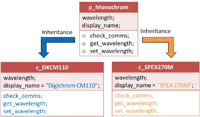
By designing parent classes for each type of equipment needed for the operation of the instrument, a strict set of properties and abstract methods is assigned to all devices of that type. While the specific operation of the device may be different, the same set of properties and methods are used to interface with them, making them virtually interchangeable. This layout is demonstrated with an abbreviated Monochromator class diagram in Figure 6.
Figure 6: Inheritance relationship for the monochromator equipment type object. The p_Monochrom parent class defines the functions that are required of the child classes, while the child classes dictate how a particular instrument executes the commands.
16
SPEX 270M actually perform these actions are drastically different, but the user will use the exact same function regardless. If an experiment is designed around one type of monochromator, any other valid monochromator object can easily replace it. Due to the shared set of methods and properties defined in the parent class, no changes to the programming would be necessary.
2.2.3. Software Class Layout
The software consists of six main categories of objects: framework, equipment, equipment component, experiment, experiment component, and data objects. The general software layout is shown in Figure 7.
17 2.2.3.1. Framework Object
The framework object is the organizational backbone for the entire software platform. On startup, it initializes and stores all of the equipment and equipment component objects available to the experimenter. Because the equipment objects need to be accessed by multiple experiments, having them in a single location provides an easy way for experiment classes to reference them.
By passing a copy of the framework into an experiment object, all of the available equipment is also passed into it. The framework class definition is shown in Figure 8.
18
All equipment objects of the same type are stored in a cell array in the appropriate object property. There are currently four properties for storing equipment in the framework object: Monochromator, DAQ, Stage, and Camera. The Camera equipment type is under development, and thus is currently empty. Referencing equipment in the framework object is done in the same manner as referencing an object property in Matlab. For example, if the framework object is named “frame”, the first monochromator loaded by the framework would be located at: frame.Monochromator{1}.
The initial equipment setup is handled by the framework object by passing it a configuration file. This simplifies the day to day initialization of the system because the equipment available to the user will likely remain unchanged for long periods of time. However, the initialization can be changed easily as needed, or customized for different table configurations. While the software was written with this microscope in mind, it will eventually replace all the instrument control software in the lab, and be used to control any future instruments. The software has been adapted for use on 3 different optical tables in lab, each of which requires a unique configuration file.
2.2.3.2. Equipment and Equipment Component Objects
Equipment objects control the physical components that make up the microscope.
This includes monochromators, motion controllers, and data acquisition (DAQ) cards. Their properties consist of useful parameters that are commonly associated with the type of equipment they represent. Because they represent physical entities, all equipment and equipment component objects are handle objects.
19
serial port, Ethernet port, or dynamic linked library (dll). There are currently 3 types of equipment classes: Monochromator, DAQ, and Stage. The Camera equipment class is currently under development.
Equipment Component objects are objects that represent the controllable sub-units
of equipment objects. In the case of the Stage and DAQ classes, there are multiple channels that may need to be addressed separately for use in experiments. In these cases, the equipment object handles any communication and data interpretation, while the user directly addresses the equipment component objects.
20
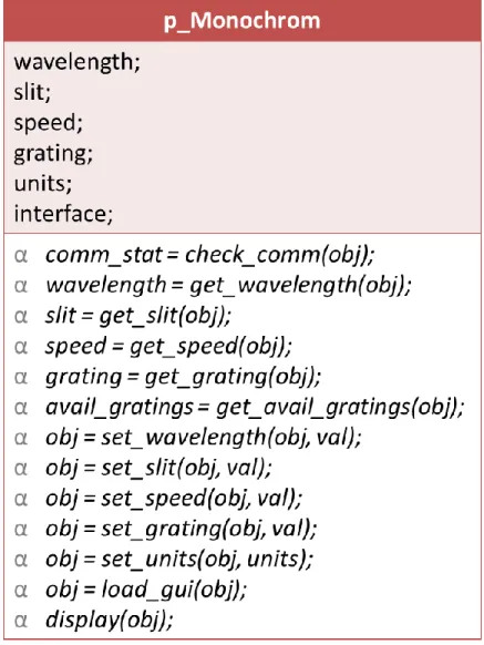
Monochromator equipment objects refer to all of the available devices for spectral
control. These are typically monochromators, but the c_Filter child class allows for the user to manually enter the wavelength for reference by other classes and methods. The Monochromator parent class, p_Monochrom, is shown in Figure 9. The description and available monochromator child classes are summarized in Table 1.
21
22
DAQ equipment objects refer to data acquisition objects such as analog to digital
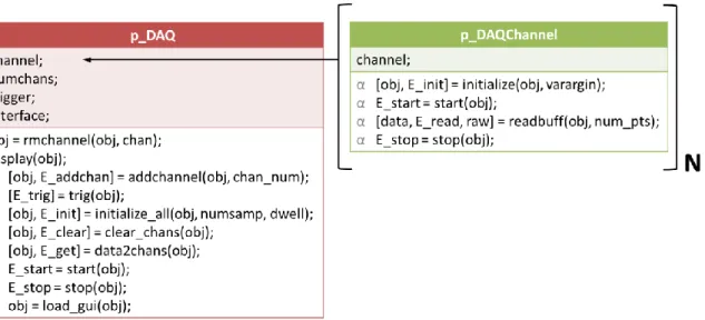
converters, counter cards, multi-channel analyzers, etc. Devices that control data collection and transfer into the computer are DAQ objects. The class diagram for the DAQ parent class, p_DAQ, is shown in Figure 10. The description and available DAQ child classes are summarized in Table 2.
Figure 10: Class layout for the DAQ and Channel objects. Channel objects are housed inside of the DAQ object in the channel property.
Channel equipment component objects refer to the individually addressable inputs
and outputs in a data acquisition card. Channel classes can be configured to function as analog input and output, digital input and output, counting. Some DAQ objects can contain various combinations of different kinds of Channels. All of the Channel objects are stored in the channel property of their corresponding DAQ object in an array of variable length represented in Figure 10. The available Channel child classes are listed in Table 3.
23
This way, unused channels on the DAQ card are still valid Channel objects, but merely non-functioning ones.
24
Table 3: Channel class summary.
Stage equipment objects refer to motion controller objects, typically single or multi
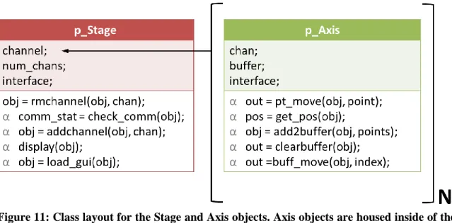
axis motion stages. In the microscope, these classes control translation of the sample, the beam, objectives, delay lines, etc. The class diagram for the Stage parent class, p_Stage, is shown in Figure 11. The description and Stage child classes are shown in Table 4.
Axis objects are the equipment component objects which address the individual
25
different objects. As with the DAQ objects, all of the Axis objects are stored in the channel property of their corresponding Stage as an array of variable length represented in Figure 11. The available Axis child classes are listed in Table 5.
Figure 11: Class layout for the Stage and Axis objects. Axis objects are housed inside of the Stage object in the channel property.
26
27
28 2.2.3.3. Data Objects
Data objects are non-physical components that are necessary for the operation of the experiment classes. They are responsible for organizing, analyzing, displaying, and saving data. By defining them as classes, they are grouped with useful properties and the methods that perform operations on them. Actions such as displaying and saving can be customized to include useful information such as scale bars or time stamps.
Figure 12: Data types in the IMP software. Depending on the experiment to be conducted the data complexity can continue to grow in the future, which the software would support.
The standard layout of data storage in IMP is shown in Figure 12. Data collected on the microscope is typically presented in either 1-D in the form of plots, or 2-D in the form of images. To cover these forms, two classes have been designed: c_Figure and c_Image. As transient data is becoming more prevalent, a new data type of c_ImageStack is being developed which will handle 3-D data consisting of stacks of multiple images or movies.
29
and collecting. The class structures for the c_Figure and c_Image classes are shown in Figure 13. The descriptions of the c_Figure and c_Image classes are shown in Table 6.
There is an inheritance relationship between c_Figure and c_Image classes, in that c_Image classes inherit all of the properties and methods of c_Figure classes. However, this relationship exists because a c_Image class is essentially a c_Figure class, but with added properties and methods. This means that the c_Image class also contains all of the properties and methods of the c_Figure class. To save space, they have been left off the class diagram for the c_Image class.
30
31 2.2.3.4. Experiment Component Objects
The last set of objects needed for running experiments with the software are the experiment component objects. These are miscellaneous objects that aid in the experimental design, but do not fit into the other categories. They do not have parent classes and their existence enables extra features in experiment objects. As of now, there are only two experiment component objects: c_Buffer and c_Mask. The class structures for the c_Buffer and c_Mask classes are shown in Figure 14, and their descriptions are shown in Table 7 and Table 8, respectively.
32
The c_Buffer object takes in an array of axis position values, translates them into “move” commands to be sent to an Axis object interface, and stores them in the commStrArray property. This is done on the fly in the Axis object’s pt_move method, but there is typically an associated overhead in building the command (e.g. checksum calculation). This overhead may be small for a single point, but imaging experiments involve doing this hundreds of thousands of times. Buffer classes eliminate this overhead by storing pre-translated move commands for each possible position. These commands are accessed by the buff_move command in the Axis class definition by imputing the index value of the pre-translated command. Each Axis object contains a c_Buffer object in its buffer property, whether or not it is actually used.
33
The c_Mask object is an object that modifies the c_Image class for use in image collection. The mask object contains a Boolean array which defines which points on an image should or should not be collected. This greatly reduces image collection time, while keeping the important parts of the image intact. The define_mask command in the Image object is used to draw rectangular or polygonal shapes to define areas to be included.
34 2.2.4. Experiment Objects
Experiment objects are the central elements of the software that execute a specific experimental procedure. The purpose of all the aforementioned objects are pieces that come together to make the Experiment objects work. As such, Experiment objects are complex objects which contain and control the other objects in order to perform the desired experiment. These are the objects that a typical experiment designer will have to create if a satisfactory one does not exist.
Like the Framework object, Experiment objects read a configuration file on initial setup. This file contains default values for the properties as well as which equipment objects will be used to conduct the experiment. This way multiple experimental setups can be stored and readily accessible.
35
Experiment classes are each very unique, containing drastically different arrays of equipment, data, and support objects. However, experiment objects inherit from a parent class, p_Experiment, which defines methods that should be available for all experiments. The class diagram for the Experiment parent class is shown in Figure 15, and a detailed description is in Table 9.
36 2.2.4.1. Methods for Experiment Class Design
When designing Experiment classes, there are three useful methods that are currently written in the p_Experiment class: collect_point, collect_line, and collect_scan_line. These are prewritten methods for data collection that are the basic ways of collecting and processing data. As the software develops further, future experiments may require the development of other methods within the parent experiment class; however, these existing methods are the building blocks for all experiments thus far.
2.2.4.2. The Collect_Point and Collect_Line Methods
The collect_point and collect_line methods in the Experiment classes are buffered data acquisition methods. This means that they use triggers to dictate the beginning and ending of data collection associated with a single point. One trigger signals the beginning of data collection, the program collects for a specific dwell time, and a second trigger signals the end.
The raw data and triggers is then sent to each DAQ Channel object and processed with the read_buff command. In the case of counters (c_GtdCtrChannel objects), the data is read directly from the buffer and the difference in counts gives the number of counts between triggers. In the case of analog inputs (c_AlgInChannel objects), the data between the triggers is averaged and the returned data is the result. These two methods are illustrated in Figure 16.
37
single-point acquisition, or multiple times, for line acquisition. The difference between successive counts represents the magnitude of the acquired signal for that point.
Figure 16: Data processing procedure for a DAQ Channel object configured for counting (TOP) and configured for continuous analog acquisition (BOTTOM). The procedure shown is the same for collect_point and collect_line methods, differing only by the number of points collected.
38
the first and second trigger is averaged to produce the collected value at that point. As with the counter, this can be done once to produce a single point or multiple times for a line.
The difference between the collect_point method and the collect_line method is automation of the motion axis. The collect_point method only requires the experiment class and a dwell time for inputs. It records a single data acquisition point for the specified dwell time and returns the result; a single data point. The collect_line method moves the specified Axis to each buffered index point provided, records for the specified dwell time, and returns the result; an array of data points. The collect_line method is used for raster scanning for imaging and reduces the overhead of processing each point before moving to the next one.
2.2.4.3. The Collect_Scan_Line Method
39
Figure 17: Data processing procedure for the collect_line_scan method. This is a continuous analog data acquisition method, which registers the coordinates of the data after collection has completed.
2.2.4.4. Single-Axis Scanning Experiment
40
into their properties. Monochromator, DAQ, and Stage classes are filled with the appropriate equipment objects to be used by the experiment. The axis1 property must contain the Axis object that will be scanned and the channel property must contain the DAQ Channel objects that will be used to collect the data. For each Channel object, a c_Figure object is created in the figure property.
Figure 18: Diagram showing the layout of the most commonly used experiment classes. Also shown are the objects contained in the properties of the experiment classes. The symbols are defined in the legend on the left side.
41
at which to collect, and the wavelength property contains the wavelength that each Monochromator object should be set to. The class diagram for the c_1AxisScan_Exp is shown in Figure 18.
2.2.4.5. Two-Axis Imaging Experiment
For two-dimensional scanning involving two Axis objects, the c_2AxisImage_Exp class is used; the class diagram is shown in Figure 18. This Experiment object configuration file defines the Monochromator, DAQ, and Stage object to be used, as well as which DAQ Channel objects to use. In this object, axis1 and axis2 need to be defined as the two Axis objects to scan. The object in axis1 will be used as the x-axis in the image, and axis2 will be the y-axis (unless the image is rotated by the rot property).
For each Channel object defined in the configuration file, there will be an Image object created in the property image, and a Mask object will be created and stored in the mask property. The properties: axis1_coords, axis2_coords, pixel_size, rot, xaxis_inv, and yaxis_inv are defined in the configuration file and the Image and Mask objects are created based on their specifications. The properties: lowerleft, upperright, center, height, and width are calculated from these values as well. The remaining properties of wavelength and dwell (in milliseconds) are set by the user, though an initial value is present in the configuration file.
There are five extra methods available to the user for the 2-Axis Imaging Experiment: setup, clear_data, mask_image, goto_coords, and display_images.
2.2.4.6. Monochromator Scanning Experiment
42
defines the Monochromator, and DAQ object to be used, as well as which DAQ Channel objects to use. For each Channel object in the channel property a c_Figure object is created in the figure property.
43
CHAPTER 3. HYBRID STANDING WAVE AND WHISPERING GALLERY
MODES IN NEEDLE-SHAPED ZnO RODS: SIMULATION OF EMISSION MICROSCOPY IMAGES USING FINITE DIFFERENCE FREQUENCY
DOMAIN METHODS WITH A FOCUSED GAUSSIAN SOURCE
[Reproduced from The Journal of Physical Chemistry C, 117(20), 2013, 10653-60]
3.1. Abstract
Two-photon emission microscopy is used to investigate the photoluminescence properties of individual ZnO rods. The rods are 10-20 μm in length with a tapered cross section that varies from 1-2 μm at the midpoint to several hundred nanometers at the ends. The tapered shape and hexagonal cross section result in complex optical resonator modes that lead to periodic patterns in the two-photon emission image. Finite-difference frequency domain methods using a series of excitation sources, including focused Gaussian, point dipole and plane wave, suggest that resonator modes have both standing wave (Fabry-Pérot) and whispering gallery mode character, whose relative contributions vary along the rod axis.
3.2. Background
44
ZnO nanorods, which have been described by several groups(9-11). The size of the resonator determines the optical frequencies that are supported, which are often observed spectroscopically as a series of narrow resonances superimposed on the broader band-edge and trap emission bands(12-19).
While longitudinal modes are clearly important to our understanding of the light-matter interactions of these structures, this work focuses on the cavity-modes supported within the hexagonal cross-section and lie transverse to the rod axis. The faceted crystalline structures of these ZnO materials give rise to a rich variety of optical cavity modes. Previous reports describe these modes using two classic resonator pictures: Fabry-Pérot (FP) modes supported between two opposing parallel facets, and whispering gallery (WG) modes arising from the circulation of light around the periphery of rod through total internal reflection at each crystal face(13, 15-22).
45
modes actually contain characteristics of both the FP and WG resonances, whose relative contributions vary with resonator size. At smaller sizes, the modes have primarily standing-wave character with much of the optical intensity located in the core of the structure. As the size is increased, the intensity distribution shifts to the periphery of the structure, becoming more WG-like in character. These two different mode types may explain the spatial variation in electron-hole recombination that are observed these structures. Pump-probe microscopy experiments from our lab(25, 26) indicate that recombination in the tips of the rod proceeds through an electron-hole plasma state, suggesting that carriers are created in a bulk-like region of the rod, i.e. the core. In the larger sections of the rod, electron-hole recombination is trap mediated, consistent with carriers being produced in the depletion zone near the surface and undergoing rapid charge separation.
3.3. Experimental
ZnO rods were grown using hydrothermal methods adapted from previously published work(29, 30). An aqueous solution of Zn(NO3)2 (50 mM) and
hexamethylenetetramine ((CH2)6N4) (50 mM) was heated in a closed bomb to yield
46
to perform both optical and electron microscopy on the same structure allows photophysical observations to be correlated with detailed structural information.
Two-photon emission imaging was accomplished by combining an ultrafast laser source with a home-built far-field optical microscope (Figure 19A). The femtosecond laser source consisted of a mode-locked Ti:Sapphire laser (730 nm, 80 fs, 80 MHz) pumped by a solid-state diode-pumped Nd:YVO4 laser. The laser output was directed
onto the back aperture of a 50x microscope objective (0.8 NA), which focused it to a diffraction limited spot, resulting in two-photon excitation at a localized region of the ZnO rod. Light emanating from the structure was collected by the objective, passed through a dichroic beam-splitter, and focused onto the slit of a monochromator and photomultiplier tube (PMT). Emission images were collected by raster scanning the sample across the focal point of the objective with a piezoelectric nano-positioning stage while monitoring the intensity of the emitted light. Imaging was performed without a coverslip under ambient conditions.
47
Figure 19: (A) Diagram of the two-photon emission microscope. The 730 nm output of a mode-locked Ti:Sapphire laser is directed onto the back aperture of the microscope objective (50x, 0.8 NA) and focused to a diffraction-limited spot at the sample. Imaging is achieved by raster scanning the sample stage across the focused laser spot and monitoring the emission collected by the objective with a scanning monochromator/PMT. (B) Two-photon emission image of a 100 nm quantum dot with 810 nm excitation. The size of the emission feature suggests that the lateral resolution at this wavelength is approximately 410nm.
3.4. Results And Discussion
Figure 20: (A) SEM image and (B) emission spectrum of a tapered zinc oxide nanorod. The red circle and double-headed arrow indicate the location at which the spectrum was acquired and the direction of the excitation polarization vector, respectively. (C-D) Photoluminescence images taken at 390 nm and 550 nm, respectively, show a modulated emission pattern along the structure. The lower case letters in (C) indicate the resonance spots discussed in the text.
49
An individual structure is excited by a focused near infrared laser pulse polarized parallel to the long-axis of the rod, resulting in a two-photon absorption that promotes carriers from the valence band to the conduction band in a localized region of the structure. Because ZnO is transparent in the near infrared, two-photon absorption will occur throughout the excitation volume. Single UV photon absorption at 365 nm, by comparison, would occur within 100 nm of the surface. Free carriers produced by photoexcitation will either relax into excitons, resulting in the intense near-UV emission, or become trapped in defect sites, giving rise to the broad visible emission (Figure 20B).
Emission imaging is achieved by monitoring the photoluminescence intensity at a particular wavelength as a function of two-photon excitation position. Previous work in our lab showed that the majority of the emission detected emanates from the location of laser excitation, indicating that while coupling of light (either the excitation or emission) into wave-guiding modes propagating along the long axis of the rod does occur, it is relatively weak and contributes little to the observed emission at a given point(27). A striking feature of images compiled from either band edge emission (em = 390 nm) or
trap emission (em = 560 nm) is the axially symmetric intensity modulation along the
50
tapered structure, the cavity size changes along the long axis of the rod, causing the excitation wavelength to go in and out of resonance as the focused laser spot is moved along the rod. While in principle either the excitation or the emission wavelength could be resonant with the cavity, the qualitative similarity between the two images suggests that the excitation wavelength is largely responsible for the observed patterns.
3.5. Standing-Wave and Whispering Gallery Mode Descriptions
Generally, there are two types of optical modes: standing wave (Fabry-Perot, FP) resonances that are supported between two parallel facets, and whispering gallery (WG) modes that correspond to propagation of light around the periphery of the hexagonal cross-section through total internal reflection off each facet. Both are characterized by resonance conditions that depend upon the resonator size and wavelength, i.e.
1 2
2
6
tan 3 4
3 m FP m WG d m n
d m n
n
(1a) (1b)
where m FP
d and dWGm are the facet separations for the mth mode in the FP and WG resonances, respectively, is the wavelength and n is the index of refraction. The value of β is based on the polarization of the excitation source, being β = n for TM (Ec) and β = n-1 for TE (Ec).
The distance between resonance spots in the emission images, ΔL, depends upon the taper angle of the structure, with smaller cone angles giving rise to larger separations, i.e.
51 where Δd is the mode spacing, i.e. (dm+1
-dm ), and α is the change in facet spacing per unit
length along the structure.
Figure 21: (A) Facet spacing determined from the SEM image in Figure 20A plotted as a function of position along the rod. (B) Intensity profiles obtained by integrating a column of pixels at each longitudinal position along the images for both the band-edge and trap emission images (Figure 20C and Figure 20D). The calculated whispering gallery mode locations for 730 nm and 390 nm light are indicted by the two brackets positioned between (A) and (B). The lower-case letters in the band-edge profile correspond to the resonance spots indicated in Figure 20B.
52
3 / 2
d w, and is depicted as a function of position along the rod in Figure 21A. The α-values extracted from the slopes on the right and left side are 101 nm/µm and 103 nm/µm, respectively, indicating that the rod is nearly symmetric with a consistent taper throughout the much of the structure.
The predicted spacing between resonance spots along the rod are ΔLFP=/2nα and
ΔLWG=/3nα for the two different optical mode types. Using an average α-value of 102
nm/µm, and n=2 for the index of refraction of ZnO at 730 nm(32) leads to predicted separations of ΔLFP = 1.8 μm and ΔLWG =1.2 μm.
Intensity profiles along the long axis for the band-edge and trap emission images (Figure 21B) show the resonances to be nearly equally spaced with an average ΔL of 1.0-1.2 μm. This spacing is qualitatively consistent with the WG mode description and significantly smaller than the spacing predicted by the FP resonance condition. The locations of the WG resonances for the first five modes (=730 nm), indicated by the bracket placed above the emission profile, coincide with the locations of the emission maxima.
53
mode (see 390 nm bracket, Figure 21). Amplified spontaneous emission, and even lasing, of the band-edge photoluminescence has been observed in ZnO nanostructures. While we do not observe evidence of actual lasing, previous work in our lab(23) showed that the band-edge emission has a greater than quadratic power dependence on pulse intensity. This is particularly true when the rod is excited at one of the resonance spots,(23) suggesting that the emission is likely reinforced by the cavity modes as the 390 nm emitted light is reflected off the facets and returns to the excitation region. The trap emission, on the other hand, shows simple quadratic dependence. The larger scaling factor for the band-edge emission effectively results in a higher spatial resolution, accounting for the greater contrast difference between the band-edge and trap emission images.
These WG mode description qualitatively account for many of the features observed in the emission images, but it does not explain, the existence of the spots at the ends of the rod (denoted a and a'). At this point d = 160 nm. This is far below the 450 nm predicted by the WG resonance condition (Eqn 1b) for the m=1 resonance with λ=730 nm, and also smaller than the 210 nm spacing obtained with λ=390 nm. Interestingly, it is close to the spacing calculated using the FP resonance condition (Eqn 1a) for the m=1 mode at 730 nm, underscoring the idea that neither picture adequately describes the resonance properties of these structures.
3.5.1. Finite Difference Frequency Domain (FDFD) Simulations
54
series of two-dimensional calculations. The 2D model of each individual resonator (see Figure 22A, for example) consists of a square box (air) with a hexagonal slab (ZnO) placed at the center. The box is surrounded by a perfectly matched layer (PML) that eliminates electromagnetic reflections at simulation boundaries. The mesh spacing used in the simulations, defined as the size of the largest cell, was 30 nm, which is approximately 10 times smaller than the wavelength inside the ZnO material. Simulations performed with a smaller mesh size (15nm) yielded identical results, confirming the appropriateness of this choice. FDFD methods, which were implemented using the COMSOL Multiphysics software package (version 4.3), solve for the electromagnetic field in response to a single-frequency source, resulting in a steady-state map of the optical intensity distribution inside the resonator. We have examined four different sources: (i) point-source, (ii) line source, (iii) focused Gaussian beam, and (iv) plane-wave. The first two provide a crude approximation of the localized laser excitation; the third is realistic representation of the focused laser beam used in the experiment, while the last provides a comparison with far-field excitation configurations. In each case, the source is polarized with the electric field perpendicular to the simulation plane and the output of the simulation is the EM field inside the simulation area.
(i) Point Source: The simplest localized excitation scheme is an oscillating ( = 411
THz, = 730 nm) current density point source positioned 25 nm above the center of the topmost facet. Figure 22B shows the average optical intensity inside the resonator (i.e.
55
Figure 22: (A) Diagram of the simulation environment depicting the point source configuration. The line source (not shown) is placed in the same location and is 440 nm wide. (B) Plot of the average intensity (〈 〉 ∫| | ) as a function of the facet spacing (d) for both the point source (black) and line source (red). (C-J) Spatial intensity maps | | for resonators with facet spacing d = 370 nm, 630 nm, 760 nm and 1020 nm for the point source (C-F) and line source (G-J). Blue corresponds to zero intensity, red is max intensity.
56
reflection at each facet minimizes loss, resulting in multiple round trips and narrow resonances. The broadening of the resonances as the cavity size decreases suggests an increased loss per round trip. This most likely occurs at the vertices, which become a dominant feature at the smaller sizes.
The spacing between modes is not constant across this size range. The Δd spacing between the sharp peaks at larger cavity size is 130 nm, similar to that predicted by the WG mode resonance condition (Eq 1b). Interestingly, for the broader resonances, at smaller cavity sizes, Δd is about 160 nm, which matches the FP spacing (Eq. 1a) Although the presence of standing-wave character is not obvious from the mode patterns, the EM sources described below suggest that the modes best described as hybrid resonance with both WG and FP character.
(ii) Line Source: While the point source is qualitatively appealing, it is not a good
representation of the experimental configuration, where the spatial extent of excitation is several hundred nanometers. A similar calculation in which the point source is replaced by a line 400 nm long and centered at 25 nm above the top facet addresses this shortcoming. The results from this simulation, which are shown alongside those for the point source in Figure 22, highlight the role that the source plays in shaping the field patterns.
57
increase in the intensity present in the center of the resonator. While the results for the larger diameter are unaffected by the change in source, there are significant differences at smaller sizes (d < 600 nm). First, the broad resonances at smaller diameters have drastically higher average intensities in the line source model than the point source (Figure 22B). Moreover, the field distributions are also affected. Whereas the point source produces a mode pattern in the 370 nm resonator that is largely WG in nature, the patterns obtained with the line source takes on more standing-wave character (Figure 22G). As the cavity size increases (630 nm and 760 nm), the modes are neither completely WG nor FP like in character (Figure 22H-I), but rather a combination of the two. The simulations point to the presence of two modes progressions, where at large cavity sizes the resonances are dominated by WG modes, and at small cavity sizes they are dominated by FP character. Hybrid resonances that contain elements of both are observed where the two progressions overlap, which appears to occur when the source and top facet are of similar sizes. These results underscore the need for adequately modeling the EM source in simulating the emission patterns of these structures.
(iii) Gaussian Source: An optical source that mimics the focused Gaussian beam used
in the experiment is implemented by specifying the EM field along the boundary, i.e.
( ) (3) where yB is the distance from beam waist to the boundary, x is the coordinate along the
58
Figure 23: (A) Diagram of the focused Gaussian simulation environment. The EM source is functionalized according to Eq 3 with the x and y dimensions corresponding to the horizontal and vertical axes and the origin located at the center of the simulation box. (B) Spatial map of the optical field | | produced by the Gaussian source in the absence of the resonator.
radius of the beam waist at the focus, , is defined at the 1/e width of the electric field.
The functions , , and
are the beam width, radius of curvature, and Gouy phase at the boundary,
respectively, and . With this boundary condition, the EM field focuses to a
minimum spot size at the center of the simulation box (y = 0). An intensity map of the
optical field, | | , produced by this Gaussian source, in the absence of the
hexagonal resonator, is shown in Figure 23B. With , the lateral width of the two-photon volume created by the source, obtained by examining | | , is around 420 nm, which is comparable to the lateral resolution of two-photon excitation in our microscope.