Molecular doping enabled scalable blading of
ef
fi
cient hole-transport-layer-free perovskite solar
cells
Wu-Qiang Wu
1,2, Qi Wang
1,2, Yanjun Fang
2, Yuchuan Shao
1,2, Shi Tang
2, Yehao Deng
1,2, Haidong Lu
3,
Ye Liu
2, Tao Li
3, Zhibin Yang
1, Alexei Gruverman
3& Jinsong Huang
1,2The efficiencies of perovskite solar cells (PSCs) are now reaching such consistently high levels that scalable manufacturing at low cost is becoming critical. However, this remains challenging due to the expensive hole-transporting materials usually employed, and diffi -culties associated with the scalable deposition of other functional layers. By simplifying the device architecture, hole-transport-layer-free PSCs with improved photovoltaic performance are fabricated via a scalable doctor-blading process. Molecular doping of halide perovskite
films improved the conductivity of thefilms and their electronic contact with the conductive substrate, resulting in a reduced series resistance. It facilitates the extraction of photoexcited holes from perovskite directly to the conductive substrate. The bladed hole-transport-layer-free PSCs showed a stabilized power conversion efficiency above 20.0%. This work repre-sents a significant step towards the scalable, cost-effective manufacturing of PSCs with both high performance and simple fabrication processes.
DOI: 10.1038/s41467-018-04028-8
1Department of Applied Physical Sciences, University of North Carolina, Chapel Hill, NC 27599, USA.2Department of Mechanical and Materials Engineering,
University of Nebraska–Lincoln, Lincoln, NE 68588, USA.3Department of Physics and Astronomy, University of Nebraska–Lincoln, Lincoln, NE 68588, USA.
S
ince theirfirst report in 2009, halide perovskite solar cells (PSCs) have attracted enormous interest as emerging light-to-electricity conversion optoelectronic devices with both high efficiency and ease of solution processability1–3. To date, the power conversion efficiencies (PCEs) of solution-processed PSCs have been certified at well above 20%4–6. However, all top-performing PSCs were fabricated by a spin-coating method which is unsuitable for high throughput and scalable module produc-tion. Several scalable film deposition techniques have been developed for PSC fabrication, such as doctor-blading7–10, spray deposition11, slot-die coating12, solution printing13, and electro-deposition14. In particular, doctor-blade coating with a controlled substrate temperature has gained most success in depositing high-quality perovskite films with large grains and controllable optoelectronic properties15. Moreover, blade coating has great potential to be scaled up for roll-to-roll fabrication. Encoura-gingly, the PCEs of PSCs with bladed perovskite layers have steadily increased to above 19%, approaching the levels of their spin-coated counterparts13,16.A next step towards the scalable fabrication of PSCs is to coat the charge transport layers by scalable processes. However, the existing multiple-layer device structures, either p–i–n or n–i–p structures with a hole transport layer (HTL), perovskite, and electron transport layer (ETL), impose a great challenge on the scalable fabrication of PSCs in a cost-effective manner17–20. First, high-performance organic hole-transporting materials, such as 2,2′,7,7′ -Tetrakis[N,N-di(4-methoxyphenyl)amino]-9,9′-spirobifluorene (spiro-OMeTAD), are much more expen-sive than perovskite materials. Second, for the devices with p–i–n structure, it is difficult to blade-coat perovskitefilms onto a hydrophobic HTL, e.g., poly(bis(4-phenyl)(2,4,6-trimethyl-phenyl)amine) (PTAA), while a hydrophilic HTL, e.g., NiOx, is difficult to form on plastic substrates at low temperature, nor can easily be coated at optimal thickness and electronic quality to achieve the highest device efficiency. Hence, we believe that the elimination of the HTL from the PSC device architecture can be an effective way to solve this challenge. By reducing one step of the standard coating process, at least one third of the manufacture cost and time can be saved, in addition to savings of material cost for the HTL.
The reported ambipolar charge transport characteristics of halide perovskite materials endow them with great potential to construct PSCs with simplified device architecture, such as HTL-free PSCs with either conventional or inverted structure21–23. Yet, a critical challenge for HTL-free PSCs is the ineffective hole collection by indium tin oxide (ITO) because of mismatched work functions between ITO and the perovskite, which generally causes significant efficiency loss23–25. In addition, the construc-tion of HTL-free devices by the blade-coating method faces more challenges due to rougher and more non-uniform perovskite
films, than do those prepared by spin-coating with the anti-solvent method.
Here we report a molecular-doping strategy for a perovskite layer to doctor-blade HTL-free PSCs with a simplified device structure of ITO/perovskite/ETL/Cu. Doping methylammonium lead iodide (MAPbI3)films with 2,3,5,6-tetrafl uoro-7,7,8,8-tetra-cyanoquinodimethane (F4TCNQ), a strong electron-withdrawing molecule, leads to a modified ITO/MAPbI3 interface with favorable band bending, which facilitates the extraction of pho-toexcited holes from perovskite to ITO electrode. Combining additive engineering and solvent annealing, high-quality MAPbI3
films are obtained with full surface coverage, micrometer-sized grains, and improved crystallinity. By employing a bladed and doped MAPbI3film as the photoactive layer in a HTL-free device structure, a stabilized PCE over 20.0% with almost no J–V hys-teresis is obtained.
Results
Perovskite films fabrication and molecular doping. The MAPbI3perovskitefilms were directly deposited onto blank ITO glass substrates by a previously reported doctor-blading method9, which is schematically illustrated in Fig.1a. Before blade coating, the ITO substrates were cleaned by a UV-ozone treatment to improve their wettability to perovskite solution23. MAPbI3 pre-cursor dissolved in N,N-diethylformamide (DMF) containing p-type dopant (F4TCNQ) was dripped onto substrates which were heated at 150 °C, followed by a quick blading process to spread the solution onto the substrates. After blading, the perovskite precursor solution dried in a few seconds, and the substrates were quickly removed from the hot plate and annealed at 100 °C for varied durations. The bladed perovskitefilms showed thicknesses of 500 ± 20 nm from cross-sectional imaging (Fig. 1b) by scan-ning electron microscopy (SEM). To implement molecular dop-ing of the perovskite layer, F4TCNQ with chemical structure shown in Fig. 1a was dissolved in DMF separately, and then added to the as-prepared MAPbI3precursor solution. Perovskite
films made without or with F4TCNQ were denoted as MAPbI3or MAPbI3:F4TCNQ, respectively.
The doping of perovskite is expected to change the work function of thefilms. Kelvin probe force microscopy (KPFM) was used to determine the surface potential change of perovskitefilms upon F4TCNQ mixing. In addition to direct mixing of F4TCNQ and MAPbI3 in precursor solution, MAPbI3:F4TCNQ was prepared by solid diffusion via heating F4TCNQ powder on MAPbI3and then removing the excess F4TCNQ. The topography and contact potential difference (CPD) images of pristine MAPbI3and MAPbI3:F4TCNQfilms by either standard solution mixing or solid diffusion are shown in Fig. 1c–h. For better comparison, the three CPD images areflattened and presented in the same color scale, while the histograms of the absolute CPD values of the three types offilms are plotted in Fig.1i. The pure MAPbI3 film has coarse grains and uniform CPD distribution (Fig.1c, f). In contrast, solution mixed MAPbI3:F4TCNQfilm, in which uniform doping is expected, has fine grains and greater heterogeneity of the CPD distribution (Fig.1d, g). For the sample with solid-diffused F4TCNQ, some small F4TCNQ particles were placed on top of a MAPbI3 film, and the CPD imaging was conducted around the edge (the green color line as indicated in Fig.1h) to include both neat and doped perovskite regions. Such method leads to a clear edge between diffused and undiffused regions that can be visualized in the CPD image (Fig. 1h), thus the CPD heterogeneity is even higher. The change of absolute CPD caused by F4TCNQ doping is clearly demonstrated in Fig. 1i. A decrease of surface potential or in other words an increase of work function was observed for the MAPbI3:F4TCNQ
strategy enabled the fabrication of an HTL-free PSC with a simplified device configuration but still effective p–n heterojunc-tion (i.e., p-doped perovskite and n-type ETL), and thus enhanced device performance.
Electronic properties of doped perovskitefilms. The electronic properties of the MAPbI3:F4TCNQ films were investigated by comparing their current density–voltage (J–V) characteristics with pristine MAPbI3 films deposited on glass substrates in the dark condition. The lateral conductivity was measured across gold electrodes spaced 100 µm apart (Fig. 2a). As shown in Fig. 2b, the MAPbI3:F4TCNQ film exhibited a nearly tenfold increase in conductivity over the neat MAPbI3film, which
con-firmed that F4TCNQ doped MAPbI3. The charge transfer from MAPbI3 to F4TCNQ is expected to cause quenching of photo-luminescence (PL) from the MAPbI3layer, which was measured by using time-resolved photoluminescence (TRPL) decay for MAPbI3 films deposited on glass substrates (Fig. 2c). The MAPbI3:F4TCNQ prepared on glass substrate showed a PL life-time of 65 ns, which is fourfold shorter than the PL lifelife-time of pristine MAPbI3film (268 ns) on glass.
The relative large molecular size of F4TCNQ likely prevents its integration into the lattice of MAPbI3. Therefore, we speculate
that F4TCNQ molecules most probably remain at the grain boundary (GB) regions of perovskite films and/or perovskite/ electrode interfaces. To determine the lateral distribution of F4TCNQ molecules, the local dark conductivity at grains and GBs was measured using conducting atomic force microscopy (c-AFM). Figure 2d illustrates the c-AFM setup, where the microscope tip was positioned at locations randomly chosen from topographic AFM images (Fig. 2e, g). The tip bias was scanned in the range+2.0 to−2.0 V at a rate of 0.14 V s−1. For the neat MAPbI3film, the dark currents were similar at the grain and GB regions (Fig.2f and Supplementary Fig.2a, b), which is in accordance with previous reporting28. In sharp contrast, the dark currents measured at the GB regions of the MAPbI3:F4TCNQ
film were notably higher (Fig.2h and Supplementary Figs.2c, d), elucidating the remarkably improved conductivity at the GB region after molecular doping of MAPbI3 by F4TCNQ. At the regions close to GBs, the F4TCNQ molecules and MAPbI3 undergo charge transfer, leading to an increase in carrier density in MAPbI3and thus the enhanced dark conductivity29.
Morphologies and crystallinities of perovskite films. High-quality perovskite films with large grains, high crystallinity and complete surface coverage are also crucial to achieving
high-Perovskite film
Perovskite ink ITO
Blade a
F4TCNQ
500 nm b
F F
F F
N N
N N
2 2 μm d
nm 200
0.00
–200
Height
c
nm 200
0.00
–200 2
2 μm 2 2 μm
e
nm 200
0.00
–200 10 10 μm
CPD
f g
MAPbI
3
–4.0
–5.5 –5.2
–8.3
F4TCNQ
j
Number of points
i
MAPbI3
F4TCNQ solid-diffused MAPbI3 F4TCNQ-doped MAPbI3
Potential (V)
mV 40.0
0.00
–40.0
3000
2500
2000
1500
1000
500
0
–0.10 –0.05 0.00 0.05
mV 40.0
0.00
–40.0
h
Diffused region
mV 40.0
0.00
–40.0
10 10 μm 2
2 μm 2 2 μm
Fig. 1Doctor blading and doping of perovskitefilms by F4TCNQ.aSchematic illustration of a doctor-bladed perovskitefilm and the chemical structure of F4TCNQ dopant.bCross-sectional SEM image of the MAPbI3film deposited directly onto ITO glass via bladed coating at 150 °C, showing thefilm thickness of around 500 nm. Topography KPFM images ofc,fMAPbI3,d,gF4TCNQ-doped MAPbI3, ande,hF4TCNQ solid-diffused MAPbI3films. CPD represents the contact potential difference between the tip and sample’s surface.iSurface potential profiles of different perovskitefilms as indicated.j
performance HTL-free devices. The blending of F4TCNQ in the perovskite in a small percentage (ranged from 0.01 to 0.05 wt%) did not notably change the morphology and grain size of the perovskitefilms, as shown by the SEM images in Supplementary Fig.3, nor cause a drastic change of crystallinity, as shown by the XRD patterns of bladed MAPbI3 films prepared with different amounts of F4TCNQ in Supplementary Fig. 4. Accordingly, methylammonium hypophosphite (MHP) and methylammo-nium chloride (MACl) were introduced as additives to the pre-cursor solution, and co-solvents (dimethyl sulfoxide (DMSO)/ chlorobenzene (CBZ)) post-annealing process was also combined to achieve a high-quality and high-crystalline MAPbI3 film
(Supplementary Figs. 5,6and7for SEM images and XRD pat-terns of bladed MAPbI3films prepared with different amounts of MHP as well as using co-solvents annealing technique in the absence or presence of MACl)9,10,16,30,31. Figure 3a, b show representative SEM images of the bladed perovskite films after optimization, which featured a uniform morphology that exten-ded hundreds of micrometers. The perovskite domains were densely packed together, and without observable voids at domain boundaries (Fig.3a). It should be noted that these domains are not single crystalline grains. Each micrometer-scale convection domain was comprised of micro-sized grains ranging from 800 to 1700 nm (average above 1μm, Fig.3b).
100 μm a
Perovskite Glass
Au Au
800 600 Time (ns)
400 200 1E–3
0.01
Normalized PL
0.1
c
Glass/MAPbI3:F4TCNQ Glass/MAPbI3
1
0
e
Grain1
Grain3
Grain2
GB1
GB2
GB3
1 μm
g
Grain4 GB4
Grain5
Grain6
GB5
GB6
1 μm
4 2 0 –2 –4 1E–11 1E–10 1E–9 1E–8
1E–7 MAPbIMAPbI33:F4TCNQ b
Current (A)
Voltage (V)
d
Tip
A
ITO Perovskite
250
f
Grain1 GB1
200
150
Current (pA)
100
50
0
–2 –1 0
Voltage (V)
1 2
h
Grain4
GB4
Current (pA)
600
500
400
300
200
100
0
–2 –1 0
Voltage (V)
1 2
Photovoltaic performances of doped perovskite devices. The impact of molecular doping by F4TCNQ on photovoltaic per-formance was investigated in detail. As illustrated in Fig. 3c, inverted HTL-free PSCs were fabricated with a device confi g-uration of ITO/MAPbI3:F4TCNQ/ETL/Cu. The corresponding photovoltaic performances for PSCs based on different F4TCNQ concentrations have been displayed in the Supplementary Table1, which indicated the optimal F4TCNQ concentration was 0.03 wt%. Figure 3d shows the current density vs. voltage (J–V) characteristics of PSCs based on the pristine MAPbI3films and MAPbI3:F4TCNQ films (with 0.03 wt% F4TCNQ), with photo-voltaic parameters summarized in Table 1. The reference PSC without F4TCNQ (i.e., MAPbI3) exhibited a poor PCE of just 11.0%, which is in accordance with that of most reported HTL-free PSCs23,24. Surprisingly, with the addition of F4TCNQ, notable concurrent enhancements of the Jsc, Voc, and FF have been achieved. The champion cell based on MAPbI3:F4TCNQ
film achieved the highest PCE of 20.2%, with aJscof 22.7 mA cm−2, aVocof 1.10 V, and a FF of 0.81. To the best of our knowledge, this is the record efficiency for the bladed PSCs in the absence of HTLs. For comparison, the PSC based on the PTAA HTL and undoped MAPbI3 layer has been fabricated, which showcases a PCE of 19.5%, along with aJscof 22.1 mA cm−2, aVocof 1.12 V, and a FF of 0.79. This result is in good agreement with our previous reports8,9,16. It is worth noting that the demonstrated HTL-free device showed similar or even better photovoltaic performance, highlighting the effectiveness of such a doping strategy for constructing high-performance PSCs with not only a simpler structure, but also less deposition steps and lower material cost. TheJ–Vcurves of MAPbI3:F4TCNQ-based device were measured in both reverse and forward scan modes at a scan rate of 0.1 V s−1, and almost no hysteresis was observed (Sup-plementary Fig. 8). Figure 3e shows the stabilized photocurrent density of this device as measured at 0.93 V, giving a stabilized PCE exceeding 20.0% under continuous light soaking. This high stabilized PCE output is among the best record for HTL-free PSCs, and is quite remarkable given that the device is prepared using a scalable fabrication method. Figure3f shows the external quantum efficiency (EQE) of the champion device. The integrated Jsc from the EQE measurement agreed well with the Jsc values measured under AM 1.5 G one sun illumination (Fig. 3d). The fabrication procedure was repeated to confirm the reliability and reproducibility of the results. The PCE histogram was collected from 30 independent cells (Fig.3g), revealing that more than 73% of the cells had PCEs above 18.0%, and more than 93% had PCEs higher than 17.0% under one sun illumination. A study of the stability for the devices with or without HTL has been conducted.
a b
100 μm 2 μm ITO
MAPbI3:F4TCNQ ETL Cu c
d
15 10 5 0 –5 –10 –15 –20 –25
–0.2 0.0 0.2 0.4 0.6 Voltage (V)
0.8 1.0 1.2
MAPbI3 MAPbI3:F4TCNQ
Current density (mA cm
–2
)
Integrated
Jsc
(mA cm
–2)
f 25
800 700 600 Wavelength (nm)
500 400 0 20 40
EQE (%)
60 80 100
20
15
10
5
0
g e
25
20
15
PCE (%)
10
5
0 25
20
15
10
5
0
70 60 50 40 Time (s) 30 20
PCE Current density
Current density (mA cm
–2)
10
15 16 17 18
PCE (%)
19 20 21
15
10
Counts 5
0
Fig. 3Perovskitefilm morphology, device structure, and photovoltaic performance.aLow magnification andbhigh magnification SEM images of bladed and doped MAPbI3film prepared with MHP (0.225 wt%) and MACl (0.5 wt%) as additive, followed by co-solvents annealing treatment.cSchematic illustration of the HTL-free device configuration.dJ–Vcharacteristics,eSteady-state current and stabilized PCE measured at a maximum power point (0.93 V),fEQE and integrated current density, andgPCE histogram of PSCs based on MAPbI3:F4TCNQfilms (with 0.03 wt% F4TCNQ)
Table 1 Photovoltaic parameters of PSCs employing neat or doped perovskite layers under one sun light illumination (AM 1.5 G, 100 mW cm−2)
PSCs Jsc(mA cm−2) Voc(mV) η(%) Average
η(%)
FF
MAPbI3 19.7 1.00 11.0 9.52 ± 0.72 0.56 MAPbI3:
F4TCNQ
22.7 1.10 20.2 18.85 ± 0.35 0.81
The devices were stored under ambient conditions (where humidity and temperature were about 20% and 25 °C, respec-tively) without any encapsulation. As compared to the devices with HTL, the HTL-free device exhibits a slightly better stability, which maintained over 92% of its initial PCE after storage for 500 h (Supplementary Fig.9).
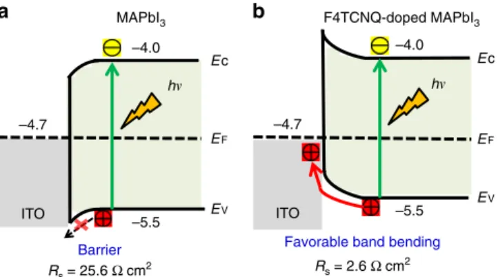
It is noted from Fig.3d and Table1that the almost twofold efficiency enhancement in the F4TCNQ-doped devices primarily originates from the remarkable FF increase. Further analysis of the J–V curves in Fig. 3d revealed that F4TCNQ doping of the perovskite layer significantly reduced device series resistance (Rs) from 25.6Ωcm2 for undoped device to 2.6Ωcm2 for doped device. The influence ofRson device FF has been well established in diode based solar cells32, according to the classical equation based on diode equation:
I¼ILI0exp
qðVþIRsÞ nkT
ð1Þ
where I is the device output current, ILis the maximum light generated current, I0 is saturated dark current, Rs is series resistance, n is ideal factor, k is Boltzmann constant, T is temperature. Assuming a diode ideal factor of 1, the FFs for the undoped and doped devices were calculated to be 53% and 83% from Eq. (1), which are very close to measured values of 56% and 81%, respectively. This indicates the increased FF for the devices with doped MAPbI3 is mainly caused by the reduction of the series resistance. To find out the origin of reduced series resistance by F4TCNQ doping, energy level diagrams are constructed and shown in Fig.4for the perovskite/ITO interface with or without F4TCNQ doping. Here the energy levels were extracted from the literature for the films made with same composition and similar method33,34. For undoped MAPbI3, the Fermi level of pristine MAPbI3(nearly intrinsic) is slightly lower than that of ITO (−4.7 eV)34. The Fermi level lines up during contact formation and causes a downward band-bending in MAPbI3, which forms a barrier for hole extraction from MAPbI3 to ITO (Fig.4a). This would also increase the possibility of charge recombination and increase series resistance at the ITO/ perovskite interface. In contrast, the incorporation of F4TCNQ in the MAPbI3 films turns the MAPbI3 to more p-type, particularly at the interface of ITO and MAPbI3, which should avert band-bending direction (Fig. 4b). This was confirmed by surface potential measurement that the F4TCNQ doping can increase work function of perovskite by ~0.1 to 0.2 eV (Fig. 1i). As is shown in Fig. 4b, the F4TCNQ doping results in an upward band bending at the ITO/MAPbI3:F4TCNQ interface. In this case, the hole transfer from F4TCNQ-doped MAPbI3to
ITO is thus facilitated, resulting in a reduced series resistance to increase FF35.
The diode Eq. (1) predicts thatRsvariation has no influence on device Voc, while in our case, the F4TCNQ doping increased device Vocfrom 1.00 to 1.10 V. This discrepancy indicates there is another factor, in addition to Rs, which leads to the Voc enhancement. To find out the reason, a transient photovoltage spectroscopy (TPV) measurement was also carried out to understand the charge carrier recombination dynamics. As shown in Supplementary Fig. 10, the MAPbI3:F4TCNQ-based PSC had a longer carrier lifetime (0.69μs) than the reference device based on neat MAPbI3(0.30μs) under one sun illumina-tion. This result was consistent with the largerVocfor the device with doping. The observed carrier recombination lifetime enhancement could be a result of band-bending configuration change due to doping, though there may be other reasons that may also change the carrier recombination lifetime. For instance, for the device with undoped MAPbI3, the retarded hole extraction would increase the possibility of charge recombination, because they cannot be effectively extracted out.
Discussion
We demonstrated how molecular doping influences the series resistance and interfacial charge transfer within HTL-free PSC devices with or without F4TCNQ incorporated in the perovskite layer. In the absence of HTL, both the electrons and holes can transport to the ITO/perovskite interface and recombine there, leading to serious interfacial charge recombination and thus inferior charge collection36. In addition, the mismatched work functions between perovskite and ITO would induce an unde-sirable energy barrier that leads to inferior hole transfer. These situations are all very detrimental to device performance. Mole-cular doping of perovskite by F4TCNQ to some extent induces favorable interfacial band bending, which allows efficient trans-port of holes at ITO/perovskite interface (Fig. 4b)35.
Choosing an appropriate p-type dopant with proper molecular size and selected surface hydrophility with ITO substrate is promising to further improve the ITO/perovskite interfacial affinity. Owing to the larger molecular size of F4TCNQ than the interstitial sites in perovskite structure, the F4TCNQ con-centrated at the grain boundary regions. The dopant assisted with charge dissociation and thus resulting in more balanced transfer of electrons and holes to their respective electrodes, which decreased the possibility of the charge carrier recombination. We found the charge trap density within MAPbI3:F4TCNQ-based PSC was even slightly smaller than its pristine MAPbI3 coun-terpart (Supplementary Fig. 11). It has been demonstrated that the trap sites within the organic semiconductors can be reduced due to partial filling by doping, typically at very low doping levels37.
In summary, an additive-assisted strategy for p-type molecular doping of solution-bladed perovskite films was demonstrated. F4TCNQ-doped MAPbI3 films show increased electrical con-ductivity, especially at grain boundary regions, and increased charge carrier concentrations. The incorporation of F4TCNQ in perovskite layers could modify the ITO/perovskite interface with reduced series resistance, which could be attributed to the favorable interfacial band bending for facilitated hole transfer and extraction from perovskite to ITO. The simple but effective approach enabled the scalable fabrication of HTL-free PSC devices with a simplified device geometry. Molecular doping of perovskitefilm by F4TCNQ led to the considerable enhancement of photovoltaic performance from 11.0 to 20.2%. The MAPbI3: F4TCNQ-based device exhibited a stabilized PCE that exceeded 20.0% and negligible hysteresis. This effective doping strategy
MAPbI3 F4TCNQ-doped MAPbI3
Barrier Favorable band bending
Rs = 2.6 Ω cm2 Rs = 25.6 Ω cm
2
a b
–4.0 –4.0
–5.5 –5.5
–4.7 –4.7
Ec
EV EF Ec
EV EF
ITO ITO
h h
eliminates the HTL preparation step, thus simplifying the PSC fabrication process and reducing costs. Extending the application of this doping technique to a broader range of semiconducting materials will definitely benefit the construction of other high performance, printed optoelectronic devices.
Methods
Materials preparation. Lead iodide (PbI2, 99.9985%) was purchased from Alfa Aesar. Methylammonium iodide (MAI) was purchased from Dyesol. MACl (98%), 2,3,5,6-tetrafluoro-7,7,8,8-tetracyanoquinodimethane (F4TCNQ, 97%), N,N-dimethylformamide (DMF, anhydrous, 99.8%), DMSO (99.9%), acetonitrile (anhydrous, 99.8%) and CBZ (anhydrous, 99.8%) were purchased from Sigma-Aldrich. All chemicals were used as received without further purification.
Device fabrication. The ITO glass substrates were ultrasonically washed with deionized water, acetone, and isopropanol for 30 min successively. After drying, the cleaned ITO glass was treated by UV-ozone (UVO) for 15 min then used imme-diately for device fabrication. To form a perovskite precursor (1 M), an equimolar ratio of PbI2and MAI was dissolved in DMF with different amounts of MHP (0.075 wt% to 0.300 wt%), F4TCNQ (0.01 wt% to 0.05 wt%), and 0.5 wt% MACl (for chlorine-containing precursor) added as required. Specifically, to implement solution-processed molecular doping of the perovskite photoactive layer, F4TCNQ was dissolved in DMF separately, and then added to the solution of as-prepared MAPbI3precursor solution. Typically, MHP/DMF additive was used to increase grain size, improve perovskitefilm crystallinity, and surface coverage. The bladed coating of perovskitefilms was conducted in an N2-purged glovebox (below 1.0 ppm O2and H2O). The perovskite precursor solution (~5 to 10μL) was dripped onto the ITO glass on a hot plate set at 150 °C, then swiped linearly by a glass blade at a speed of 0.75 cm s−1. The as-prepared perovskitefilms were then annealed at 100 °C for 30 min. For solvent annealing, the perovskitefilms were annealed under a vapor of mixed DMSO/CBZ solvent (1:1 v/v) at 100 °C for 30 min according to a literature method31. Finally, C60(20 nm, Nano-C), bath-ocuproine (BCP, 8 nm, Sigma-Aldrich), and Cu electrode (80 nm) were sequen-tially deposited on the perovskite layer by thermal evaporation to form a complete PSC device.
Device characterization. SEM images were obtained with a Quanta 200 FEG environmental SEM. X-ray diffraction (XRD) patterns were acquired by a Bruker D8 Discover Diffractometer with Cu Kαradiation (1.5406 Å). PL spectrum was measured with a Horiba iHR320 Imaging Spectrometer at room temperature. A 532 nm green laser (Laserglow Technologies) with an intensity of 100 mW cm−2 was used as the excitation source. TRPL was obtained using the DeltaPro with a pulsed laser source at 406 nm (Horiba NanoLED 402-LH; pulse width below 200 ps, 20 pJ per pulse, ~1 mm2spot size), and the signal was recorded using time corrected TCSPC. c-AFM measurements were performed on an Asylum Research MFP-3D AFM using Pt-coated Si conductive probes (PPP-EFM, Nanosensors). The conductivity of perovskitefilms was measured by a two-electrode method on glass substrates. TheJ–Vcharacteristics of the cells (voltage scanning rate 0.1 V s−1) and the steady photocurrent under maximum power output bias
(0.93 V) were recorded with a Keithley 2400 source-meter under simulated AM 1.5 G irradiation by a Xenon lamp (Oriel 67005), which was calibrated by a silicon diode equipped with a Schott visible color KG5 glassfilter. EQE was measured with a Newport QE measurement kit. TheJ–Vand EQE measurements were conducted under ambient air conditions without encapsulation. A non-reflective shadow mask was used to define a 0.08 cm2active area of the PSCs. The series resistance (Rs) is derived from the slope of theJ–Vcurve at the open-circuit voltage point. TPV decay was measured under 1 sun illumination and recorded by a 1 GHz Agilent digital oscilloscope.
Data availability. The data that support thefindings of this study are available from the corresponding author on reasonable request.
Received: 23 November 2017 Accepted: 27 March 2018
References
1. Kojima, A., Teshima, K., Shirai, Y. & Miyasaka, T. Organometal halide perovskites as visible-light sensitizers for photovoltaic cells.J. Am. Chem. Soc.
131, 6050–6051 (2009).
2. Correa-Baena, J.-P. et al. The rapid evolution of highly efficient perovskite solar cells.Energy Environ. Sci.10, 710–727 (2017).
3. Li, X. et al. A vacuumflash–assisted solution process for high-efficiency large-area perovskite solar cells.Science353, 58–62 (2016).
4. Yang, W. S. et al. Iodide management in formamidinium-lead-halide–based perovskite layers for efficient solar cells.Science356, 1376–1379 (2017). 5. Zheng, X. et al. Defect passivation in hybrid perovskite solar cells using quaternary ammonium halide anions and cations.Nat. Energy2, 17102 (2017).
6. Bi, D. et al. Efficient luminescent solar cells based on tailored mixed-cation perovskites.Sci. Adv.2, e1501170 (2016).
7. Kim, J. H., Williams, S. T., Cho, N., Chueh, C.-C. & Jen, A. K. Y. Enhanced environmental stability of planar heterojunction perovskite solar cells based on blade-coating.Adv. Energy Mater.5, 1401229 (2015).
8. Deng, Y., Dong, Q., Bi, C., Yuan, Y. & Huang, J. Air-stable, efficient mixed-cation perovskite solar cells with Cu electrode by scalable fabrimixed-cation of active layer.Adv. Energy Mater.6, 1600372 (2016).
9. Deng, Y. et al. Scalable fabrication of efficient organolead trihalide perovskite solar cells with doctor-bladed active layers.Energy Environ. Sci.8, 1544–1550 (2015).
10. Yang, M. et al. Perovskite ink with wide processing window for scalable high-efficiency solar cells.Nat. Energy2, 17038 (2017).
11. Barrows, A. T. et al. Efficient planar heterojunction mixed-halide perovskite solar cells deposited via spray-deposition.Energy Environ. Sci.7, 2944–2950 (2014).
12. Hwang, K. et al. Toward large scale roll-to-roll production of fully printed perovskite solar cells.Adv. Mater.27, 1241–1247 (2015).
13. He, M. et al. Meniscus-assisted solution printing of large-grained perovskite films for high-efficiency solar cells.Nat. Commun.8, 16045 (2017). 14. Chen, H., Wei, Z., Zheng, X. & Yang, S. A scalable electrodeposition route to
the low-cost, versatile and controllable fabrication of perovskite solar cells.
Nano Energy15, 216–226 (2015).
15. Deng, Y., Wang, Q., Yuan, Y. & Huang, J. Vividly colorful hybrid perovskite solar cells by doctor-blade coating with perovskite photonic nanostructures.
Mater. Horiz.2, 578–583 (2015).
16. Tang, S. et al. Composition engineering in doctor-blading of perovskite solar cells.Adv. Energy Mater.7, 1700302 (2017).
17. Bi, C. et al. Non-wetting surface-driven high-aspect-ratio crystalline grain growth for efficient hybrid perovskite solar cells.Nat. Commun.6, 7747 (2015).
18. Ye, S. et al. CuSCN-based inverted planar perovskite solar cell with an average PCE of 15.6%.Nano. Lett.15, 3723–3728 (2015).
19. Ameen, S. et al. Perovskite solar cells: influence of hole transporting materials on power conversion efficiency.ChemSusChem9, 10–27 (2016).
20. Wu, W.-Q. et al. Integrated planar and bulk dual heterojunctions capable of efficient electron and hole extraction for perovskite solar cells with 17% efficiency.Nano Energy32, 187–194 (2017).
21. Etgar, L. et al. Mesoscopic CH3NH3PbI3/TiO2heterojunction solar cells.
J. Am. Chem. Soc.134, 17396–17399 (2012).
22. Li, Y. et al. Hole-conductor-free planar perovskite solar cells with 16.0% efficiency.J. Mater. Chem. A3, 18389–18394 (2015).
23. Tsai, K.-W., Chueh, C.-C., Williams, S. T., Wen, T.-C. & Jen, A. K. Y. High-performance hole-transporting layer-free conventional perovskite/fullerene heterojunction thin-film solar cells.J. Mater. Chem. A3, 9128–9132 (2015). 24. Ye, S. et al. A Strategy to simplify the preparation process of perovskite solar
cells by co-deposition of a hole-conductor and a perovskite layer.Adv. Mater.
28, 9648–9654 (2016).
25. Ye, S. et al. A breakthrough efficiency of 19.9% obtained in inverted perovskite solar cells by using an efficient trap statepassivator Cu(thiourea)I.J. Am. Chem. Soc.139, 7504–7512 (2017).
26. Zhang, Y. et al. Molecular doping enhances photoconductivity in polymer bulk heterojunction solar cells.Adv. Mater.25, 7038–7044 (2013). 27. Kirchartz, T. et al. Sensitivity of the Mott–Schottky analysis in organic solar
cells.J. Phys. Chem. C.116, 7672–7680 (2012).
28. Shao, Y. et al. Grain boundary dominated ion migration in polycrystalline organic-inorganic halide perovskitefilms.Energy Environ. Sci.9, 1752–1759 (2016).
29. Duong, D. T. et al. Direct observation of doping sites in temperature-controlled, p-doped P3HT thinfilms by conducting atomic force microscopy.
Adv. Mater.26, 6069–6073 (2014).
30. Xiao, Z. et al. Unraveling the hidden function of a stabilizer in a precursor in improving hybrid perovskitefilm morphology for high efficiency solar cells.
Energy Environ. Sci.9, 867–872 (2016).
31. Wu, W.-Q., Chen, D., Huang, F., Cheng, Y.-B. & Caruso, R. A. Optimizing semiconductor thinfilms with smooth surfaces and well-interconnected networks for high-performance perovskite solar cells.J. Mater. Chem. A4, 12463–12470 (2016).
32. Wang, Q., Bi, C. & Huang, J. Doped hole transport layer for efficiency enhancement in planar heterojunction organolead trihalide perovskite solar cells.Nano Energy15, 275–280 (2015).
34. Wang, Q. et al. Qualifying composition dependent p and n self-doping in CH3NH3PbI3.Appl. Phys. Lett.105, 163508 (2014).
35. Lange, I. et al. Band bending in conjugated polymer layers.Phys. Rev. Lett.
106, 216402 (2011).
36. Cui, P. et al. Highly efficient electron-selective layer free perovskite solar cells by constructing effective p–n heterojunction.Sol. RRL1, 1600027 (2017). 37. Jacobs, I. E. & Moulé, A. J. Controlling molecular doping in organic
semiconductors.Adv. Mater.29, 1703063 (2017). Acknowledgements
We thank thefinancial support from Office of Naval Research under awards N00014-15-1-2713 and N00014-17-1-2619, and National Science Foundation under awards DMR-1505535 and DMR-1420645.
Author contributions
J.H. conceived the idea. W.-Q.W. conducted most of device fabrication and device measurement. S.T. and Y.D. conducted thefilm morphology and XRD measurement. Y.F. carried out the PL, carrier lifetime, and trap density study. Q.W., Y.S., H.L., Y.L., T.L., Z.Y., and A.G. contributed to the conductivity and surface work function study. J.H. and W.-Q.W. wrote the manuscript. All authors discussed the results and commented on the manuscript.
Additional information
Supplementary Informationaccompanies this paper at https://doi.org/10.1038/s41467-018-04028-8.
Competing interests:The authors declare no competing interests.
Reprints and permissioninformation is available online athttp://npg.nature.com/ reprintsandpermissions/
Publisher's note:Springer Nature remains neutral with regard to jurisdictional claims in published maps and institutional affiliations.