http://doi.org/10.33851/JMIS.2019.6.4.323
323
I. INTRODUCTION
The recent super-information and super-connected world and the fourth industry based on it will be implemented one after another, leading mankind to live a new paradigm that is completely different from what it has been before. This will be made possible by the development of ICT and by combing and converging it into a new theory and the realization underlying it [1]-[3]. In particular, the rapid development of hardware, super-intensiveness of semiconductors and processors, maximization of IoT [4], activation of artificial intelligence, big data techniques and VR-AR-MR are the most important items in the entry the fourth industry.
Based on the current digital system and its foundation, t h e h a r d w a r e p a r t o f t h e c o mp u t e r s t r u c t u r e , microprocessor etc. [5]-[8] has made rapid progress with the development of electronic engineering and especially with the development of VLSI/ULSI with very high concentration.[8-9] However, problems such as the connection between various devices and terminals, the limitations of the amount of the number of terminals, the time delay due to the large amount of information
transmission, and the errors of information have begun to be derived. In order to solve this problem, research has been actively conducted to effectively analyze, interpret and synthesize digital systems based on finite fields [8]-[11]. If P=2, m=1, especially on GF(Pm), where P is a prime number and m is a positive integer, it forms the basis of binary, algebraically the Boolean algebra belongs to this category, and it is easy to apply to existing digital systems [11]-[15].
Unlike the combinational logic circuit implementation, the conventional sequential logic circuit must be considered current and next state. To this end, the next state function had to be derived. To implement this in a circuit, the final sequential logic circuit was realized using the basic component of sequential logic circuit, the flip-flop, and a lot of time and computation is required to perform these procedures. In this paper, a method to make up for the aforementioned shortcomings and effectively construct a finite fields sequential digital system was proposed.
The course of this paper is described as follows: Chapter Ⅱ discussed the allocation of all elements of finite fields into digit codes, and Chapter III discussed the
A Study on Construction of the Advanced Sequential Circuit over
Finite Fields
Chun-Myoung Park
1*Abstract
In this paper, a method of constructing an advanced sequential circuit over finite fields is proposed. The method proposed an algorithm for assigning all elements of finite fields to digital code from the properties of finite fields, discussed the operating characteristics of T-gate used to construct sequential digital system of finite fields, and based on this, formed sequential circuit without trajectory. For this purpose, the state transition diagram was allocated to the state dependency code and a whole table was drawn showing the relationship between the status function and the current state and the previous state. The following status functions were derived from the status function and the preceding table, and the T-gate and the device were used to construct the sequential circuit. It was confirmed that the proposed method was able to organize sequential digital systems effectively and systematically.
Key Words: Finite fields, Sequential circuit, Digit code assignment, State transition diagram, Next state function, Control digit code.
Manuscript received December 12, 2019; Revised December 24, 2019; Accepted December 25, 2019. (ID No. JMIS-19M-12-062)
Corresponding Author (*): Chun-Myoung Park, 50 Daehak-ro, Daesowon-myun, Chungju-si, Republic of Korea, +82 -43-841-5346, [email protected].
324 operating characteristics and properties of T-gate used in
the construction of sequential digital systems in this paper.
Chapter Ⅳ discuss the process of the proposed
method of composition of non-feedback sequential digital systems of finite fields using example, after we compare
the results. The conclusions of Chapter Ⅴ summarized
the features of the finite-fields sequential digital system construction proposed in this paper.
II. ASSIGNMENT OF DIGIT CODE FOR
ELEMENTS OVER FINITE FIELDS
The mathematical properties of finite bodies cited in this chapter are introduced and used without proof in the various published references.
Among them, we obtain m-dimension irreducible polynomial expression after factorize expression (1), and we obtain the polynomial expression such as formula (2) can be obtained by α as long as the root of the equation is zero.
Xξ‐X=0, (1)
where ξ=Pm is the prime number and m is the positive integer.
F(α)= ∑𝑚−1
𝑖=0 aiαi = a1α+a2α2 +... + am-2αm-2+ am-1αm-1 , (2)
where α is the root of the m-order polynomial with the element of the integer field ZP by law P and is ai∈ZP (i=0, 1, ... , Pm-1).
The algorithm for code assignment of elements of finite fields is as follows.
STEP 1 : all elements are marked with ei (i=0,1,2, …,Pm-1).
STEP 2 : we represent all coefficient am-1 am-2 …a1 a0 according to order, next we mapping MSD to am-1 and LSD to a0.
STEP 3 : we allocate the e0 to all coefficients are 0 case, also we called 0-level.
STEP 4 : we allocate the e ξ 1(ξ=Pm-1) to all coefficients are (P-1) case, and we called m-level. STEP 5 : The elements of mC1 in 1-level are filled by
extending the P valued digit code from LSD to (P-1) and assigning element ei in order. STEP 6 : The elements of mC2 in 2-level are filled by
extending the P valued digit code from MSD
from 1 to (P-1), and then assigning ei by combining P valued digit codes.
STEP 7 : Assign element ei to each element up to (m-1)-level in turn in the same way as above STEP6.
III. SEQUENTIAL CIRCUIT
IMPLEMENTATION
Unlike combinatorial digital systems, the output of sequential digital systems is determined by past inputs as well as current inputs. Thus, the current input must be sent to the input terminal by a delay device or a memory device, and act as input along with the input of the next time. Generally, sequential digital systems are described in 5-tuple, as shown in Equation (3).
M=(S, I, Z, δ, λ), (3)
where S is the state, I is the input, Z is the output, δ is the sequential state function, λ is the output function, and S, I, Z=ei∈GF(Pm) (i=0, 1, 2, ..., Pm-1).
On the other hand, expression (3) has the same mapping relationship as Equation (4).
St × I [→δ] St+1 , (4)
where St is in its present state and St+1 is in its next state . Meanwhile, λ is mapping function according to the Mealy and Moore models.
1) In case of Mealy model.
St × I [→λ] Zt. (5) 2) In case of Moore model
St [→λ] Zt. (6)
As seen in Equations (5) and (6), the output from the Moore model is only a function of the present state. This paper deals with the Moore model.
3.1. T-gate Implementation
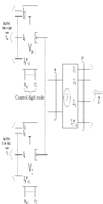
In this paper, the basic logic element of building blocks used in the construction of sequential digital systems is T-gate, and the block diagram for this is shown in Figure 1.
In Figure 1, Ii is the input, Z is the output, Ii, Z=ei∈ GF(Pm) (i=0, 1, 2, ... , Pm-1) and a
http://doi.org/10.33851/JMIS.2019.6.4.323
325
Fig. 1. The block diagram of the Building Block T-gate which is used constructing the sequential logic digital systems.
3.2. Non-feedback sequential circuit implementation
3.2.1. Next state function
When implementing a sequential digital system, the next state function is important.
Also, since sequential digital systems must handle the current state and the next state at the same time, expressing the next state function using time t can be expressed as Equation (7).
St+1= δ [St, It], (7)
where St+1, St, It=ei∈GF(Pm)(i=0, 1, 2, ... , Pm-1). Meanwhile, state S can be assigned as state digit code Vk(k=0, 1, 2, ..., m-1) according to the algorithm for assigning finite elements of Chapter Ⅱ to digit codes, similar to the concept of coding each state into bit codes in the existing sequential digital system in binary. Therefore, after each state is assigned the status digit code, the state expression corresponding to the value from 1 to (P-1) is obtained for each state digit code. The sum of the state and state is the modP sum. In particular, the addition of a GF (2m) of P=2 is mod2 sum, which is possible by the EX-OR calculation. Therefore, the state digit code Vk in finite fields is generated by Vm-1, Vm-2, ..., V1, V0, and the state function according to the Vk value is obtained as Equation (8).
Vkt= (S 0+ S 1 + ... + S ζ-1)t , (8)
where ζ =Pm-1, k=0, 1, 2, ..., m-1, and + is the modP sum. In addition, the sequential status function can be obtained based on the state function (8) obtained earlier from the statement of the previous status indicating the
relationship between the present and the previous state. The above content is expressed in an Equation (9).
S(Vk)t+1=(S 0+ S 1 + ... + S ζ-1)t∙I0 +(S 0+ S 1 + ... + S ζ-1)t ∙ I1 + ... + (S 0+ S 1 + ... + S ζ-1)t∙ Iζ-1
= (∑𝐵−1
𝑖=0 Si)t. I0 +(∑𝐵−1𝑖=0 Si)t. I1 +.. + (∑𝐵−1𝑖=0 Si)t. I ζ-1 = ∑𝐻−1
𝑗=0 (∑𝐵−1𝑖=0 Si)t. Ij (9)
Where, B=H=Pm and ζ is Pm-1, and S
i is the state according to the value of Vk. Also, Vk is the state digit code(k=0, 1, 2, ..., m-1), Vk∈{0, 1, 2, ..., P-1}, and Si=ei∈GF(Pm) (i=0, 1, 2, ..., Pm-1). In addition, ∑, + is the modP sum.
3.2.2 Circuit Realization of Sequential Digital System The circuits in sequential digital systems are illustrated in blocks as shown in Figure 2.
Fig. 2. The block diagram of the sequential digital systems over finite field.
326 Sequential circuit realization algorithm is as follow.
STEP 1: The state in the state transition table is tabulated by assigning it as digital code Vk by digit code allocation algorithms.
STEP 2: In the table obtained from STEP1, obtain the state function according to the state digit code Vk.
STEP 3: Obtain the previous table from state transition table.
STEP 4: Based on STEP 2's state function from the previous table obtained from STEP 3, the sequential state function is obtained and the output function is obtained from the goal state of the state transition
STEP 5: Realize contents obtained from STEP 4 as circuit of final sequential digital system
IV. APPLICATION AND COMPARISON AND
REVIEW
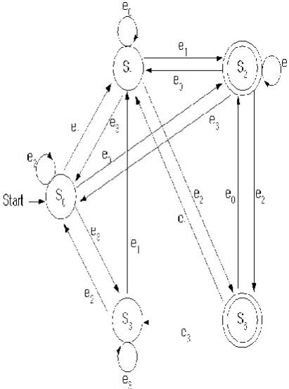
The advanced sequential circuit realization of finite fields, proposed in this paper, was applied for example, and the results were compared and reviewed. From the state transition of finite fields GF (23) as shown in Figure 3, the non-feedback sequential circuit, which is part II of Chapter III, is as follows.
Fig. 3. The state transition diagram over GF (23).
STEP 1 : The state shown in Figure 4 is S0, S1, S2, S3 and S6, and allocating them as state digit code Vk is shown in Table 1.
Table 1. The assignment of states in Fig.5 to state digit codes. state digit code
present state V2 V1 V0
S0 S1 S2 S3 S6
0 0 0
0 0 1
0 1 0
1 0 0
0 1 1
STEP 2 : we obtain the state function are as following Equations (10), (11) and (12).
V2t = (S3)t, (10) V1t = (S2 + S6)t, (11)
V0t = (S1 + S6)t. (12)
STEP 3 : Table 2 shows the previous state table from Figure 3.
Table 2. The predecessor table of Fig. 5. Input
final states
I0 I1 I2 I3
S0 S1 S2 S3 S6
* * S0,S3 S1,S2 S1,S2 S0,S3,S6 * * S0,S6 S1,S2 * * * * * S0,S3,S6 * * S1,S2 *
previous state
STEP 4 : Based on Table 2 which is the previous state table and state function, we are able to obtain the next transition function (13), (14) and (15), also the out-put function is the Equation (16) from goal state in state transition diagram.
S(V2)t+1=(S0 + S3 + S6)t∙I3, (13) S(V1)t+1=(S0+ S6)t∙I0 + (S1 + S2)t∙I1 + (S1+ S2)t∙I2,
(14) S(V0)t+1=
http://doi.org/10.33851/JMIS.2019.6.4.323
327 Zt=(S2 + S6)t. (16)
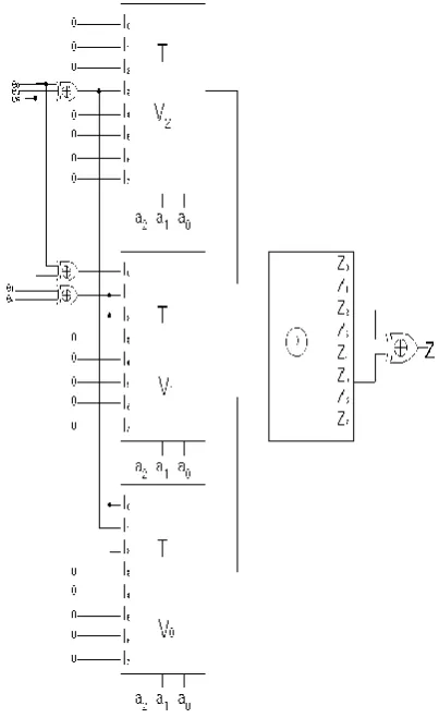
STEP 5 : Using the contents up to STEP4 and Figure 3, the sequential circuits are realized as shown in Figure 4.
Fig. 4. The circuit realization of the sequential digital systems for Fig. 3.
The method of the reference[10] is to implement the concept of universal structure of binary logic by applying it to sequential logic, which has the disadvantages of being applied to all I/O relationships. In generally sequential logic circuits have feedback and are designed using flip-flops, the basic circuit-building elements that can be implemented. The construction of sequential logic circuit over finite fields proposed in this paper has no feed-back and circuit components have designed the circuit using T-gate. This reduces the time required to perform the feed-back and has the advantage of directly obtaining the required output. The hardware comparison of the digital system of the method proposed in this paper and the method cited in this paper is difficult to directly compare because the use element is not the same, but considering the blocks in each sequential digital system as one single element, the comparison is as follows. The reference use the 5 ULM(Universal Logic Module), but this paper use 3 T-gates and 1 decoder. Therefore the
proposed method is more compact and expansible.
Ⅴ. CONCLUSION
In this paper, all elements of finite body were allocated as digit codes using the mathematical properties of finite fields to construct sequential digital system. These digit codes are used as T-gate's control digit code arc(k=0, 1, 2, ... , m-2, m-1), and state digit code Vk(k=0, 1, 2, ...) when configuring sequential digital systems without trajectory. The non-transferable sequential digital system construction method proposed in this paper is summarized as follows. This method allocates the status of the finite body elements presented in Chapter II by the digit code allocation algorithm and obtains the state equation from the conditions according to their values by these state digit codes. Based on the status equation obtained earlier after obtaining the whole table from the status transition, the sequential digital system is configured using T-gate and the device by obtaining the output function from the Goal state. The proposed method does not require complex calculations compared to the computational methods required for the composition of the cited paper. In addition, the number of T-gates is more compact when we construct sequential logic digital systems. For the future, a method (or algorithm) research to implement a more effective sequential logic digital circuit system is needed and is currently under study.
REFERENCES
[1] K. Wong, C. Ysui, S. Cheng, W. Mow, "A VLSI architecture of a K-Best lattice decoding algorithm for MIMO channels", in Proceeding of IEEE Int. Symp. Circuits Syst. (ISCAS), pp. 273-276, 2002.
[2] A. Burg, M. Borgmann, M. Wenk, M. Zellweger, W. Fichtner, H. Bolcskei, "VLSI implementation of MIMO detection using the sphere decoding", IEEE J. Solid-State Circuits, vol. 40, no. 7, pp. 1566-1577, Jul. 2005.
[3] S. Chen, T. Zhang, "Relaxed K-Best MIMO signal detector design and VLSI implementation", IEEE Trans. Very Large-Scale Integr. Syst., vol. 15, no. 3, pp. 328-1337, Mar. 2007.
[4] J. A. Stankovic, "Research directions for the Internet of Things", IEEE Internet Things J., vol. 1, no. 1, pp. 3-9, Feb. 2014.
[5] B. Bollobás, Modern Graph Theory, New York, NY, USA:Springer-Verlag, 1998.
328 [7] Z. Qin, C.-K. Cheng, Symbolic Analysis and
Reduction of VLSI Circuits, New York, NY, USA:Springer, 2005.
[8] R. Lidl, H. Niederreiter, Introduction to Finite Fields and Their Applications, Cambridge, U.K.:Cambridge Univ. Press, 1986.
[9] I. F. Blake, X. Gao, R. C. Mullin, S. A. Vanstone, T. Yaghoobian, A. J. Menezes, Applications of Finite Fields, New York, NY, USA:Springer, 1993.
[10] W. R. E. ‘synthesis of finite state algorithm in a galois field GF(Pm),” IEEE Trans. Comp., vol. C-30, pp.225-229, Mar. 2004.
[11] R. Granger, D. Page, M. Stam, "Hardware and software normal basis arithmetic for pairing-based cryptography in characteristic three", IEEE Trans. Comput., vol. 54, no. 7, pp. 852-860, Jul. 2005. [12] T. Koide, H. Kubo, H. Watanabe, "A study on the
tie-set graph theory and network flow optimization problems", Int. J. Circuit Theory Appl., vol. 32, pp. 447-470, 2004.
[13] E. Fujiwara, Code Design for Dependable Systems: Theory and Practical Applications, 2006.
[14] M. Alioto, G. Palumbo, "Interconnect-aware design of fast large fan-in CMOS multiplexers", IEEE Trans. Circuits Syst. II Exp. Briefs, vol. 54, no. 6, pp. 484-488, Jun. 2007.
[15] M. Iri, Graph Theory With Exercises, Japan, Tokyo: Corona Publ., 1983.
Author
Chun-Myoung Park has received his