A Novel 5 Stage MTCNT Delay Line at 32nm Technology Node
Ambarish Singh Tomar
1, Nikhil Saxena
21
PG Scholar, Department of Electronics & Communication Engineering, ITM Gwalior
2
Assistant professor, Department of Electronics & Communication Engineering, ITM Gwalior
---***---
Abstract -
In this article the practically identicalexamination of discrete parameters of delay line by using MTCMOS and MTCNT systems are finished. After the close examination the results demonstrated that the MTCNT indicated better results when appeared differently in relation to the MTCMOS 10 stages delay line at 32nm advancement layout. Two parameters propagation delay and average power use are moreover processed and looked at. After the connection of parameters it is found that MTCNT delay line has better results when stood out from MTCMOS delay line. The power usage is moreover decreased in the Delay line by using MTCNT when appeared differently in relation to MTCMOS delay line. In the midst of reproduction it is found that the propagation delay of MTCNT delay line diminished by 97.45% then MTCMOS delay line. In this manner it is in like manner evaluated in the midst of reenactment that average power usage of MTCNT delay line diminished by 99.2% when appeared differently in relation to MTCMOS delay line. In any case Voltage using in the midst of both sort of material is similar and settled at 0.7v.
Key words: MT Carbon Nano tube, MTCMOS, Delay line, Power consumption, Propagation delay, Leakage current, Leakage power etc.
1. Introduction
Multi-threshold CMOS (MTCMOS) is a variety of CMOS chip innovation which has transistors with different edge voltages (Vth) so as to upgrade delay or power. The Vth of a MOSFET is the GATE voltage where a reversal layer frames at the interface between the protecting layer (oxide) and the substrate (body) of the transistor. Low Vth gadgets switch speedier, and are in this manner valuable on basic delay ways to threshold clock periods. The punishment is that low Vth gadgets have considerably higher static leakage power. High Vth gadgets are utilized on non-basic ways to decrease static leakage power immediately punishment. Average high Vth gadgets decrease static leakage by 10 times contrasted and low Vth devices.[1]
One strategy for making gadgets with various threshold voltages is to apply different bias voltages (Vb) to the base or mass terminal of the transistors. Different strategies
include altering the GATE oxide thickness, entryway oxide dielectric consistent (material compose), or dopant focus in the channel area underneath the entryway oxide.
A typical strategy for creating multi-threshold CMOS includes just including extra photolithography and particle implantation steps.[2] For a given manufacture process, the Vth is balanced by changing the centralization of dopant iotas in the channel area underneath the entryway oxide. Normally, the focus is balanced by particle implantation technique. For instance, photolithography techniques are connected to cover all gadgets aside from the p-MOSFETs with photoresist. Particle implantation is then finished, with particles of the picked dopant type infiltrating the entryway oxide in regions where no photoresist is available. The photoresist is then stripped. Photolithography techniques are again connected to cover all gadgets with the exception of the n-MOSFETs. Another implantation is then finished utilizing an alternate dopant write, with particles entering the GATE oxide. The photoresist is stripped. Sooner or later amid the resulting creation process, embedded particles are initiated by strengthening at a hoisted temperature.
On a basic level, any number of threshold voltage transistors can be created. For CMOS having two edge voltages, one extra photo masking and implantation step is required for every one of p-MOSFET and n-MOSFET. For manufacture of ordinary, low, and high Vth CMOS, four extra advances are expected with respect to regular single-Vth CMOS.
The most widely recognized usage of MTCMOS for decreasing force makes utilization of rest transistors. Rationale is provided by a virtual power rail. Low Vth gadgets are utilized as a part of the rationale where quick exchanging speed is essential. High Vth gadgets interfacing the power rails and virtual power rails are turned on in dynamic mode, off in rest mode. High Vth gadgets are utilized as rest transistors to decrease static leakage power.
© 2019, IRJET | Impact Factor value: 7.211 | ISO 9001:2008 Certified Journal
| Page 1565
speed, territory, and intensity of a rationale circuit are impacted by the qualities of the power switch.
In a "coarse-grained" approach, high Vth rest transistors GATE the ability to whole rationale blocks.[3] The rest flag is de-attested amid dynamic mode, making the transistor turn on and give virtual power (ground) to the low Vth rationale. The rest flag is affirmed amid rest mode, making the transistor kill and detach power (ground) from the low Vth rationale. The downsides of this approach are that:
• logic squares must be apportioned to decide when a close might be securely killed (on) • sleep transistors are vast and must be
precisely measured to supply the current required by the circuit square
• an constantly dynamic (never in rest mode) power administration circuit must be included
In a "fine-grained" approach, high Vth rest transistors are consolidated inside each logic GATE. Low Vth transistors are utilized for the draw up and pull-down systems, and a high Vth transistor is utilized to entryway the leakage current between the two systems. This approach wipes out issues of rationale square parceling and rest transistor measuring. Be that as it may, a lot of zone overhead is added due both to consideration of extra transistors in each Boolean logic GATE, and in making a rest flag dispersion tree.
A transitional approach is to consolidate high Vth rest transistors into edge logic GATE having more entangled capacity. Since less such edge logic GATE are required to actualize any self-assertive capacity contrasted with Boolean entryways, consolidating MTCMOS into each entryway requires less territory overhead. Cases of threshold entryways having more entangled capacity are found with Null Convention Logic[4] and Sleep Convention Logic.[5] Some craftsmanship is required to execute MTCMOS without causing glitches or different issues.
Many techniques have been proposed to reduce leakage power. Multi threshold CMOS (MTCMOS) technique is an effective circuit level technique to reduce leakage power during standby mode. MTCMOS logic can provide high speed and low power designs without any area overhead. Delay Line with MTCMOS and MTCNT techniques is designed and simulation results are compared here.
As taking reference from MTCMOS, a MTCNT technique is developed in this article. After analysis the MTCNT based delay line circuit, enhancement of result is founded. So by deel analysis of MTCNT & MTCMOS result, it is found that
proposed MTCNT technique have better results than MTCMOS.
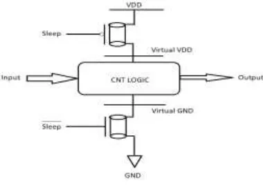
[image:2.612.360.538.222.351.2]In a "fine-grained" approach, high Vth remaining transistors are connected in each Gates. Low Vth transistors are utilized for the circuit ON and OFF systems, and a high Vth transistor is used to Gates the leakage current between the two systems. This technology reduce of issues of apportioning and OFF transistor.
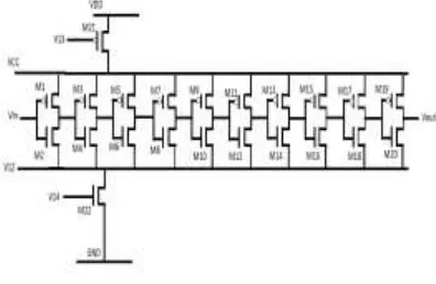
Figure 1: MTCMOS 5 Stage Delay Line
In the figure 1 MTCMOS 5-Stage Delay Line consist a CMOS circuit and also consist extra PMOS and NMOS to make Multi Threshold technique. In figure 1 has consists an input source and also consist two other input are consist that are sleep and sleep bar. When we give 1 input in sleep, this input is going through PMOS transistor is open (OFF) and similarly 0 goes through NMOS transistor then it is sort (ON). Because PMOS transistor is work when input is low (0) and also NMOS transistor is work when input is high (1).
Figure 2: MTCNT 5 Stage Delay Line
[image:2.612.355.545.521.655.2]that are sleep and sleep bar. When we give 1 input in sleep, this input is going through P-type transistor is open (OFF) and similarly 0 goes through N-type transistor then it is sort (ON). Because P-type transistor is work when input is low (0) and also N-type transistor is work when input is high (1).
In the dynamic mode, when SL is set low, Q1 and 42 are turned on and their on-opposition is small to the point that VDDV and GNDV work as genuine electrical cables. In this manner, the NAND door works ordinarily and at a fast on the grounds that the Vth of 0.3 V is sufficiently low with respect to the supply voltage of 1 V. In the rest mode, when SL is set high, Q1 and 42 are killed so the virtual lines VDDV and GNDV are thought to skim. The generally huge spillage present, dictated by the subthreshold qualities of low-vth MOSFET's, is totally stifled by Q1 and 42 since they have a high Vth and along these lines a much lower spillage current. In this manner, control utilization amid the remain by period can be drastically decreased by the rest control.
2. Proposed Technique
Thusly, in this work it is used carbon nanotube field affect transistor rather than silicon in this article, it depicts a delay line circuit which can be used for different sorts of uses. Specifically, we have produced shut circle when can make diverse clock organizes and delays with low jitter, short darting time, and wide jolt go. To achieve this framework objective, a couple of techniques and computations are used as a piece of proposed design. MTCMOS is a term of execution limit which are demonstrated the potential applications are identified with viability electronic properties nearby physical showing. On for creating IC. In 10 stages delay line we are using 10 NOT Gate to impact a delay to settle with NMOS and PMOS to make MTCMOS transistor [1]. It is use 22 transistors and in 10 stage MTCMOS delay line. In the MTCMOS delay line the semiconductor material used that is silicon material. By using of this material and execution of various kind of parameters, for instance, voltage, leakage power, leakage current and propagation delay can be overhauled up beyond what many would consider possible [2]. It is found that decreasing those parameters like as leakage current and power is main problem in demonstrate days. MTCNTFET is one possible response for substitution MTCMOS-based composed circuit advancement, as the execution augmentation of conventional transistors saw in the midst of the latest decades will arrive at its conclusive purposes of imprisonment in the coming future [3]. Its present progress is, as it were, overpowered by the materials science arrange because of various so far existing
materials-related obstacles for recognizing basically engaged transistors. Diverged from grapheme, carbon nanotube gives better properties to building handle impact transistors, and along these lines, has higher shots for over the long haul transforming into an age advancement. based transistor [4]. Basically leakage current and power is the power and current when circuit is thus off condition. In MTCNT strategy we are using Carbon Nano Tube rather than silicon create semiconductor [5]. By using MTCNT leakage current, leakage power and proliferation delay can be increase and execution of circuit can be moved forward. In this article it has been shown that MTCNT transistor is an unrivaled substitution of MTCMOS transistor [8].
2.1 MTCMOS Delay Line :
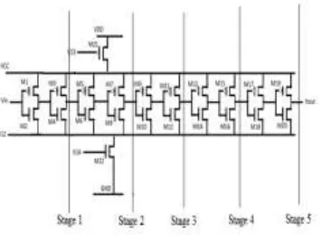
[image:3.612.349.547.383.512.2]In figure 3 show the total no. of transistor is 22 here we use two extra transistor for making multi threshold technique. One transistor is use at the top of CMOS 5-Stage Delay Line and another is use at the bottom of circuit. P-type transistor is used at the top of circuit and N-P-type transistor is used at the bottom of circuit.
Figure 3- MTCOMS Delay Line
© 2019, IRJET | Impact Factor value: 7.211 | ISO 9001:2008 Certified Journal
| Page 1567
Figure 4: 5- Stage MTCMOS Delay LineWhen input voltage Vin=1 then M1 is open (OFF) and M2 will be ON, in that case M1 and M2 together works as a NOT Gate and output of M1 and M2 is 0 and then this output work as an input for M3 and M4 transistors. Then PMOS transistor M3 is ON because the gate terminal of M3 is connected with 0 and NMOS transistor M4 is OFF hence M3 and M4 together works as an Inverter and the output of M3 and M4 is 1. These all four transistors M1, M2, M3 and M4 make a cell known as delay cell because it gives the same output as input. In the proposed circuit it will also works as a first stage out of five stage delay line.
When input voltage of second stage is 1, then transistor M5 is open (OFF) and M6 will be ON, in that case M5 and M6 together works as a NOT Gate and output of M5 and M6 is 0 and then this output work as an input for M7 and M8 transistor. Then PMOS transistor M7 is ON because the gate terminal of M7 is connected with 0 and NMOS transistor M8 is OFF hence M7 and M8 together works as an Inverter and the output of M7 and M8 is 1. These all four transistor M5, M6, M7, and M8 make a cell known as a delay cell because it gives the same output as input. In the proposed circuit it will also works as a second stage out of five stage delay line.
When input voltage for third stage is 1, then transistor M9 is open(OFF) and M10 will be ON, in that case M9 and M10 together works as a NOT Gate and output of M9 and M10 is 0 and then this output work as an input for M11 and M12 transistor. Then PMOS transistor M11 is ON because the gate terminal of M11 is connected with 0 and NMOS transistor M12 is OFF hence M11 and M12 together works as an Inverter and the output of M11 and M12 is 1. These all four transistor M9, M10, M11, and M12 make a cell known as a delay cell because it gives the same output as input. In the proposed circuit it will also works as a third stage out of five stage delay line.
When input voltage for fourth stage is 1, then transistor M13 is open(OFF) and M14 will be ON, in that case M13 and M14 together works as a NOT Gate and output of M13 and M14 is 0 and then this output work as an input for M15 and M16 transistor. Then PMOS transistor M15 is ON because the gate terminal of M15 is connected with 0 and NMOS transistor M16 is OFF hence M15 and M16 together works as an Inverter and the output of M15 and M16 is 1. These all four transistor M13, M14, M15, and M16 make a cell known as a delay cell because it gives the same output as input. In the proposed circuit it will also works as a fourth stage out of five stage delay line.
When input voltage for fifth stage is 1, then transistor M17 is open(OFF) and M18 will be ON, in that case M17 and M18 together works as a NOT Gate and output of M17 and M18 is 0 and then this output work as an input for M19 and M20 transistor. Then PMOS transistor M19 is ON because the gate terminal of M19 is connected with 0 and NMOS transistor M20 is OFF hence M19 and M20 together works as an Inverter and the output of M19 and M20 is 1. These all four transistor M17, M18, M19, and M20 make a cell known as a delay cell because it gives the same output as input. In the proposed circuit it will also works as a fifth stage out of five stage delay line.
Here we find the final output Vout is 1 and we take input Vin is 1. And it shows the 5 Stage CMOS Delay Line.
Table 1 MTCMOS Delay Line Simulation Result
Result of MTCMOS is shown in table 1. Leakage Current of MTCMOS 5-Stage Delay Line is 11.6E-13 Amp, Leakage Power is 81.5E-14 Watt, Average Power is 21.02E-10 Watt and Propagation Delay is 15.1E-11 Sec.
2.2 MTCNT Delay Line (Proposed Circuit)
Converting MTCMOS to MTCNT by changing Carbon Nano Tube in place of silicon.
Parameters 5stage MTCMOS
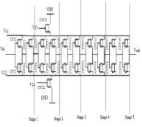
[image:4.612.364.543.466.567.2]Figure 5: MTCNT Based Delay Line
In figure 5 show the total no. of transistor is 22 here we use two extra transistor for making multi threshold technique. One transistor is use at the top of CNT 5-Stage Delay Line and another is use at the bottom of circuit. P-type transistor is used at the top of circuit and N-P-type transistor is used at the bottom of circuit.
In figure 5 transistor CNT21 is a P-type transistor when input is high then the transistor is open (OFF) due to high signal the output is low and this path is closed and leakage is going to down. In this figure (5) transistor CNT22 is also consist with lower part of circuit this is work when input signal is low.
Figure 6: 5-Stage MTCNT Delay Line
When input voltage Vin=1 then CNT1 is open (OFF) and CNT2 will be ON, in that case CNT1 and CNT2 together works as a NOT Gate and output of CNT1 and CNT2 is 0 and then this output work as an input for CNT3 and CNT4 transistors. Then PMOS transistor CNT3 is ON because the gate terminal of CNT3 is connected with 0 and NMOS transistor CNT4 is OFF hence CNT3 and CNT4 together works as an Inverter and the output of CNT3 and CNT4 is 1. These all four transistors CNT1, CNT2, CNT3 and CNT4 make a cell known as delay cell because it gives the same output as input. In the proposed circuit it will also works as a first stage out of five stage delay line.
When input voltage of second stage is 1, then transistor CNT5 is open (OFF) and CNT6 will be ON, in that case CNT5 and CNT6 together works as a NOT Gate and output of CNT5 and CNT6 is 0 and then this output work as an input for CNT7 and CNT8 transistor. Then P-type transistor CNT7 is ON because the gate terminal of CNT7 is connected with 0 and N-type transistor CNT8 is OFF hence CNT7 and CNT8 together works as an Inverter and the output of CNT7 and CNT8 is 1. These all four transistor CNT5, CNT6, CNT7, and CNT8 make a cell known as a delay cell because it gives the same output as input. In the proposed circuit it will also works as a second stage out of five stage delay line.
When input voltage for third stage is 1, then transistor CNT9 is open(OFF) and CNT10 will be ON, in that case CNT9 and CNT10 together works as a NOT Gate and output of CNT9 and CNT10 is 0 and then this output work as an input for CNT11 and CNT12 transistor. Then P-type transistor CNT11 is ON because the gate terminal of CNT11 is connected with 0 and N-type transistor CNT12 is OFF hence CNT11 and CNT12 together works as an Inverter and the output of CNT11 and CNT12 is 1. These all four transistor CNT9, CNT10, CNT11, and CNT12 make a cell known as a delay cell because it gives the same output as input. In the proposed circuit it will also works as a third stage out of five stage delay line.
When input voltage for fourth stage is 1, then transistor CNT13 is open(OFF) and CNT14 will be ON, in that case CNT13 and CNT14 together works as a NOT Gate and output of CNT13 and CNT14 is 0 and then this output work as an input for CNT15 and CNT16 transistor. Then P-type transistor CNT15 is ON because the gate terminal of CNT15 is connected with 0 and N-type transistor CNT16 is OFF hence CNT15 and CNT16 together works as an Inverter and the output of CNT15 and CNT16 is 1. These all four transistor CNT13, CNT14, CNT15, and CNT16 make a cell known as a delay cell because it gives the same output as input. In the proposed circuit it will also works as a fourth stage out of five stage delay line.
[image:5.612.88.234.429.560.2]© 2019, IRJET | Impact Factor value: 7.211 | ISO 9001:2008 Certified Journal
| Page 1569
Inverter and the output of CNT19 and CNT20 is 1. These all four transistor CNT17, CNT18, CNT19, and CNT20 make a cell known as a delay cell because it gives the same output as input. In the proposed circuit it will also works as a fifth stage out of five stage delay line.
3. Results & comparison
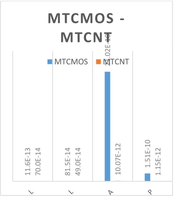
Table:2- MTCMOS Delay Line Result Compared With MTCNT Delay Line:
[image:6.612.73.252.489.691.2]5 Stage MTCMOS and MTCNT delay line are mimicked with the help of SPICE instrument. After recreation it is found that leakage current in MTCMOS 5 stage delay line is 11.6E-13Amp and in the MTCNT 5 organize delay line it is 70.0E-14 Amp, leakage intensity of MTCMOS 5 arrange delay line is 81.5E-14Watt and in the MTCNT 5 arrange delay line is 49.0E-14 Watt, Average power eat up in MTCMOS 5 organize delay line is 21.0E-10Watt and in the MTCNT 5 stage delay line is 10.07E-12 Watt and spread delay found in MTCMOS 5 stage delay line is 15.1E-11 Sec and in the MTCNT 5 stage delay line is 11.5E-13 Sec.
Figure 7: Graph Comparison of Result
Comparison of MTCMOS Delay Line to MTCNT Delay Line given graph show the comparison of leakage current of MTCMOS to leakage current of MTCNT, similarly leakage power, average power and propagation delay show it comparison accordingly.
4. Conclusion
MTCNT transistors have many advantages over silicon based MTCMOS transistor. MTCNT works more effectively and has strong stability for the given parameters like leakage current, leakage control, propagation delay and Average power for MTCNT 5 stage delay line as given in figure (7). It is clear that MTCNT based 5- stage delay line has much better results than MTCMOS based 5- stage delay line. For energize updates in comes about we can use diverse leakage rebat frameworks like SVL, AVL, LECTOR, etc.
5. Acknowledgement
I would like express my deep sense of gratitude and whole hearted thank to all my project mentors for their support, encouragement and valuable guidance. And I would also like thank my parents and friends for the inspiration and help.
6. References
1.
Bilal I. Abdulrazzaq, Izhal Abdul Halin, Shoji Kawahito, Roslina M. Sidek, Suhaidi Shafie, and Nurul Amziah Md. Yunus, A review on high-resolution CMOS delay lines: towards sub-picoseconds jitter performance, 10.1186/s40064-016-2090-z.2.
Abas MA, Russell G, Kinniment DJ. Built-in time measurement circuits—a comparative design study. Comput Digit Tech IET. 2007;1(2):87–97. Doi: 10.1049/iet-cdt: 20060111.3.
Melloni A, Canciamilla A, Ferrari C, Morichetti F, O’Faolain L, Krauss TF, De La Rue R, Samarelli A, Sorel M. Tunable delay lines in silicon photonics: coupled resonators and photonic crystals, a comparison. IEEE Photonics J. 2010;2(2):181–194. doi: 10.1109/JPHOT.2010.2044989.4.
Klepacki K, Pawłowski M, Szplet R. Low-jitter wide-range integrated time interval/delay generator based on combination of period11.6
E-13
81.5
E-14
21.0
2E
-10
1.51
E-10
70.0
E-14
4
9
.0
E-14
10.0
7E
-12
1.15
E-12
MTCMOS -
MTCNT
MTCMOS MTCNT
Parameters 5 stage
MTCMOS delay line
5 stage MTCNT delay line
Leakage Current 11.6E-13 Amp. 70.0E-14 Amp Leakage Power 81.5E-14 Watt 49.0E-14 Watt Average Power 21.02E-10 Watt 10.07E-12Watt Propagation
counting and capacitor charging. Rev Sci Instrum. 2015;86(2):025111. doi: 10.1063/1.4908199.
5.
Kouichi Ishimi, Digital Delay Line, Patent No.: US6,366,150 B1, Apr. 2, 2002.