All-Optical Sampling based on Two-Photon Absorption in a
Semiconductor Microcavity for High-Speed OTDM
P.J.Maguire
aand L.P.Barry
a, T.Krug
b, M.Lynch
b, A.L.Bradley
band J.F.Donegan
b, H.Folliot
ca
Research Institute for Networks and Communications Engineering, School of Electronic
Engineering, Dublin City University, Dublin 9, IRELAND ;
b
Semiconductor Optronics Group, Physics Department, Trinity College, Dublin 2, IRELAND ;
c
Laboratoire de Physique des Solides, INSA, Rennes, FRANCE
ABSTRACT
Future high-speed optical communications networks operating at data rates in excess of 100Gbit/s per channel will require a sensitive and ultrafast technique for precise optical signal monitoring.1 The standard way of characterising high-speed optical signals to use a fast photodetector in conjunction with a high-speed oscilloscope. However, this method is limited to a maximum data rate of approximately 40Gbit/s. An alternative is to employ all-optical sampling techniques based on ultrafast optical nonlinearities present in optical fibres, optical crystals and semiconductors. One such nonlinearity is the optical-to-electrical process of Two-Photon Absorption (TPA) in a semiconductor. This paper presents an optical sampling technique based on TPA in a specially designed semiconductor microcavity. By incorporating the microcavity design, we are able to enhance the TPA efficiency to a level that can be used for high-speed optical sampling.
Keywords: Optical Communications, Optical Time Division Multiplexing, Hybrid WDM/OTDM, Optical Sampling, Two-Photon Absorption, Microcavity
1. HIGH-SPEED OPTICAL MULTIPLEXING TECHNIQUES
Due to the continued growth of the Internet and the introduction of new broadband services such as video-on-demand and mobile telephony, there will be a need to better exploit the enormous bandwidth that optical fibre provides in the network. The conventional method employed by many network providers is to use optical multiplexing techniques to increase the number of carriers per optical fibre. The most common variant, Wave-length Division Multiplexing (WDM), divides up the optical spectrum into a large number of non-overlapping wavelength bands and transmits each individual channel using a different wavelength over a single fibre. To increase capacity in WDM networks, new transmitter/receiver pairing (operating at a different wavelength) can be added, but this is expensive. A second option is to increase the data rate transmitted per channel, but this is limited by the speed of electronics in current integrated circuits. An alternative to multiplexing in the wavelength domain, as in WDM, is to carry out multiplexing in the time domain.
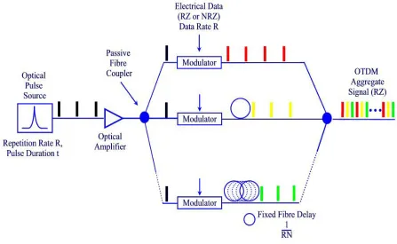
Optical Time Division Multiplexing (OTDM)2 uses short optical pulses to represent data and multiplexes in the time domain by allocating each channel specific bit slots in the overall multiplexed signal. The basic configuration for a interleaved OTDM transmitter is shown in Figure 1. The main component in a bit-interleaved OTDM system is an ultrashort optical pulse source. The optical pulse train generated is at a repetition rate R and is split into N copies by a passive optical coupler, where N corresponds to the number of electrical channels to be multiplexed. Each copy is then modulated by electrical data which is at a data rate R. The resulting output from the modulator is an optical data channel where the electrical data is represented using short optical pulses. The modulated optical signal then passes through a fixed fibre delay length, which delays each channel by 1/RN relative to adjacent channels in the systems. This ensures that the optical data channels arrive at the output at a time corresponding to its allocated bit slot in the overall OTDM signal. The
N modulated and delayed optical data channels are then recombined using a second passive optical coupler to form the OTDM data signal. To increase the overall capacity, shorter optical pulses can be used. However
Figure 1.Bit-Interleaved OTDM Transmission System
as the capacity approaches 1Terabit/s, the duration of the optical pulses used will have to be less than 1ps. The generation of pulses of this type can be complicated and laborious task, and in addition, the dispersion encountered as these optical pulses travel through the fibre may become difficult to compensate for due to their broad spectral width.
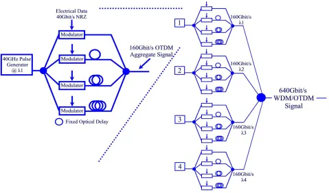
Figure 2.Schematic of the Possible Layout of a 640Gbit/s Hybrid WDM/OTDM Multiplexing Scheme
2. OPTICAL SAMPLING
The standard way of characterising high-speed optical signals utilises a fast photodetector in conjunction with a high-speed sampling oscilloscope. However current electronic monitoring techniques are limited to bandwidths of approximately 80GHz due to difficulties associated with the design of high-speed electronic components.4 These are just capable of accurately measuring data rates of 40Gbit/s, and as individual channel data rates are expected to exceed this by the end of the decade, current electrical sampling techniques will be unable to accurately characterise high-speed data signals. Critical information such as pulse duration, pulse separation and pulse rise-time, which are crucial for the optimisation of the networks performance, will be distorted.
Nonlinear optical effects, which are present in optical fibres, semiconductor devices and optical crystals, occur on time scales in the order of a few femto-seconds (10−15s), and are therefore ideal for performance monitoring and high-speed optical demultiplexing of data. One such nonlinear effect currently being considered for optical sampling takes advantage of Second Harmonic Generation (SHG) in optical crystals. This method involves combining a high-power optical pulse train to the data signal being analysed and generating the mixing product of both signals in the optical crystal. The energy of the mixing product pulse represents the amplitude of the data signal and can be detected by a slow photodetector. Unfortunately there are a number of disadvantages of using the SHG process which may limit its use for optical sampling in a high-speed network. These include:
• Using very high optical intensities for the sampling pulse due to poor efficiency of the SHG process • Stability problems associated with the use of free-space optics
• Need for phase matching at different wavelengths
3. TWO-PHOTON ABSORPTION (TPA)
3.1. TPA Process
Standard semiconductor photodetectors generate a current when incident photons, with energy greater than the band gap of the active region of the photodetector, are absorbed, causing the excitation of an electron from the ground state (valence band) to the excited state (conduction band), resulting in the creation of an electron-hole pair. These are then separated by the electric field present across the active region, resulting in a current (photocurrent) flowing in an external circuit. Individual photons with energy less than the band gap of the photodetector, will not be absorbed, and will not contribute to the photocurrent generated. However, under certain operational conditions, two photons can be simultaneously absorbed to produce a single electron-hole pair. The resulting photocurrent produced is proportional to the square of the incident optical power falling on the detector. This nonlinear optical-to-electrical conversion process is known as Two-Photon Absorption (TPA).5
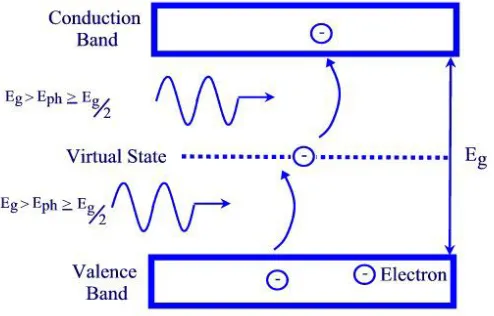
[image:4.595.175.422.363.521.2]TPA was first theoretically proposed when G¨oppert-Mayer, in 1931, described an imaginary third-order nonlinear susceptibility,6 with the first demonstration of the process by Kaiser and Garrett in 1961.7 The TPA process occurs when a photon of energy Eph is incident on the active region of a semiconductor device with a band gap energy exceedingEph but less than 2Eph. Under these conditions, individual photons do not possess sufficient energy to produce an electron-hole pair. However, as stated, an electron-hole pair can be produced by the simultaneous absorption of two photons, were the summation of the individual photon energies is greater than the band gap energy. The absorption of the two photons can be explained using a intermediate virtual state between the conduction band and the valence band within the band gap of the device. This is shown in Figure 3, were the energy of the first photon is used to excite an electron from the valence band to the virtual state, were it is almost instantaneously moved to the conduction band by the energy of a second photon.
Figure 3.Two-Photon Absorption via Intermediate Virtual State
The TPA process needs to be distinguished from a two-step absorption process in which photons are absorbed individually due to linear absorption. Such a process would require a real intermediate state, with a finite lifetime, and it would have a different intensity-dependent absorption relationship.8 TPA involves the simultaneously absorption of two photons via avirtual state, which results in the generated photocurrent being proportional to the square of the optical intensity. It is this nonlinear response, combined with TPA’s ultra-fast response time (10−14s at 1550nm9), that enables TPA to be considered for use in high-speed optical signal processing. The photocurrent produced via the TPA process in a semiconductor pn-junction may be represented by:
I=αISP A+βIT P A2 (1)
material is chosen so that the band gap is greater than the energy of the incident photons but less than twice photon energy. As a result TPA photogeneration will dominate, with only a residual amount of linear absorption due to lattice imperfections or the thermal excitations of carriers with the detector.5
3.2. TPA Microcavity
It has been demonstrated that a commercially available 1.3µm laser diode can be used for the detection of 1.5µm optical pulses via the TPA process.11 Since the band gap of such a device is greater than the energy of the incident photons, there is little chance of single-photon absorption occurring. However, such a device required high optical intensities in order to generate a significant TPA photocurrent. This arises from the fact that TPA is a very inefficient process,12 requiring either high optical intensities typically not found in an optical communications network, or a long interaction length for response enhancement.5 A long interaction length would decrease the response time of the device, limiting its application in high speed OTDM systems. However, by using a Fabry-Perot microcavity structure, the TPA efficiency can be greatly enhanced.
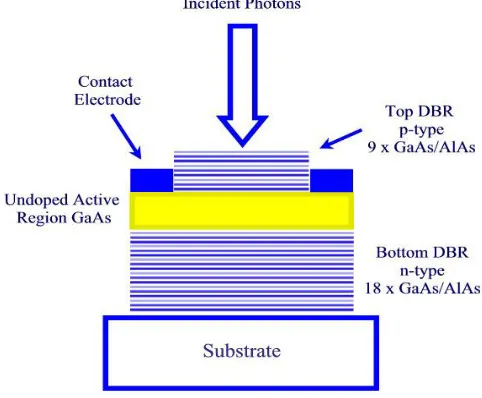
[image:5.595.175.416.346.545.2]The microcavity works by placing mirrors at either end of the active region of the semiconductor, resulting in the formation of very strong optical fields within the cavity. This can be viewed as an increase in the interaction length of the active region. An example of the length-enhancement factor achieved using the Fabry-Perot microcavity is given in,5 where a microcavity with a thickness of 0.3µm has the same response as a 7.5mm long noncavity device. This leads to a reduction in the capacitance of the device, as well as a significant enhancement of the TPA generated photocurrent by four orders of magnitude when compared to noncavity devices.13 Such an increase in the photocurrent should allow the development of a simple and compact device for optical sampling in a high-speed optical communications system. An illustration of the structure of the specially fabricated TPA
Figure 4.Schematic of Microcavity Device Structure
microcavity is shown in Figure 4. It consists of two GaAs/AlAs distributed Bragg reflector (DBR) surrounding an undoped GaAs active region. The active region is 460nm thick with a bandgap energy of 1.428eV.14 The mirrors consist of alternating 134.3nm AlAs and 115.7nm GaAs layers, with the top p-doped (C≈1018cm−3) mirror consisting of 9 periods of AlAs/GaAs whereas the bottom n-doped (Si≈1018cm−3) mirrors consists of 18 periods of AlAs/GaAs. The device length is designed to an integral of the absorption wavelength to enhance the TPA efficiency within the 1.5µm wavelength range, with the cavity lifetime of the device structure, taking into the account of reflectivity of the Bragg mirrors,14 is in the order of 1ps.
jitter of the optical pulses used for the sampling pulse and the signal pulse, and the cavity lifetime of the device, which as mentioned already is a function of the reflectivity of the mirrors used. However, the extraction of the photocarriers produced by the TPA process is affected by the carrier lifetime of the microcavity, which sets a limit to the maximum data rate of the individual channels in the OTDM signal. However, by utilising smaller device sizes, improving the cavity design, and the use of high-speed packaging the bandwidth of the TPA microcavity can be improved to allow high-speed applications.
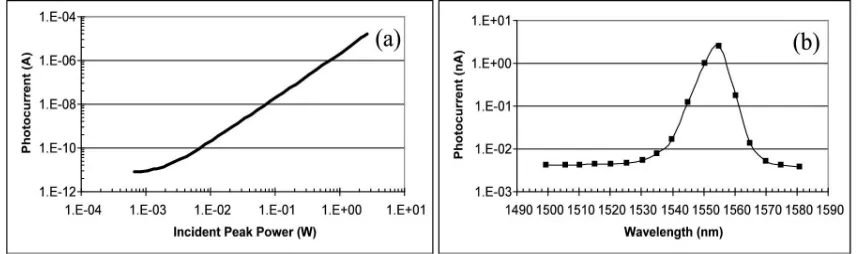
[image:6.595.82.513.232.359.2]For the characterisation of the devices, a photocurrent measurement as a function of the incident optical power close to the cavity resonance (Figure 5(a)) was performed. As clearly shown there is a square dependence of the photocurrent on the incident optical intensity, evidencing the TPA process. The lower side of the response is limited by Single Photon Absorption, whereas the total absorption limits the nonlinear TPA response on the higher intensity side. Figure 5(b) shows how the cavity resonance response is dependent on the incident wavelength, with a cavity resonance of 1554nm and a measured cavity linewidth of 5nm.
Figure 5.(a) Photocurrent as a function of Incident Optical Power (b) Microcavity Resonance
4. PRINCIPLE OF TPA SAMPLING
TPA sampling utilises optical pulses to monitor pulse shape, pulse duration and pulse separation of optical data pulses from a single high speed optical channel. The duration of the optical sampling pulse Isam(t−τ) used must be significantly shorter than the optical signal pulsesIsig(t) under test. The signal and sampling pulses are then incident on the microcavity device and the electrical signali(τ) generated by the TPA process in the device is measured as a function of the sampling delay τ. This results in an intensity cross-correlation measurement betweenIsam andIsig;
i(τ)∝ Isam(t−τ)Isig(t) (2)
where denotes time averaging. For the practical implementation of a TPA sampling system, it is convenient to use a sampling pulse with a peak intensity much larger than the signal intensity. In this case, for a sufficiently short sampling pulse, the measured signal represents the signal pulse waveform on a constant background.15
4.1. Sampling of a Hybrid WDM/OTDM Multiplexing Scheme
high-speed bit-rate. The TPA microcavity then carries out simultaneous filtering and detection of the signal pulse train, with the electrical TPA signal generated by the device measured as a function of the sampling delay. This results in the intensity cross correlation between the data signal and the sampling pulse. In Figure 6, the resonance of the microcavity has been set to the red wavelength channel and this is the only one that experiences any enhancement as all other channels are outside the region of interest. The resulting TPA signal can then be displayed on a low-speed electrical oscilloscope. As the sampling pulse has a shorter duration and higher optical intensity when compared to the signal pulse, and the measured signal represents the signal pulse waveform on a constant background.
Figure 6.Schematic of Possible Sample Set-Up in Hybrid WDM/OTDM Network
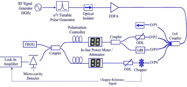
5. EXPERIMENTAL SETUP
Figure 7.Experimental Set-Up for the Sampling of a Qausi-160GHz OTDM Signal
6. EXPERIMENTAL RESULTS
[image:8.595.148.446.452.598.2]Figure 8 (a) compares the pulsewidth and shape obtained using TPA sampling (dotted line) with that measured by the SHG-FROG (solid line) for the same optical pulse. The measured pulsewidth from the TPA sampling was calculated to be∼2.4ps, whereas SHG-FROG measurement recorded at pulsewidth of∼1.7ps. for the same pulse. This deviation can be accounted for by the cavity lifetime of the microcavity,13 and the temporal resolution of the sampling set-up. The temporal resolution of the system is determined by the duration and jitter of the sampling pulses17(tres=(tsam2 +jsam2 )≈2ps). The peak power of the signal and sampling pulses were 2.7mW and 8.6mW respectively. Figure 8 (b) compares the response of both methods for the quasi-160GHz signal. It verifies that the optical pulses were separated by∼7ps highlighting the possibility of using the TPA microcavity for sampling of a 160Gbit/s OTDM signal. The overall system sensitivity was calculated to be 0.1mW2 by determining the minimum optical power levels required to successfully sample the pulse. This corresponds to a signal and sampling peak powers of 1.6mW and 4mW respectively.
CONCLUSIONS
We have shown that by using a microcavity device, we are able to enhance the TPA efficiency to a level that can be used for the successful sampling of a 160Gbit/s optical signal. The sensitivity of the sampling system was calculated ot be 0.1mW2, which corresponds to a signal peak power of 1mW, and a temporal response of ≈2ps. This represents the most sensitive ultra-fast TPA optical sampling system reported, and was achieved without the need for any post-amplification of the electrical TPA photocurrent. With the addition of a low noise electrical amplifier after the detector, the sensitivity should be improved further. Also as the minimum temporal resolution of the system is limited by the duration (1.8ps) and jitter (500fs) of the sampling pulse, the temporal resolution could be further reduced by using shorter duration sampling pulses. Therefore, it is anticipated that all-optical TPA sampling employing a microcavity could have applications for the monitoring of high-speed data signal in future OTDM/WDM communication systems.
ACKNOWLEDGMENTS
This work is supported under Enterprise Ireland’s Advanced Technology Research Programme (ATRP/2002/301a)
REFERENCES
1. S. Kawanishi, “Ultrahigh-Speed Optical Time-Division-Multiplexed Transmission Technology Based on Op-tical Signal Processing,”IEEE Journal of Quantum Electronics 34(11), pp. 2064–2079, 1998.
2. D.M.Spirit, A.D.Ellis, and P.E.Barnsley, “Optical time division multiplexing: systems, networks,” IEEE Communications Magazine32(12), pp. 56–62, 1994.
3. B.K.Mathason, H.Shi, I.Nitta, G.A.Alphonse, J.Abeles, J.C.Connolly, and P.J.Delfyett, “Multiwavelength All-Optical TDM switching using a semiconductor optical amplifier in a loop mirror,” IEEE Photonics Technology Letters11(3), pp. 331–333, 1999.
4. R.L.Jungerman, G.lee, O.Buccafusca, Y.Kaneko, N.Itagaki, and R.Shioda, “Optical Sampling Reveals De-tails of Very High Speed Fiber Systems,” pdf document, Agilent Technologies, www.agilent.com, 2004. 5. H.Folliot, M.Lynch, A.L.Bradley, T.Krug, L.A.Dunbar, J.Hegarty, J.F.Donegan, and L.P.Barry,
“Two-photon-induced photoconductivity enhancement in semiconductor microcavities: A theoretical investiga-tion,”Journal of the Optical Society of America B: Optical Physics19(10), pp. 2396–2402, 2002.
6. N. Bloembergen, “Nonlinear Optics: Past, Present, and Future,”IEEE Journal of Selected Topics in Quan-tum Electronics6(6), pp. 876–880, 2000.
7. W.Kaiser and C.G.B.Garrett, “Two-photon excitation in CaF2:Eu2+,” Physical Review Letters 7(6), pp. 229–231, 1961.
8. H.P.Weber, “Two-photon absorption laws for coherent and incoherent radiation,”IEEE Journal of Quantum Electronics7(5), pp. 189–195, 1971.
9. J. Donegan, “Two-photon absorption speeds optical switching,”Lightwave europeJuly 2002, p. 31, 2002. 10. F.R.Laughton, J.H.Marsh, D.A.Barrow, and E.L.Portnoi, “The Two Photon Absorption Semiconductor
Waveguide Autocorrelator,”IEEE Journal of Quantum Electronics30(3), pp. 838–845, 1994.
11. L.P.Barry, B.C.Thomsen, J.M.Dudley, and J.D.Harvey, “Autocorrelation and Ultrafast Optical Thresh-olding at 1.5µm using a Commercial ingaasp 1.3µm laser diode,” Electronics Letters 34(4), pp. 358–360, 1998.
12. L.P.Barry, P.Maguire, T.Krug, H.Folliot, M.Lynch, A.L.Bardley, J.F.Donegan, J.S.Robert, and G.Hill, “De-sign of microcavity semiconductor devices for highly efficient optical switching, sampling applications,” in Lasers and Electro-Optics Society Annual Meeting-LEOS, Conference Proceedings, Glasgow, 2, pp. 839–840, 2002.
13. H.Folliot, M.Lynch, A.L.Bradley, L.A.Dunbar, J.Hegarty, J.F.Donegan, L.P.Barry, J.S.Roberts, and G.Hill, “Two-photon absorption photocurrent enhancement in bulk algaas semiconductor microcavities,” Applied Physics Letters80(8), pp. 1328–1330, 2002.
15. B.C.Thomsen, L.P.Barry, J.M.Dudley, and J.D.Harvey, “Ultra Sensitive All-optical Sampling Scheme for use in high capacity telecommunication systems at 1.5µm,”Electronics Letters35(17), pp. 1483–1484, 1999. 16. R. Trebino, K. W.DeLong, D. N.Fittinghoff, John.N.Sweetser, M. A.Krumbugel, and B. A.Richman, “Mea-suring ultrashort laser pulses in the time-frequency domain using frequency-resolved optical gating,” Rev. Sci. Instrum - American Institute of Physics68(9), pp. 3277–3295, 1997.