ISSN: 1816-949X
© Medwell Journals, 2019
Characterization of (CIGS)/(CdS) Hetrojunction for Solar Cell
Ikhlas H. Shallal and Balqees A. Ahmed
Department of Physics, College of Education for Pure Science,
Ibn Al-Haitham/Baghdad University, Baghdad, Iraq
Abstract: The CIGS/CdS p-n junction thin films were fabricated and deposited at room temperature with rate
of deposition 5, and 6 nm secG1, on ITO glass substrates with 1mm thickness by thermal evaporation technique
at high vacuum pressure 2×10G5 mbar, with area of 1 cm2 and Aluminum electrode as back contact. The
thickness of absorber layer (CIGS) was 1 µm while the thickness of the window layer CdS film was 300 nm. The X-ray Diffraction results have shown that all thin films were polycrystalline with orientation of 112 and 211 for CIGS thin films and 111 for CdS films. The direct energy gaps for CIGS and CdS thin films were 1.85 and 2.4 eV, respectively. Atomic Force Microscopy measurement proves that both films CIGS and CdS films have nanostructures. The carrier concentration, Hall mobility and the conductivity of CIGS and CdS thin films were calculated by hall effect measurement showing that p = 3.56×10¹⁰ cmG3 and
n = 1.76×10¹⁴ cmG3, respectively. The J-V characteristics for CIGS/CdS solar cells were measured when
illuminated with 1000 W mG2, the efficiency were calculated before and after annealing with
temperature 100 200 and 300°C for one hour in vacuum oven. The results indicate that the efficiency decreases with increasing annealing temperature of CIGS\CdS solar cell.
Keywords: Thin film, hetrojunction, solar cell
INTRODUCTION
In recent years, many studies and researches have been focused on fabrication of Cu (In, Ga) Se2 or (CIGS) solar cells. The CIGS/CdS were considered as excellent materials used to produce hetrojunction and very attractive solar cells devices with high efficiencies and different areas, stable performance, low cost, health hazards and potential in many application possibilities (Bremaud, 2009; Ahrenkiel et al., 1997).
Active layers of CIGS/CdS solar cells can be grown on cheap large area of various substrates including flexible ones and starting from metal foil, non-silicon substrates such as glass, polymer and stainless steel. Typically the most common material used for the back contact is molybdenum (Mo) (especially for soda lime glass substrates) and forms a non-blocking contact with CIGS, also other materials like tungsten (W), tantalum (Ta), manganese (Mn), titanium (Ti), have been used as back contact (Ramanathan et al.,1998; Benmir and Aida, 2013). Variety of deposition techniques used to fabricate CIGS/CdS solar cells such as three stag process method (Ramanathan et al., 1998), thermal evaporation (Benmir and Aida, 2013), vacuum co-evaporation (Singh and Patra, 2010; Gloeckler, 2005), sputtering/selenization, (Urbaniak et al., 2016; Kumari and Verma, 2014), co-sputtering method (Li et al., 2012), i PLD method (Park et al., 2014), chemical bath deposition with efficiencies exceeding 18% (Dong-Sheng et al., 2013; Dhas et al., 2017), electrodeposition (Zhao et al., 2016; Saji et al., 2011),
Physical vapor deposition (PVD) (Cojocaru-Miredin et al., 2011) and spin-coating method (Motoyoshi et al., 2010).Cadmium Sulfide (CdS) thin film plays important n-type absorber material based on CIGS and CdTe thin films (Nakada and Mizutani, 2002; Ramasamy et al., 2017). The CdS is still mostly used as a buffer layer or window layer for CIGS cells and other many p-types absorbers layers like Cu2S, CdTe, InP
because of CdS belongs to n-type semiconductor compounds with wide band gap (2.0-2.42) eV and this leads to fabricate cells with high-efficiency (Mollica, 2016; Mustafa et al., 2017).
The aim of this study is to fabricate solar cells based on Cu (In, Ga) Se2 semiconductor material on ITO glass
substrates and investigate the effect of annealing temperature on the efficiency of Cu (In, Ga) Se2/CdS solar
cells.
Experimental details: Hetrojunction of (CuIn1-xGax)
Se2\CdS were grown on glass substrate with dimension of
1 cm2. All thin film layers of the configuration of solar
cells were deposited using high purity materials, by thermal evaporation technique at room temperature, with thermionic coating unite model (VE.90, USA) at vacuum pressure 2×10G5 mbar. The thickness of absorber layer
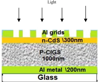
(CIGS) was 1 µm while the thickness of the window layer CdS film was 300 nm. Aluminum (Al) metal was chosen as ohmic contact. Sensitive electric balance type (Mettler H35 AR) is used to weight a certain amounts of the materials. (Fig. 1) illustrate the Schematic diagram Al\(In1-xGax) Se2\CdS\Al thin film solar cell.
The structural properties of CIGS and CdS thin films were investigated using (SHIMADZU diffractometer system (XRD-6000)) Japan, with Cukα wavelength
1.5405. The type of conductivity, Hall mobility (μH), Hall coefficient (RH) was determined from Hall Effect measurement by Hall Effect system type HSM-300. To calculate the energy band gap for CIGS and CdS thin films, the absorption and transmittance spectra were done using UV-Visible spectrometer model UV-2610 in the wavelength range 200-1100 nm. The J-V charact-eristics, short circuit current (Isc), open circuit voltage (Voc), Filling
[image:2.612.92.267.289.434.2]factor (FF) and the efficiency (η) of (Al\CIGS\CdS\Al) solar cell have been measured and reported before and after annealing from 100 and 300°C for one hour in vacuum oven.
Fig. 1: Schematic diagram Al\(In1-xGax) Se2\CdS\Al.
thin-film solar cell
RESULTS AND DISCUSSION
Structural Properties of CIGS and CdS films
XRD analysis For CIGS and CdS films: The structural
identification of CIGS and CdS thin films was examined from the analysis of the X-ray diffraction pattern measured in the range of 2θ between (20o- 60o). Figure 2
shows X-ray pattern of CIGS thin film, from this figure the film structure is Polycrystalline with peaks at 26.6°, 33.8° with orientation 112 and 211, respectively. The preferred orientation 112 diffraction belong to Cu2-xSe
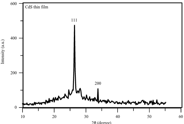
(JCPDS card No. 06-0680) and appearing of 211 is the evidence of the chalcopyrite structure for CIGS thin film. Figure 3 represent the X-ray pattern for CdS thin film deposited on glass substrate, as seen the sharp diffraction peak appears at 2θ equal to 26.50° relating of the 111 cubic planes. These values are matches great with standard information of (JCPDS card no. 10-0454). The grain size was 33 nm. Also notice small peaks with 2θ at 34.95° correspond to (200). These peaks of XRD test demonstrating that the film has polycrystalline with cubic structure.
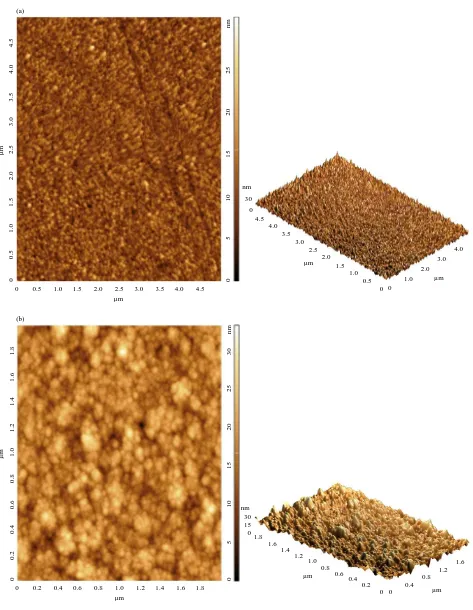
AFM measurement: Surface topography of CIGS and
CdS thin films was studied by AFM, the images of AFM in two and three dimensions of CIGS and CdS thin films shown in Fig. 4. We can see the surface of all samples is uniform and homogenous without any cracks. The measured average surface roughness and root mean square roughness values are listed in Table 1 and show the smooth surface morphology of both films. The average grain size was close to 26 and 33 nm for CIGS
Fig. 2: XRD patterns for CIGS thin film
Light
600
400
200
0
10 20 30 40 50 60 22 (degree)
In
tens
ity
(a.u
.)
[image:2.612.147.455.496.695.2]Fig. 3: XRD patterns for CdS thin film
Table1: Results of AFM measurements
Sample film Grain size (nm) Roughness average (nm) Root mean square (nm)
CIGS film 26.530 3.046 2.417
CdS film 33.203 3.098 3.902
Table 2: Results of hall effect
Film Type RH (m
2
/c) n (cmG3
) μH (cm
2
/V.s)×102
Resisti-vity (Ω.cm)
CIGS p +1.753×10⁸
3.560×10¹¹
3.935 4.456×10⁵
CdS n -3.720×10⁴
1.678×10¹⁵
5.245 7.092×101
and CdS films, respectively, which indicate that the preparing films have a nanostructure. These results of average grain diameter of the films measured from AFM images are found to be in good agreement with the crystallite size obtained using XRD.
Hall effect measurements: Hall effect measurements of
CIGS and CdS thin films have been calculated and the results indicate that CdS films have negative sign of Hall coefficient, while CIGS film have positive sign of Hall coefficient. The data of Hall Effect are reported in Table 2. From this table, the mobilities of both CIGS and CdS films were of the same order of magnitude.
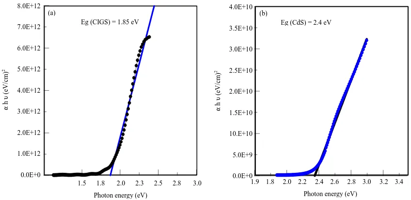
Optical energy gap: The band gap is the first order
parameter in deciding the semiconductor pair for the heterojunction. Based on theoretical considerations, a wide band gap n-type semiconductor with a low series resistance is very essential to make solar cells well. It is seen that a semiconductor with a band gap of about 1.55 eV is ideal for absorber to achieve maximum conversion efficiency. In addition, it should be a direct band gap material with high optical absorption coefficient about 104 cmG1. Khrypunov et al. (2006) From the
transmittance and absorbance spectra, the energy gaps of
CIGS and CdS films have been determined. The energy gap Eg value of the materials is calculated by extrapolation of the straight line of the plot of (αhυ)2
versus photon energy at αhυ = 0, indicating that both materials CIGS and CdS films have direct band gap and the values of energy gap 1.85 and 2.4 eV, respectively, as shown in Fig. 5. It is noticed that the absorption coefficient of CdS and CIGS thin films were increases in the region of high photon energies larger than 2ev.
J-V characteristics of the Al/CIGS/CdS\Al
Configuration: The J-V characteristics of the
Al/CIGS/CdS/Al configuration under illumination were calculated. The photovoltaic parameters which included the short circuit current (ISC), open circuit voltage (Voc), maximum power points (Im, Vm), fill factor (FF) as well as the efficiency (η) were calculated to the as deposited Al/CIGS/CdS/Al and annealed junctions at 100 and 300°C for 1 h in vacuum oven. Hetrojunctions p-(CIGS)/n-type (CdS) have photovoltaic properties and the photocurrent was observed. The efficiency of CIGS/CdS solar cell, decreases from 3.04-1.89% to with increasing annealing temperature from 100, 200 and 300°C. The (J-V) parameters for solar cells made from the CIGS\CdS junction are shown in Table 3.
(111)
(200
)
CdS Thin Film
600
400
200
0
10 20 30 40 50 60
22 (degree)
In
tens
ity
(a.u
.)
200 111
Fig. 4(a-b): Atomic force microscopy images for (a) CIGS film and (b) CdS film 0 0 .5 1 .0 1 .5 2 .0 2 .5 3 .0 3 .5 4 .0 4 .5
0 0.5 1.0 1.5 2.0 2.5 3.0 3.5 4.0 4.5
µm µm 0 5 1 0 1 5 2 0 2 5 n m (a) 0 0 .2 0 .4 0 .6 0 .8 1 .0 1 .2 1 .4 1 .6 1 .8
[image:4.612.77.550.90.700.2]Fig. 5: Variation of (αhŸ)2 versus the photon energy for CIGS and CdS thin films
Table 3: Photovoltaic data for CIGS\CdS solar cells
Sample Annealing temperature (K) Voc (V) Jsc (mA cmG 2
) Vm (V) Im (mA) FF (%) η (%)
S1 RT/298 0.84 3.90 0.46 2.17 30.47 3.04
S2 373 0.32 3.60 0.28 1.97 47.88 2.64
S3 473 0.54 4.86 0.30 2.57 29.37 2.26
S4 573 0.56 2.00 0.46 1.00 41.07 1.89
As shown from this table, the efficiency (η) has different values depending on the annealing temperature. We notice that the values of the efficiency (η) are low in general because of using the vacuum evaporation technique to deposited CdS on CIGS which cause decreases the intermix of Cd-Cu and non stoichiometric CdS formation and the high barrier of electron injection. Decreasing in the values of efficiency after annealing maybe due to the damage in the microstructure of the device. We can improve the efficiency when change the deposition method to chemical bath deposition, one can rise the values of efficiency (Bremaud, 2009; Cojocaru-Miredin et al., 2011).
Photovoltaic device of solar cell made from the CIGS\CdS junction were fabricated and the hetrojunction of p-(CIGS)\n-type (CdS) has photovoltaic properties. The efficiency of CIGS\CdS solar cell, decreases from 3.04-1.89% with increasing annealing temperature from 100-300°C, due to undesirable intermixing of Cd into (CIGS) structure during the elevated temperatures.
CONCLUSION
We can summarize the following conclusions: C The preferred orientation for CIGS thin film is (112)
diffraction which belong to Cu2Se and appearing of (211) is the evidence of the chalcopyrite structure., while the sharp diffraction peak (111) plane for
CdS thin film demonstrating that the film has polycrystalline with cubic structure. The AFM measurement prove that both films CIGS and CdS films have nanostructures
C From hall effect measurement, the mobilities of both CIGS and CdS films were of the same order of magnitude
C Both CIGS and CdS thin films have direct band gap with high optical absorption coefficient about 104 cmG1
ACKNOWLEDGMENTS
I would like to thank the director of solar energy research center Mr. Falah I. Mustafa Al-attar for his assistance. I would also like to thank the other members of the solar energy research center for discussions and help and for their support during the study. This study has been supported by the Ministry of Higher Education and Scientific Research, Baghdad, Iraq.
REFERENCES
Ahrenkiel, R.K., D.H. Levi, S. Johnston, W. Song, D. Mao and A. Fischer, 1997. Photoconductive lifetime of CdS used in thin-film solar cells. Proceedings of the 26th International Conference on Record IEEE Photovoltaic Specialists, September 29-October 3, 1997, IEEE., Anaheim, California, USA., pp: 535-538.
Eg(CIGS)=1.85 eV 8.0E+12
7.0E+12
6.0E+12
5.0E+12
4.0E+12
3.0E+12
2.0E+12
1.0E+12
0.0E+0
1.5 1.8 2.0 2.3 2.5 2.8 3.0
Photon energy (eV)
"
h
L
(eV/cm
)
2
Eg (CIGS) = 1.85 eV (a)
Eg(CdS)=2.4eV 4.0E+10
3.5E+10
3.0E+10
2.5E+10
2.0E+10
1.5E+10
10.E+10
5.0E+9
0.0E+0
1.9 1.8 2.0 2.2 2.4 2.6 2.8 3.0 3.2 3.4
Photon energy (eV)
"
h
L
(eV/cm
)
2
[image:5.612.74.538.343.396.2]Benmir, A. and M.S. Aida, 2013. Analytical modeling and simulation of CIGS solar cells. Energy Procedia, 36: 618-627.
Bremaud, D.J.L., 2009. Investigation and development of CIGS solar cells on flexible substrates and with alternative electrical back contacts. Ph.D. Thesis, ETH Zurich, Zurich, Switzerland.
Cojocaru-Miredin, O., P. Choi, R. Wuerz and D. Raabe, 2011. Atomic-scale characterization of the CdS/CuInSe2 interface in thin-film solar cells.
Applied Phys. Lett., Vol. 98. 10.1063/1.3560308 Dhas, C.R., A.J. Christy, R. Venkatesh, D.D. Kirubakaran
and R. Sivakumar et al., 2017. Effect of sputtering power on properties and photovoltaic performance of CIGS thin film solar cells. Mater. Res. Innovations, 21: 286-293.
Dong-Sheng, C., Y. Jie, X. Fei, Z. Ping-Hua and D. Hui-Wei et al., 2013. Performance improvement of CdS/Cu(In,Ga)Se2 solar cells after rapid thermal annealing. Chin. Phys. B, Vol. 22, No. 1. 10.1088/1674-1056/22/1/018801.
Gloeckler, M., 2005. Device physics of Cu(In,Ga)Se2
thin-film solar cells. Ph.D. Thesis, Colorado State University, Fort Collins, Colorado.
Khrypunov, G., A. Romeo, F. Kurdesau, D.L. Batzner, H. Zogg and A. N. Tiwari, 2006. Recent developments in evaporated CdTe solar cells. Sol. Energy Mater. Sol. Cells, 90: 664-677. Kumari, S. and A.S. Verma, 2014. Buffer layer
selection for CuIn1-x Gax Se2 based thin film solar cells. Mater. Res. Express, Vol. 1, No. 1. 10.1088/2053-1591/1/1/016202.
Li, M., F. Chang, C. Li, C. Xia, T. Wang, J. Wang and M. Sun, 2012. CIS and CIGS thin films prepared by magnetron sputtering. Procedia Eng., 27: 12-19. Mollica, F., 2016. Optimization of ultra-thin
Cu(In,Ga)Se2 based solar cells with alternative
back-contacts. Ph.D. Thesis, Pierre and Marie-Curie University, Paris, France.
Motoyoshi, R., T. Oku, A. Suzuki, K. Kikuchi, S. Kikuchi, B. Jeyadevan and J. Cuya, 2010. Fabrication and characterization of copper system compound semiconductor solar cells. Adv. Mater. Sci. Eng., Vol. 2010. 10.1155/2010/562842.
Mustafa, F.I., Z. Abdsalam and M.A. Jabbar, 2017. Cigs flexible nano solar cell by inert argon gas condensation. Applied Sol. Energy, 53: 167-172. Nakada, T. and T. Mizutani, 2002. 18% efficiency
Cd-Free Cu(In,Ga)Se2 thin-film solar cells
fabricated using Chemical Bath Deposition (CBD)-ZnS buffer layers. Jpn. J. Applied Phys., 41: L165-L167.
Park, S.M., T.G. Kim, Y.D. Chung, D.H. Cho and J. Kim et al., 2014. Junction formation at the interface of CdS/CuInxGa(1-x)Se2. J. Phys. D: Applied Phys., Vol. 47, No. 34. 10.1088/0022-3727/47/34/345302.
Ramanathan, K., H. Wiesner, S. Asher, D. Niles, R.N. Bhattacharya, M.A. Contreras and R. Noufi, 1998. High-efficiency Cu(In,Ga)Se2 thin film solar
cells without intermediate buffer layers. Proceedings of the 2nd International World Conference and Exhibition on Photovoltaic Solar Energy, July 6-10, 1998, National Renewable Energy Laboratory, Vienna, Austria, pp: 1-6.
Ramasamy, M., C.Y. Jung, Y.B. Yeon and C.W. Lee, 2017. Electrochemical atomic layer deposition of Cuin(1-x)GaxSe2 on Mo substrate. J. Electrochem.
Soc., 164: D1006-D1014.
Saji, V.S., S.M. Lee and C.W. Lee, 2011. CIGS thin film solar cells by electrodeposition. J. Korean Electrochem. Soc., 14: 61-70.
Singh, U.P. and S.P. Patra, 2010. Progress in polycrystalline thin-film Cu(In,Ga)Se2 solar
cells. Int. J. Photoenergy, Vol. 2010. 10.1155/2010/468147.
Urbaniak, A., K. Macielak, M. Igalson, P. Szaniawski and M. Edoff, 2016. Defect levels in Cu(In,Ga)Se2
studied using capacitance and photocurrent techniques. J. Phys. Condens. Matter, Vol. 28, No. 21. 10.1088/0953-8984/28/21/215801.
Zhao, Y., J.D. Wu and N. Xu, 2016. Structures, optical absorption and electrical properties of pulsed-laser-deposited CuIn0.8Ga0.2Se2 thin films