warwick.ac.uk/lib-publications
A Thesis Submitted for the Degree of PhD at the University of Warwick
Permanent WRAP URL:
http://wrap.warwick.ac.uk/86733
Copyright and reuse:
This thesis is made available online and is protected by original copyright. Please scroll down to view the document itself.
Please refer to the repository record for this item for information to help you to cite it. Our policy information is available from the repository home page.
Finite Element Electrothermal
Modelling and Characterization of
Single and Parallel Connected
Power Devices
Ji Hu
A thesis Submitted to the University of Warwick
in partial fulfilment of the requirements for the degree of
Doctor of Philosophy
School of Engineering
i
Table of Contents
List of Tables ... v
List of Figures ... vi
Acknowledgements ... xvi
Declaration ... xvii
List of Publications ... xviii
Abstract ... xx
Abbreviations ... xxi
Introduction ... 1
Background ... 1
A Brief History of Power Electronics ... 5
Research Objectives and Contribution ... 6
Outline of Thesis ... 9
Power device modelling ... 11
Introduction to Modelling of Power Semiconductor Devices ... 11
2.1.1 Compact Device Models ... 12
2.1.2 Numerical models ... 13
Compact Models for Power Semiconductor devices ... 14
Transient Thermal Impedance Characteristics and Thermal Modelling of Power devices ... 31
2.3.1 Thermal network in finite element modelling ... 35
Finite Element Modelling of Power Semiconductor Devices ... 38
2.4.1 Continuity equation... 39
2.4.2 The Transport Equations ... 39
2.4.3 Drift-diffusion Transport Model ... 40
2.4.4 Poission’s Equation... 42
2.4.5 Carrier Generation-recombination models ... 42
ii
2.4.7 Impact ionization models ... 45
2.4.8 Heat flow equations in semiconductors ... 46
2.4.9 Contact model ... 47
Finite Element Modelling of Power Devices ... 48
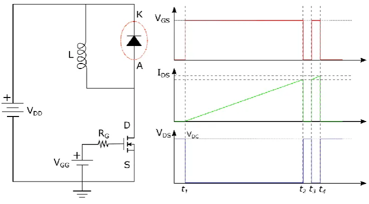
2.5.1 Clamped Inductive Switching Circuit ... 48
2.5.2 PiN Rectifier ... 49
2.5.3 SiC Schottky diodes ... 54
2.5.4 Avalanche Ruggedness under Unclamped Inductive Switching ... 58
2.5.5 Unclamped Inductive Switching of CoolMOS Device... 65
Analysis of Electrothermal Balance in SiC Schottky and PiN Diodes .. 68
3.0 Introduction ... 68
3.1 The experimental set-up ... 73
3.2 Silicon PiN diodes and SiC Schottky diodes under Clamped Inductive Switching Measurements ... 76
a. Silicon PiN diodes in CIS measurements ... 76
b. SiC Schottky diode in CIS measurement ... 79
c. Comparisons of Thermal Transients in Silicon PiN and SiC Schottky Diodes under Repetitive Clamped Switching ... 81
3.3 Electrothermal Balance in Parallel Connected Diodes ... 84
a. Temperature Imbalance ... 84
b. Dynamic behaviour evaluation ... 87
3.4 Electrothermal evaluation of Silicon PiN and SiC Schottky Diodes under Unclamped Inductive Switching ... 90
3.5 UIS measurements and Simulations for Parallel Connected Diodes ... 94
a. UIS measurements on parallel Silicon PiN diodes ... 95
b. UIS measurements on parallel SiC Schottky diodes ... 96
c. Avalanche Ruggedness of the Parallel Pairs with different ΔTJ ... 97
d. Finite Element Modelling ... 101
Conclusion ... 106
Modelling and Experimental Characterization of Parallel Connected Power Devices under Clamped Inductive Switching ... 108
iii
Experimental Set-up ... 111
The Impact of Switching Rate Mismatch ... 114
Finite Element Simulations of Switching Rate Mismatch between Parallel DUTs ... 123
Impact of Initial Junction Temperature Mismatch ... 128
Finite Element Simulations of Initial Junction Temperature Mismatch... 132
Impact of Temperature Variations on Parallel Connected NPT IGBTs ... 136
Impact of Switching Rate Variations on Parallel Connected NPT IGBTs ... 141
Impact of Variations in Case-to-Ambient Thermal Resistances and Capacitances (Different Heatsink Thermal Transients) ... 143
Conclusions ... 148
Implications for Power Electronic Applications ... 151
Electrothermal ruggedness of parallel connected sic mosfet and coolmos ………152
Introduction ... 152
Electrothermal Ruggedness of Power MOSFETs under Unclamped Inductive Switching ... 156
Experimental Test-Rig ... 163
Compact Model Estimation for Junction Temperature of Power MOSFETs under UIS ... 167
Finite Element Simulation of UIS in Parallel Connected DUTs ... 170
Unclamped Inductive Switching Measurements on Parallel Connected DUTs (Impact of Junction Temperature Variation). ... 176
Finite Element Simulation of UIS in Parallel Connected DUTs (Impact of Junction Temperature Variation) ... 181
Impact of Variation in Switching Rates between the Parallel DUTs on Avalanche Ruggedness ... 190
Finite Element Simulations of the Impact of Different Switching Rates ... 194
Conclusions ... 199
Implications for Power Electronic Applications ... 201
Conclusions and future work ... 202
iv
Implications of the Thesis Findings for The Industrial Applications of Power
Electronic Devices ... 205
Future Work ... 209
v
List of Tables
Table 2-1: Loss classification and corresponding equations. ... 30
Table 2-2: The value of the thermal resistance and thermal capacitance in the matched
foster network... 38
Table 4-1: Temperature Rise look up table for parallel-connected SiC MOSFETs
switched with different gate resistance. ... 122
Table 4-2: Temperature Rise look up table for parallel-connected CoolMOS devices
switched with different gate resistance. ... 122
Table 4-3: Parameters of the simulated finite element model. ... 123
Table 5-1: The intrinsic carrier concentration as a function of temperature for silicon and
SiC. ... 163
vi
List of Figures
Figure 2.1: The electric field distribution of the PiN diode. ... 14
Figure 2.2: The reverse recovery characterize waveform for the PiN diode. ... 17
Figure 2.3: Vertical Diffusion MOSFET structure. ... 20
Figure 2.4: Switching characteristic waveforms for the MOSFET with clamped inductive load. ... 24
Figure 2.5: A Comparison of electric field distribution for the MOSFET and CoolMOS. ... 25
Figure 2.6: The breakdown voltage as a function of doping balance for CoolMOS. ... 26
Figure 2.7: PT and NPT IGBT structure. ... 27
Figure 2.8: The schematic of thermal equivalent elements... 32
Figure 2.9(a): The Cauer thermal network schematic. ... 34
Figure 2.10: The thermal model of device in FEM model. ... 36
Figure 2.11: The schematic of clamped inductive switching circuit and waveforms. .... 48
Figure 2.12: (a) the 2-D structure plot for the PiN diode and (b) Electric field distribution at breakdown voltage. ... 50
Figure 2.13: The carrier distribution for different on-state current density. ... 50
Figure 2.14: (a) The turn-On current transient waveform for the PiN diode. (b) The carrier distribution in the drift region corresponding to point V to Z in 2.14(a). ... 51
Figure 2.15: The electric field distribution in the drift region corresponding to point V to Z in Figure 2.14(a). ... 51
Figure 2.16: Diode reverser recovery waveform as a function of (a) switching rate and (b) forward current rating. ... 52
Figure 2.17: Diode reverser recovery waveform as a function of temperature and supply voltage. ... 53
Figure 2.18: (a) Simulated Reverse recovery waveform for the PiN diode. (b) The carrier distribution within the drift region for the PiN diode corresponding to point A, B, C, D and E... 54
Figure 2.19: (a) The SiC Schottky diode model rated at 600V. (b) The electric field distribution at its breakdown voltage. ... 55
Figure 2.20: The (a) simulated turn-Off voltage and (b) simulation circuit. ... 57
vii
Figure 2.22: The measured (a) turn-On and (b) turn-Off transient characteristics for the
SiC MOSFET. ... 58
Figure 2.23: The simulated (a) turn-On and (b) turn-Off transient characteristics for the
SiC MOSFET. ... 58
Figure 2.24: Shorted base-emitter BJT within the VD-MOSFET structure. ... 59
Figure 2.25: UIS test rig and avalanche measurements on a SiC Power MOSFET. ... 60
Figure 2.26: (a) UIS Measurements for a SiC Power MOSFET at different temperatures.
(b) Picture of the device after BJT latch-up. ... 61
Figure 2.27: (a) The layout of the simulated 600V silicon MOSFET, (b) the simulated
avalanche current for the SiC MOSFET which failed in UIS and (c) Corresponding drain
voltage characteristics. ... 63
Figure 2.28: Simulated (a) Avalanche Power and (b) Highest Lattice Temperature of the
Power MOSFET under UIS. ... 63
Figure 2.29: The simulated 2-D current density contour plot for the 600V silicon
MOSFET corresponding to point A, B, C and D in Figure 2.27(b). ... 64
Figure 2.30: The measured UIS waveform for the CoolMOS and conventional MOSFET
at room temperature. ... 66
Figure 2.31: (a) The layout of the simulated 600 V silicon CoolMOS device, (b) the
simulated avalanche current and (c) voltage characteristics of the CoolMOS device. ... 66
Figure 2.32: The simulated avalanche characteristic for the CoolMOS under in UIS
corresponding to point A, B, C and D in Figure 2.31(b). ... 67
Figure 3.1: (a) the clamped inductive switching schematic and (b) unclamped inductive
switching schematic. ... 74
Figure 3.2: The measured (a) turn-ON and (b) turn-OFF transient waveform of power PiN
diode in a clamped inductive switching measurement. ... 77
Figure 3.3: The measured turn-OFF transient waveform of Silicon PiN diode showing the
Transient Characteristics of the (a) IAK, (b) VAK, (c) VGS and (d) IG. ... 78
Figure 3.4: The measured (a) turn-ON and (b) turn-OFF transient waveforms of SiC
Schottky diode in clamped inductive switching measurement. ... 80
Figure 3.5: The measured turn-OFF transient waveform of the SiC Schottky diode
showing (a) IAK, (b) VAK, (c) VGS and (d) IG. ... 80
Figure 3.6: The measured turn-on waveform of the driver MOSFET switched with (a)
PiN diode operating at different temperatures. (b) Similar measurement for the MOSFET
viii
Figure 3.7: The measured (a) turn-on and (b) turn-off switching energy of the MOSFET
as a function of diode operation temperature. ... 82
Figure 3.8: The measured case temperature rise for the (a) PiN diode switched with
different duty ratios. (b) Similar measurement for the SiC Schottky diodes. ... 83
Figure 3.9: The case temperature rise as a function of switching frequency for both the
silicon PiN and SiC Schottky diodes. ... 83
Figure 3.10: The measured (a) turn-ON and (b) turn-OFF current waveforms of parallel
connected PiN diodes with junction temperatures of 25 °C and 100 °C. ... 85
Figure 3.11: The measured (a) turn on and (b) turn off current waveform of the parallel
connected SiC Schottky diodes with junction temperatures of 25 °C and 100 °C
respectively. ... 85
Figure 3.12: The measured (a) turn-ON and (b) turn-OFF switching energies of the
parallel connected PiN diodes as a function of the difference in junction temperature. . 87
Figure 3.13: The measured (a) turn-ON and (b) turn-OFF switching energies of the
parallel-connected SiC Schottky diodes as a function of the difference in junction
temperature. ... 87
Figure 3.14: The measured case temperature rise for the (a) parallel-connected PiN diodes
switched with same heatsink but with 3 °C difference in initial temperature. (b) Similar
measurement for the parallel connected SiC Schottky diodes. ... 89
Figure 3.15: The measured case temperature rise for the (a) parallel-connected PiN diodes
switched with different size heatsinks. (b) Similar measurement for the parallel connected
SiC Schottky diodes. ... 89
Figure 3.16: (a) UIS characteristics of a 600 V SiC Schottky diode and (b) UIS test with
different pulse width. ... 91
Figure 3.17: UIS Current waveform of (a) PiN diode and (b) SiC Schottky diode failure
under avalanche mode conduction. ... 91
Figure 3.18: The maximum avalanche current for different current rated (a) PiN diodes
and (b) SiC Schottky diodes at different junction temperatures. ... 92
Figure 3.19: (a) The measured peak avalanche current and (b) calculated avalanche
energy for the 4A SiC Schottky diode as a function of junction temperature for different
avalanche durations. ... 93
Figure 3.20: Avalanche current characteristics for the parallel SiC Schottky diodes with
ix
Figure 3.21: (a) Avalanche current waveforms for the parallel PiN diodes with different
junction temperatures showing (a) no thermal runaway at 3 A peak current (b) thermal
runaway at 10 A peak current. ... 95
Figure 3.22: (a) Avalanche current waveforms for the parallel SiC Schottky diodes with
different junction temperatures showing (a) no thermal runaway at 8 A peak current (b)
thermal runaway at 8.5 A peak current. ... 97
Figure 3.23: The peak avalanche current as a function of temperature difference between
the parallel connected (a) silicon PiN diodes and (b) SiC Schottky diodes for two inductor
sizes: 1 mH and 3 mH. ... 98
Figure 3.24: The measured avalanche energy dissipated in the (a) SiC parallel Schottky
pairs and (b) Silicon PiN diode pairs as a function of temperature difference between the
DUTs. Measurements for 1 mH and 3 mH inductance. ... 99
Figure 3.25: (a) The measured breakdown voltages of the silicon PiN and SiC Schottky
diodes as functions of temperature (b) Normalised breakdown voltages. ... 101
Figure 3.26: (a) The layout of the simulated 600 V silicon PiN diode, and (b) the simulated
avalanche current for the parallel connected PiN diodes with different junction
temperatures. ... 102
Figure 3.27: 2-D current density plots for parallel connected PiN diodes with different
junction temperatures under UIS. This corresponds to point X in Figure 3.26. ... 103
Figure 3.28: 2-D current density plots for parallel connected PiN diodes with different
junction temperature under UIS. This corresponds to point Y in Figure 3.26. ... 103
Figure 3.29: 2-D current density plots for parallel connected PiN diodes with different
junction temperature under UIS. This corresponds to point Z in Figure 3.26 where the
cooler PiN diode fails to dissipate the avalanche current. ... 103
Figure 3.30: The layout of simulated 600 V SiC Schottky diode. ... 105
Figure 3.31: 2-D current density plots for parallel SiC Schottky diodes with different
junction temperature under UIS. This corresponds to point Y in Figure 3.26. ... 105
Figure 3.32: 2-D current density plots for parallel SiC Schottky diodes with different
junction temperature under UIS. This corresponds to point Z in Figure 3.26 where the
SiC Schottky diode pair fails to dissipate the avalanche current. ... 105
Figure 4.1: (a) Circuit schematic for the experimental set-up. (b) shows the picture of the
experimental set-up with [1] Power Supply. [2] Test Chamber. [3] Function Generator.
[4] Current probe Amplifier. [5] Oscilloscope. [6] Thermometer. [7] DC power supply
for heater. [8] DC capacitor. [9] and [13] Current Probes. [10] and [12] Gate Drives. [11]
x
Figure 4.2: (a) Current switching transient characteristics for the parallel connected SiC
power MOSFETs at turn-ON under balanced conditions (b) Similar measurements for
turn-OFF. ... 113
Figure 4.3: (a) Current switching transient characteristics for the parallel connected SiC
power MOSFETs at turn-ON driven with 2 ns delay between the gate drivers (b) Similar
measurements for turn-OFF. ... 113
Figure 4.4: (a) Turn-ON current waveforms for parallel connected SiC MOSFETs with
different switching rates. (b) Similar characteristics for the CoolMOS device. ... 115
Figure 4.5: (a) Turn-OFF current waveforms for parallel connected SiC MOSFETs with
different switching rates. (b) Similar characteristics for the CoolMOS device. ... 116
Figure 4.6: The measured turn-ON switching energies of the parallel connected SiC
MOSFET as a function of the difference in gate resistance. ... 116
Figure 4.7: The measured turn-ON switching energies of the parallel connected CoolMOS
devices as a function of the difference in gate resistance. ... 117
Figure 4.8: The measured turn-off switching energies of the parallel connected SiC
MOSFET as a function of the difference in gate resistance. ... 118
Figure 4.9: The measured turn-off switching energies of the parallel connected CoolMOS
devices as a function of the difference in gate resistance. ... 118
Figure 4.10: (a) The measured case temperature rise for the parallel connected SiC
MOSFETs switched with RG of DUT1 and DUT2 as 10 Ω and 33 Ω respectively. (b)
Similar measurements for the CoolMOS device. ... 119
Figure 4.11: The measured case temperature rise for the parallel connected SiC
MOSFETs switched at different rates. ... 120
Figure 4.12: The measured case temperature rise for the parallel-connected CoolMOS
devices switched at different rates. ... 121
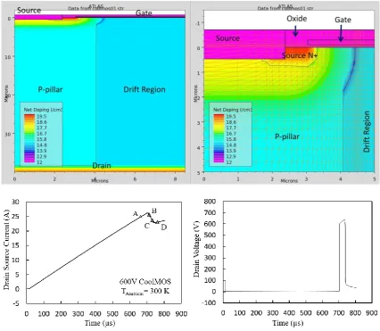
Figure 4.13: SiC MOSFET TCAD Model showing the doping profile and the meshes.
... 124
Figure 4.14: CoolMOS TCAD Model showing the doping profile and the meshes. ... 124
Figure 4.15: The simulated current waveforms for the parallel connected SiC MOSFETs
switched with different gate resistance. ... 125
Figure 4.16: The simulated (a) turn-ON and (b) turn-OFF current waveforms for the
parallel connected SiC MOSFET switched with different gate resistance. ... 126
Figure 4.17: The 2-D current density contour plot for the parallel connected SiC
xi
Figure 4.18: The 2-D current density contour plot for the parallel connected SiC
MOSFETs with different switching rate corresponding to point Y in Figure 4.16(b). . 126
Figure 4.19: (a) turn-ON and (b) turn-OFF current waveforms for the parallel-connected
CoolMOS devices switched with different gate resistance. ... 127
Figure 4.20: The 2-D current density contour plot for the parallel connected CoolMOS
devices with different switching rate corresponding to point X in Figure 4.19(a). ... 128
Figure 4.21: The 2-D current density contour plot for the parallel connected CoolMOS
devices with different switching rate corresponding to point Y in Figure 4.19(b). ... 128
Figure 4.22: (a) The measured turn-ON current for the parallel connected SiC MOSFETs
driven at 2 different junction temperatures. (b) Similar measurements for the CoolMOS
device. ... 129
Figure 4.23: Measured turn-ON switching energy for the parallel connected SiC
MOSFETs with the DUTs set at different junction temperatures. ... 130
Figure 4.24: Measured turn-on switching energy for the parallel-connected CoolMOS
devices with the DUTs set at different junction temperatures. ... 130
Figure 4.25: Measured turn-OFF switching energy for the parallel connected SiC
MOSFETs with the DUTs set at different junction temperatures. ... 131
Figure 4.26: Measured turn-Off switching energy for the parallel-connected CoolMOS
devices with the DUTs set at different junction temperatures. ... 132
Figure 4.27: The simulated current waveforms for the parallel connected SiC MOSFETs
switched at different initial junction temperatures. ... 133
Figure 4.28: The simulated (a) turn-ON and (b) turn-OFF current waveforms for the
parallel connected SiC MOSFETs switched with different initial junction temperatures.
... 134
Figure 4.29: The 2-D current density contour plot for the parallel connected SiC
MOSFETs switched at different junction temperature corresponding to point X in Figure
4.26(a). ... 134
Figure 4.30: The 2-D current density contour plots for the parallel connected SiC
MOSFETs switched at different junction temperature corresponding to point Y in Figure
4.26(b). ... 134
Figure 4.31: The simulated (a) turn-ON and turn-OFF currents for the parallel connected
CoolMOS devices switched at different initial junction temperatures. ... 135
Figure 4.32: 2-D current density contour plot for the parallel connected CoolMOS devices
switched at different junction temperatures corresponding to point X in Figure 4.31(a).
xii
Figure 4.33: 2-D current density contour plots for the parallel connected CoolMOS
devices switched at different junction temperatures corresponding to point Y in Figure
4.31(b). ... 135
Figure 4.34: The measured current waveform of parallel-connected IGBTs switched with
different initial junction temperatures (25 ºC and 55 ºC). ... 137
Figure 4.35: The measured current waveform of parallel connected IGBTs switched with
different junction temperatures (a) Junction temperature of DUT1=25 ºC and DUT2=55
ºC (b) Junction temperature of DUT1=25 ºC and DUT2=105 ºC. ... 138
Figure 4.36: The measured (a) turn on and (b) turn off waveform of parallel connected
IGBTs switched at different initial junction temperature. ... 138
Figure 4.37: The measured turn-ON switching energies of the parallel-connected IGBT
devices with the DUTs set at different junction temperatures. ... 140
Figure 4.38: The measured turn-off switching energies of the parallel-connected IGBT
devices with the DUTs set at different junction temperatures. ... 140
Figure 4.39: Measured (a) turn-on and (b) turn-off current waveform for parallel
connected IGBTs with different switching rates. ... 141
Figure 4.40: Measured turn-ON switching energy for the parallel connected IGBT devices
with the DUTs driven at different switching rates. ... 142
Figure 4.41: Measured turn-off switching energy for the parallel-connected IGBT devices
with the DUTs driven at different switching rates. ... 143
Figure 4.42: The measured case temperature rise for the parallel-connected IGBTs
switched at different rates. ... 143
Figure 4.43: The measured case temperature rise for the parallel connected CoolMOS
devices switched with different heatsinks. ... 145
Figure 4.44: The measured case temperature rise for the parallel connected SiC
MOSFETs switched with different heatsinks. ... 145
Figure 4.45: The measured case temperature rise for the parallel connected SiC
MOSFETs switched with different heatsink. ... 148
Figure 4.46: Percentage change in the turn-ON switching energy (ESW ON) as a function of
the switching rate difference (ΔRG) between the parallel DUTs. ... 149
Figure 4.47: Percentage change in the turn-OFF switching energy (ESW OFF) as a function
of the switching rate difference (ΔRG) between the parallel DUTs. ... 150
Figure 4.48: Percentage change in the turn-ON switching energy (ESW ON) as a function of
xiii
Figure 4.49: Percentage change in the turn-OFF switching energy (ESW OFF) as a function
of the junction temperature difference (ΔTJ) between the parallel DUTs. ... 151
Figure 5.1: MOSFET structure with parasitic components and equivalent circuit. ... 157
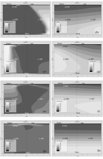
Figure 5.2: Power MOSFET cell (a) without and (b) with deep-body implant. ... 161
Figure 5.3: (c) Typical avalanche characteristics showing the gate voltage, drain voltage
and drain-source current during the charging and avalanche conduction phases. ... 165
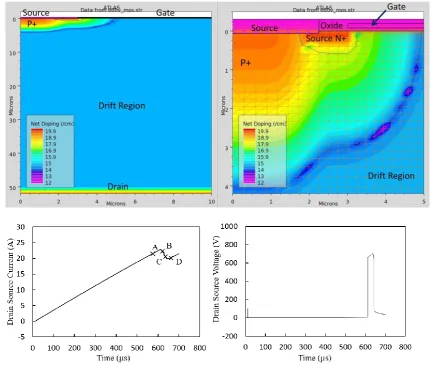
Figure 5.4: (a) UIS measurements of a 1.2kV/10A SiC MOSFET drain-source currents
during the inductor charging and avalanche phases with different gate pulse durations. (b)
The peak avalanche current characteristics of a SiC MOSFET for 2 different inductor
sizes. ... 166
Figure 5.5: Picture of the de-capsulated SiC MOSFETs showing burn mark resulting from
failure under UIS. ... 166
Figure 5.6: The measured maximum sustainable avalanche energy before failure under
UIS for different inductors as a function of temperatures. The device tested was a
1.2kV/24A SiC power MOSFET. ... 167
Figure 5.7: (a) The transient thermal impedance of 1200V SiC MOSFET as a function of
power pulse width; (b) The power dissipated and calculated junction temperature as a
function of time during the avalanche test. ... 169
Figure 5.8: (b) the drain voltage and (c) Avalanche power characteristics of 2 parallel
connected DUTs with identical electro-thermal parameters under UIS. ... 171
Figure 5.9: The Simulated 2-D (a) current density and (b) lattice temperature contour
plots of the parallel connected SiC DUTs at point A corresponding to Figure 5.8(a). . 173
Figure 5.10: The simulated 2-D (a) current density and (b) lattice temperature contour
plots of the parallel connected CoolMOS DUTs at point A corresponding to Figure 5.8(a).
... 175
Figure 5.11: (a) The measured inductor charging and avalanche characteristics for the
parallel connected SiC MOSFETs with different initial junction temperatures. (b)Similar
characteristics for the CoolMOS. ... 177
Figure 5.12: (a) The measured drain source voltage during the charging and avalanche
conduction for the parallel connected SiC MOSFETs with different initial junction
temperatures. (b). Similar characteristics for the CoolMOS. ... 177
Figure 5.13: (a) The measured power loss during charging and avalanche conduction for
the parallel connected SiC MOSFETs with different initial junction temperatures. (b).
xiv
Figure 5.14: (a) The measured peak avalanche currents conducted by the DUTs as a
function of the temperature difference between the parallel connected SiC MOSFETs for
3 avalanche durations (inductance sizes). (b) Similar characteristic for the CoolMOS.
... 179
Figure 5.15: (a) The measured avalanche energy successfully dissipated by the combined
SiC MOSFETs as a function of the temperature difference between the DUTs for 3
avalanche durations (inductor sizes). (b) Similar characteristic for the CoolMOS devices.
... 180
Figure 5.16: Percentage change in the peak avalanche energy (EAV) as a function of the
temperature difference between the parallel DUTs. ... 180
Figure 5.17: The simulated UIS characteristics of 2 parallel connected DUTs at identical
and different initial junction temperatures. ... 182
Figure 5.18: The Simulated (a) Avalanche current; (b) Drain Voltage; (c) Power and (d)
Temperature of the parallel connected DUTs respectively during the UIS. ... 182
Figure 5.19: The simulated (a) 2-D current density and (b) lattice temperature contour
plots for devices with different initial junction temperatures at point W corresponding to
Figure 5.17. ... 183
Figure 5.20: The simulated (a) avalanche current, (b) drain voltage (c) Lattice temperature
and (d) Avalanche power characteristics for parallel connected CoolMOS devices under
UIS at different temperature... 187
Figure 5.21: The simulated 2-D (a) current density and (b) lattice temperature contour
plots for parallel connected CoolMOS devices with different initial junction temperatures
at point X corresponding to Figure 5.20(a). ... 188
Figure 5.22: (a) Avalanche current characteristics for the parallel connected SiC
MOSFETs with different RG. (b) Similar characteristics for CoolMOS. ... 191
Figure 5.23: (a) The measured drain voltage for parallel connected SiC MOSFETs with
different RG. (b) Similar characteristics for CoolMOS. ... 191
Figure 5.24: (a) The measured avalanche power for parallel connected SiC MOSFETs
with different RG. (b) Similar characteristics for CoolMOS. ... 191
Figure 5.25: The measured peak combined avalanche currents conducted by the DUTs as
a function of the switching rate difference between the DUTs for 3 avalanche durations
(inductance sizes) for parallel (a) SiC MOSFETs and (b) CoolMOS devices. ... 192
Figure 5.26: The measured avalanche energy safely dissipated by the combined DUTs as
a function of the switching rate difference between the DUTs for 3 avalanche durations
xv
Figure 5.27: Percentage change in the peak avalanche energy (EAV) as a function of the
switching rate difference between the parallel DUTs. ... 193
Figure 5.28: Simulated UIS characteristics of 2 parallel connected DUTs at the same and
different switching rates. ... 194
Figure 5.29: The simulated 2-D (a) current density and (b) lattice temperature contour
plots for the parallel-connected devices with different switching rates at point X
corresponding to Figure 5.28(a). ... 195
Figure 5.30: The (a) simulated avalanche current (b) drain voltage (c) Temperature and
(d) dissipated power for the parallel connected CoolMOS devices switched with different
gate resistance. ... 197
Figure 5.31: The simulated (a) 2-D current density and (b) lattice temperature contour
plots of the parallel connected CoolMOS with different gate resistances under UIS. This
corresponds to point X in Figure 5.30 where the DUTs are under normal conduction mode.
... 198
Figure 6.1: 1.2 kV/150 A CREE half-bride Power Module implemented in SiC power
MOSFETs and Schottky Barrier Diodes. ... 207
Figure 6.2: 1.2 kV/150 A Fairchild half-bride Power Module implemented in a silicon
xvi
Acknowledgements
The very first and foremost, I would like to sincerely thank my supervisor, Dr. Olayiwola
Alatise, in the University of Warwick. He has been a great teacher, mentor and friend
throughout since four years ago Prof. J. Wang introduced us. I thank you for offering the
PhD opportunity in this group. He has been supportive for this research work with his
extensive and depth knowledge. Moreover, he has showed so much care about my work
and give advises at the right time. And I thank you for so much time and effort you have
spent to revise my papers. I thank you for the time we have been working very hard
together in the summer of 2015 and the outcome is very encouraging.
I would like to thank Jose Angel Ortiz Gonzalez, for not only the technical support
but also the knowledge he has shared with me. He is an expert in long distance running
and swimming, in the meantime with great enthusiasm for his PhD work. I thank you for
propose the idea for my chapter 3, and thank you for the rapid designing of the PCBs and
those machining works in the workshop.
I would like to thank my colleagues, friends in the science city office: Roozbeh
Bonyadi, Petros Alexakis, Fan Li, Han Qin, Ruizhu Wu, Tianxiang Dai and Tianqu Hao.
I thank you for these years of companionship, the fun time we had together, the discussion
we had together, the dinner we had together and the issues we have solved together. I
would like to thank the technicians in the workshop for their rapid and effective work.
Finally, I would like to thank my parents for their support either in moral or in finance.
I would like to thank my girl friend Chenyao Bai for her meticulous care in my daily lives
and encouragement of my PhD work in the past three years. Thank you all!
Ji Hu
xvii
Declaration
This thesis is submitted in partial fulfilment for the degree of Doctor of Philosophy under
the regulations formulated by the School of Engineering of the University of Warwick. I
herewith declare that this thesis contains my own research performed under the
supervision of Dr. Olayiwola Alatise and Prof. Li Ran, without assistance of third parties,
unless stated otherwise. The research materials have not been submitted in any previous
application for a degree at any other university. All sources of information are specifically
acknowledged in the content. The work presented in Chapter 2 has been partly published
in J3, J4 and C5. Majority of the work presented in Chapter 3 has been published in C2
and C3. The work presented in Chapter 4 has been published in J2 and C7. The work
xviii
List of Publications
This section presents the complete list of 1st and co-authored published journal and conference papers by Ji Hu. The 1st author papers result directly from the work presented here.
J1. J. Hu, O. Alatise, J. A. O. González, R. Bonyadi, L. Ran and P. Mawby, "The Effect of Electrothermal Nonuniformities on Parallel Connected SiC Power
Devices Under Unclamped and Clamped Inductive Switching," IEEE Trans.
Power Electron., vol. 31, pp. 4526-4535, 2016.
J2 J. Hu, O. Alatise, J. A. O. González, R. Bonyadi, P.Alexakis, L. Ran and P. Mawby, "Robustness and Balancing of Parallel-Connected Power Devices: SiC
Versus CoolMOS," IEEE Trans. Ind. Electron., vol. 63, pp. 2092-2102, 2016.
C1 J. Hu, O. Alatise, J. A. O. González, P.Alexakis, L. Ran and P. Mawby, "Finite element modelling and experimental characterisation of paralleled SiC MOSFET
failure under avalanche mode conduction," Power Electronics and Applications
(EPE'15 ECCE-Europe), 2015 17th European Conference on, 2015, pp. 1-9.
C2 J. Hu, O. Alatise, J. A. O. González, L. Ran and P. Mawby, "Avalanche Ruggedness of Parallel Connected Diodes: SiC Schottky Diodes vs Silicon PiN
Diodes," submitted to Power Electronics, Machines and Drives (PEMD), the 8th
IET International conference on, accepted 9th Mar. 2016.
C3 J. Hu, O. Alatise, J. A. O. González, L. Ran and P. Mawby, "Comparative Electrothermal Analysis between SiC Schottky and Silicon PiN Diodes:
Paralleling and Thermal Considerations," submitted to Power Electronics and
Applications (EPE'16 ECCE-Europe), 2016 18th European Conference on,
accepted on 1th Mar. 2016.
J3 R. Bonyadi, O. Alatise, S. Jahdi, J. Hu, J. A. O. González, L. Ran and P. Mawby, "Compact Electrothermal Reliability Modeling and Experimental
Characterization of Bipolar Latchup in SiC and CoolMOS Power MOSFETs,"
xix
J4 P. Alexakis, O. Alatise, J. Hu, S. Jahdi, L. Ran, P. Mawby, "Improved Electrothermal Ruggedness in SiC MOSFETs Compared With Silicon IGBTs,"
IEEE Trans. Electron Devices, vol. 61, pp. 2278-2286, 2014.
C4 P. Alexakis, O. Alatise, J. Hu, S. Jahdi, J. A. O. González, L. Ran and P. Mawby., "Analysis of power device failure under avalanche mode Conduction," in Power
Electronics and ECCE Asia (ICPE-ECCE Asia), 2015 9th International
Conference on, 2015, pp. 1833-1839.
C5 R. Bonyadi, O. Alatise, S. Jahdi, J. Hu, L. Evans, and P. A. Mawby, "Investigating the reliability of SiC MOSFET body diodes using Fourier series modelling," in
Energy Conversion Congress and Exposition (ECCE), 2014 IEEE, 2014, pp.
443-448.
C6 J. A. O. González, O. Alatise, N. Nobeen, J. Hu, L. Ran and P.Mawby, "Electrothermal Considerations for Power Cycling in SiC Technologies," in
Integrated Power Electronics Systems (CIPS), 2016 8th International Conference
on, 2016, pp. 1-7.
C7 R. Bonyadi, O. Alatise, J. Hu, Z. Davletzhanova, J. A. O. González, L. Ran and P.Mawby, "Compact Temperature Dependent Physics-Based IGBT Model for
Parallel IGBTs in Clamped Inductive Switching Circuit," in Applied Power
Electronics Conference and Exposition (APEC), 2016 IEEE, 2016.
C8 J. A. O. González, O. Alatise, J. Hu, L. Ran and P. Mawby, "Temperature Sensitive Electrical Parameters for Condition Monitoring in SiC Power
MOSFETs," submitted to Power Electronics, Machines and Drives (PEMD), the
8th IET International conference on, accepted 9th Mar. 2016.
C9 Y. Bonyadi, P. Gammon, R. Bonyadi, O. Alatise, J. Hu, V. Shah and P. Mawby, "The Impact of Triangular Defects on Electrical Characteristics and Switching
Performance of 4H-SiC PiN Diodes," submitted to the 8th Annual IEEE Energy
xx
Abstract
Power modules typically comprise of several power devices connected in parallel for
the purpose of delivering high current capability. This is especially the case in SiC where
small active area and low current MOSFETs are the only option due to defect density
control and yield issues in the epitaxial growth of SiC wafers. Electrothermal variations
between parallel connected devices can emerge from manufacturing variability,
non-uniform degradation rates, variation in gate driving just to mention a few. The impact of
electrothermal variation between parallel-connected devices as a function of device
technology is thus important to consider especially since failure of the power module
requires only failure in a single device. Furthermore, the impact of these electrothermal
variations in parallel-connected devices on the total electrothermal ruggedness of the
power module under anomalous switching conditions like unclamped inductive switching
is important to consider for the different device technologies. In this thesis, the impact of
initial junction temperature variation, switching rates and thermal boundary conditions
between parallel-connected diodes have been evaluated for SiC Schottky and silicon PiN
diodes under clamped and unclamped inductive switching. Finite element simulations
have been used to support the experimental measurements. Similar studies have been
performed in CoolMOS super-junction MOSFETs, silicon IGBTs and SiC power
MOSFETs. New insights regarding the failure of parallel connected devices under
unclamped inductive switching have been revealed from the models and measurements.
Overall, the thesis makes a major contribution in the understanding of the electrothermal
xxi
Abbreviations
ND background doping concentration p Hole concentration
τ
HL Ambipolar carrier lifetime D Ambipolar diffusivityDn(p) Diffusivity for electrons (holes). µn(p) Carrier mobility for electrons (holes).
wd Drift region width
ni Intrinsic carrier concentration AR Effective Richardson’s constant
T Absolute temperature in Kelvin. VFS Bias voltage
𝛷𝐵𝑁 Schottky barrier height k The Boltzmann’s constant Js Saturation current density RCONT Schottky contact resistance
RSUB The resistance in the substrate RD The resistance of the drift region 𝑡𝑂𝑋 Thickness of the gate oxide
𝜀𝑂𝑋 The oxide dielectric constant 𝜀𝑠 Semiconductor dielectric constant
NA Doping concentration in the p-base region ni Intrinsic carrier concentration
LCH Channel length Wcell Cell pitch width
𝜇𝑛𝑖 Inversion layer mobility
COX Specific capacitance of gate oxide 𝑥𝐽𝑃 The P-base junction depth
𝜇𝑛𝐽 The bulk mobility appropriate to the doping level of the JFET region
𝑁𝐷𝐽 Doping concentration in the JFET region W0 Zero-bias depletion width for the JFET region WG Gate width
𝜌𝐷 Resistivity of the drift region
a JFET region width
𝑥𝑃𝐿 Overlap length of gate oxide and p-body region
𝑡𝐼𝐸𝑂𝑋 Oxide thickness between the gate and the source metal JC Total current flow
xxii La Ambipolar diffusion length 𝜆𝑡ℎ Specific heat conductance
c Thermal capacitance 𝜌 The density of material
x The coordinate distance in the direction of heat transfer Gn(p) Generation rates for electrons (holes)
Rn Recombination rates for electrons (holes) TL Lattice temperature
ε Local permittivity ψ Electrostatic potential EG Bandgap energy
NC Effective density of state in the conduction band ρL Local space charge density
NV Effective density of state in the valence band U Recombination rate
Et Trapping energy level
CAΔn High-level injection Auger coefficient Vbi The built-in potential
1
Background
Power electronics has enabled the more efficient and flexible use of electricity. This has
been of benefit to all levels of power conversion ranging from a few watts in low voltage
hand-held electronic devices, to several kilowatts in medium voltage electric drivetrains
for electric vehicles and several giga watts in grid connected converters used in
applications like high voltage direct current (HVDC) converters and flexible AC
transmission systems (FACTS) [1-8].
The increased electrification of heat and transportation coupled with the need to
reduce the reliance on fossil fuels so as to mitigate global warming has made power
efficiency and power electronics a very critical technology. Traditional coal and gas based
power stations are well known for their significant contributions to global warming, hence,
there has been a proliferation of alternate sources of renewable energy including solar and
wind energy conversion systems [9-11]. Connecting these renewable sources of energy
to the power grid requires power electronics to convert a variable voltage variable
frequency AC source to a fixed frequency fixed voltage rating AC delivered to the grid
2
in the case of wind energy conversion systems. Older HVDC systems were based on
thyristor technologies implemented as line commutated current source converters,
however, newer HVDC systems use self-commutated voltage source converters based on
IGBT technology [12-14]. In the case of solar power, a grid tie inverter is required to
convert the DC power generated by the solar cells into single or 3 phase AC power for
grid connection. Furthermore, for long distance power transmission over land or
connection of off-shore wind-farms, HVDC is preferred technology [15, 16]. Power
electronic converters are also useful for connecting asynchronous power systems or even
power systems operating at different frequencies.
Power electronic converters are also the core technology behind the electrification
of vehicle transportation [17]. Traditional internal combustion engines are a key
contributor to greenhouse gas emissions; hence, the drive towards electric vehicles is
important to mitigate climate change. The 2 level 3 phase voltage source converter is
required in electric vehicles for converting the DC electrochemical power stored in the
lithium ion battery to a controllable 3 phase AC voltage for controlling the electrical
machine used for traction [18, 19]. The bi-directional capability of voltage source
converters means that power generating from regenerative breaking can be transferred
back to the battery. The converter is used to control the speed and torque of the machine
through modulation [20]. Power electronic converters are also critical in electric rail
transportation where AC machines are driven and controlled by converters [21]. The
power rating of these converters are typically higher than electric vehicle converters since
greater torque is required. Medium voltage electric drives comprising of back-to-back 2
level 3 phase voltage source converters are also used in ship propulsion [22]. To improve
the efficiency and reduce the carbon emissions of shipping, electric drivetrains are
3
initially used for direct propulsion is instead used to power a generator which supplies
electric power to an electrical motor through a back-to-back power electronic converter.
With increased efficiency and controllability of the electrical motor, energy consumption
can be significantly reduced. Power electronics is also critical in the drive for increased
electrification of aircraft. This is called the More-Electric-Aircraft (MEA) where
functions initially implemented by pneumatic and hydraulic power are increasingly being
replaced with electric power [24, 25]. As aircrafts move towards higher degrees of
electrification, power electronic controllers, breakers and converters will be required for
connecting loads and increasing controllability of the power system.
At the heart of power electronic converters, are the power semiconductor devices
that control power flow to the load through energy storage components like inductors and
capacitors. Power semiconductors act as switches in this manner. Ideally, power
semiconductor devices should have zero on-state loss, zero off-state loss and
instantaneous switching speed, however, this is not possible. The devices have conduction
losses due to series resistances, blocking losses due to leakage current and finite switching
speeds due to parasitic resistances, inductances and capacitances. Power semiconductor
devices can be 2 terminal devices like diodes or 3 terminal devices like transistors and
thyristors. Diodes are passive elements that rectify by conducting in one direction while
blocking in the opposite direction. Transistors are switches that can be controlled either
by current as is the case in a BJT or a voltage as is the case in an FET. While the other
three terminal devices like thyristors are semi-controllable in the sense that they can be
turned ON but not turned OFF [26, 27]. Power semiconductor devices can also be
unipolar devices meaning that carrier flow is due to a majority carrier or they can be
bipolar meaning that carrier flow is due to both majority and minority carriers [26, 28].
4
Thyristors, IGBTs, BJTs and PiN diodes. Power devices can also be classified according
to the semiconductors used to fabricate them. Historically, power devices have been
exclusively silicon based, however, now there are wide bandgap devices based on silicon
carbide and gallium nitride [29, 30].
It is generally well recognised that high power applications use low switching
frequencies while low power applications use high switching frequencies [31-33]. For
example, a switch mode power supply used for connecting a laptop to the mains can run
at switching frequencies in megahertz, while the kilowatt rated converter used in an
electric vehicle will run at a few kHz and the megawatt rated converter used in a modular
multi-level HVDC converter will run at grid frequency (50 Hz or 60 Hz). Hence, high
power low speed applications are usually implemented by thyristors, while low voltage
high speed applications are implemented by discrete power MOSFETs. IGBTs have
become popular for medium voltage medium frequency applications [34]. Thyristors with
voltage ratings as high as 8 kV and current ratings as high as 4 kA are available as phase
controlled thyristors and as typically deployed to line commutated current source
converters for multi-gigawatt HVDC systems [33, 35, 36]. However, wide bandgap
materials like SiC have pushed MOSFETs into the medium voltage arena. Thanks to SiC,
1.2 kV and 1.7 kV power MOSFETs and diodes are now available in TO-247 packages
and as power modules. SiC MOSFETs with breakdown voltages as high as 10 kV and
even 15 kV have been demonstrated by Wolfspeed (formerly CREE) [37, 38]. Gallium
nitride is another wide bandgap semiconductor, however, due to processing issues and
the lack of availability of a bulk GaN substrate, GaN devices are limited in scope and
5
A Brief History of Power Electronics
Solid state power electronic devices were first proposed as a point contact germanium
transistor by Bardeen and Brattain in 1947 [39, 40]. The bipolar junction transistor (BJT),
which was formed as a variable resistance with a third terminal to control the current flow,
was proposed by Shockley [41]. Eventually, such solid state devices were developed and
fabricated in silicon for low cost, hence, vacuum tubes were replaced to improve the cost
performance balance. In the 1950s, power conversion performed by semiconductor
switching devices became a reality. In 1956, the silicon controlled rectifier (SCR) was
introduced by General Electric [42-44]. In the same year, the thyristor became
commercially available. These greatly increased the range of power electronic
applications. In 1976, the vertical power Metal-Oxide-semiconductor field effect
transistor (MOSFET) became commercially available. Due to the insulating gate and
increased controllability, it was an improvement over BJTs. In 1979, the Insulated Gate
Bipolar Transistor (IGBT) was introduced as a hybrid between a MOSFET and a BJT. It
has a MOS input and a bipolar output, thus taking advantages of the ease of controllability
of the MOSFET and the current density capability of the BJT. In 1999, the super-junction
MOSFET became commercially available. This improved the conduction loss
performance of the MOSFET by using the concept of charge balance from alternating p
and n columns to reduce the drift layer thickness. More recent research interest has been
paid to the wide band gap material silicon carbide as it shows superb performance in
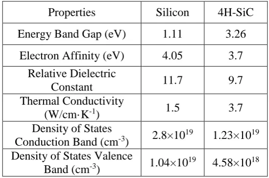
fabricating high power devices than the silicon. Table 1-1 shows the comparison of
fundamental property between silicon and SiC. In 2011, the very first SiC power
MOSFET became commercially available by CREE although the Schottky barrier diode
was first released in 2002. The Schottky diode exhibited significantly reduced switching
6
no reverse recovery current. Today SiC power MOSFET devices and modules are
commercially available from CREE and ROHM. GE also make SiC MOSFETs although
they are not commercially available likewise Mitsubishi. Low current SiC thyristors are
also available from GeneSiC. It is envisaged that over the coming years, the power
handling capability of SiC modules will increase and the cost will decrease, however, this
will be driven by market forces. Nevertheless, there are still significant technology
barriers impeding the realisation of low cost SiC wafers and devices. Stacking faults,
basal plane defects and other crystalline defects associated with SiC limit the wafer yield
and the reduced epitaxial growth rate limits the wafer-line production throughput.
Properties Silicon 4H-SiC
Energy Band Gap (eV) 1.11 3.26
Electron Affinity (eV) 4.05 3.7
Relative Dielectric
Constant 11.7 9.7
Thermal Conductivity
(W/cm·K-1) 1.5 3.7
Density of States
Conduction Band (cm-3) 2.8×10
19 1.23×10¹⁹
Density of States Valence
Band (cm-3) 1.04×10
[image:30.595.188.463.333.515.2]19 4.58×10¹⁸
Table 1-1: Fundamental material properties.
Research Objectives and Contribution
This thesis focusses on the finite element modelling and experimental characterisation of
different power semiconductor devices ranging from silicon PiN diodes, to SiC Schottky
diodes, silicon IGBTs, CoolMOS super-junction MOSFETs and SiC power MOSFETs.
The electrothermal characteristics of these devices under clamped and unclamped
inductive switching conditions have been considered both as single devices and as
7
typically connected in parallel to deliver higher current ratings. They can also be
connected in series for high voltage blocking capability however, this has not been
considered in this thesis. Parallel connection is more so the case for silicon carbide
devices where small area MOSFETs with low current conduction ratings are the only
option. These devices can exhibit electrothermal non-uniformities arising from several
factors including manufacturing variability, gate drive variability, non-uniformities in
circuit parasitic inductances, variability in packaging and non-uniformities in the rate of
device degradation. How these electrothermal variabilities impact energy balance
between the devices will vary from technology to technology. For instance, if
parallel-connected MOSFETs have different switching speeds arising from different gate
resistances, how will this impact the balance of the switching losses between the devices
in transients and in steady state. This is important to consider because it will determine
the overall reliability of the converter since the devices will not be equally stressed, hence,
one device will degrade faster than another. Furthermore, in potentially destructive
switching conditions like unclamped inductive switching, the impact of device-to-device
variability between parallel-connected devices on the overall ruggedness of the power
converter is very important to be considered since the devices are working beyond the
safety operation area (SOA). This thesis also uses finite element simulations to investigate
the electrothermal dynamics between parallel connected devices under balanced and
unbalanced conditions. Lattice temperature and current density plots extracted from the
finite element simulator are used to understand the electrothermal characteristics of the
parallel devices. Specifically, this thesis has
(1) Finite Element modelling of power semiconductor devices including silicon
PiN diodes, SiC Schottky diodes, silicon MOSFET, CoolMOS, IGBT and SiC
8
MOSFET, CoolMOS, IGBT and SiC MOSFET. The internal physics of these
device in avalanche mode conduction is used to understand the experimental
measurements.
(2) A comparison evaluation of the avalanche ruggedness for silicon 600V/20A
MOSFET and silicon 600V/20A CoolMOS device.
(3) A comparative electrothermal analysis between parallel connected SiC
Schottky diodes and parallel connected silicon PiN diodes. The impact of
variation in the switching speed of the complimenting transistor and initial
junction temperature of the devices is investigated for both technologies.
(4) A comparative avalanche ruggedness evaluation between parallel connected
SiC Schottky diodes and silicon PiN diodes. The impact of variation in the
thermal boundary conditions, switching speed and initial junction temperature
on the avalanche ruggedness of the parallel diodes is investigated. Alongside
with finite element modelling characterise the diode failure mode in avalanche
mode conduction.
(5) A comparative electrothermal balancing analysis between parallel connected
CoolMOS, NPT IGBT and SiC MOSFET under clamped inductive switching
conditions. The impact of variation between the thermal boundary conditions
(heatsink thermal resistance), the initial junction temperature and the switching
speed has been analysed for the different technologies for single and repetitive
switching events. Experimental measurements have been confirmed with finite
element modelling of each technology.
(6) A comparative electrothermal ruggedness evaluation between parallel
connected CoolMOS devices and parallel connected SiC MOSFETs. The
9
overall ruggedness performance of the parallel pair is investigated for both
technologies. The failure mechanism and internal physics is modelled and
extracted by the finite element simulator.
Outline of Thesis
Chapter 2 provides a brief introduction to the physics of power semiconductor devices for the different device types. Compact modelling and finite element modelling of the
power devices are introduced. This section of the thesis focuses on finite element
modelling and experimental characterisation of single power devices (transistors and
diodes) under clamped and unclamped inductive switching conditions. The finite element
simulator is used to explain certain characteristics peculiar to certain devices and
experimental measurements are used for confirmation.
Chapter 3 presents the impact of electrothermal imbalance between parallel connected silicon PiN and SiC Schottky diodes under clamped and unclamped inductive switching
conditions. Switching and conduction loss balance between the diodes as a function of
electrothermal variation is investigated for both technologies. Also, the avalanche
ruggedness of the parallel diodes is investigated as a function of electrothermal variation
between the parallel connected pair for both technologies. The results of this chapter have
been reviewed, critiqued and accepted as conference publications and will be presented
in the IET Power Electronics Machines and Drives (PEMD) conference in Glasgow 2016
as well as the IEEE European Power Electronics (EPE) conference held in Karlsruhe,
Germany in 2016.
super-10
junction MOSFETs. The impact of variation in the thermal boundary conditions, initial
junction temperature and switching speeds between the parallel pair have been
investigated for the different technologies. This is supported by finite element simulations
that give insight into the internal physics of the device through 2-D current density and
lattice temperature plots. The methods, analysis and results of this chapter have been
published in the IEEE transactions of power electronics and industrial electronics as first
author papers by the author is this thesis. The results have also been presented in the IEEE
European Power Electronics Conference (EPE) held in Geneva Switzerland in 2015.
In chapter 5, the experimental measurements on the impact of electrothermal variation between parallel connected SiC MOSFETs and parallel connected CoolMOS devices are
presented. This chapter investigates how electrothermal variations affects the avalanche
ruggedness of the parallel connected devices for different technologies. It explores how
this electrothermal variation between the parallel pair degrades the avalanche ruggedness
for different avalanche pulses i.e. high power low duration pulses and low power high
duration pulses. Electrothermal variations between the parallel pair are introduced by
varying the switching rate and initial junction temperature between them. Finite element
simulations are used to support the experimental observations and explain the results. The
methods, analysis and results of this chapter have been reviewed, critiqued and published
as first author journal papers in the IEEE Transactions on Power Electronics and IEEE
Transactions on Industrial Electronics by the author of this thesis. The results have also
been presented in the IEEE European Power Electronics Conference (EPE) held in
Geneva Switzerland in 2015.
11
Introduction to Modelling of Power Semiconductor Devices
Power semiconductor devices are at the heart of power electronic converters. They are
typically two terminal devices like diodes or three terminal devices like transistors or
thyristors. They can be bipolar devices like PiN diodes, BJTs, IGBTs and thyristors or
unipolar devices like MOSFETs and Schottky diodes. The modelling of power devices is
critical for understanding and predicting the energy conversion losses as well improving
reliability. The design loop can be simplified and significant cost saving ensured by using
predictive modelling. Since power devices generate heat as a result of conduction and
switching losses, and device electrical parameters like threshold voltage, on-state
resistance and breakdown voltage are all temperature sensitive, then the device models
must account for the feedback loop between the electrical characteristics and junction
temperature. In other words, the models must be electrothermal. Electrothermal models
can be realized in two major ways: by using (a) behavioural-based model, or by (b)
physics-based model. Behavioural models are empirical in that they are typically derived
from experimental measurements. They can also be reduced forms of more complicated
12
simulations. Behavioural models are computationally inexpensive and are particularly
useful when large systems are simulated in a manner that does not require detailed
physical knowledge of the power device [47, 48]. For example, if a wind energy
conversion system comprised of the rotating electrical generator, gearbox, converter and
transformer were to be simulated, given the time constants of the mechanical components
of the system, a behavioural model of the power devices in the converter will suffice. On
the other hand, the physics based model requires detailed knowledge of the
semiconductor physics behind the operation of the device. This is important for low level
device fabrication, converter design and device reliability modelling. Physics based
models vary in complexity and speed. For example, SPICE models as less
computationally expensive than finite element models, however, cannot account for
certain physical phenomena that finite element models can explain. In general, there is a
trade-off between simulation accuracy and computational cost. The more accurate a
model is, the more computationally expensive it will be.
2.1.1 Compact Device Models
Compact models are more accurate and computationally intensive than behavioural
models but not as accurate as finite element models. The mathematical compact model is
based on solving physics-based equations with varying degrees of complexity thereby
resulting in analytical expressions describing carrier and electrical behaviour.
In the lumped-charge models, carrier dynamics are divided into discrete charges
within the device with the charge of each region being considered as its average charge
[49, 50]. This offers rapid simulation time however at the cost of reduced accuracy. The
13
exploited for the MOSFET [51] and IGBT [52]. The model is capable of simulating the
reverse recovery of the power diode [50].
2.1.2 Numerical models
The ambipolar diffusion equation (ADE) model used in compact model implemented the
semiconductor equations based on the assumption of quasi-neutrality or principle of the
ideal depletion layer behaviour. However, certain non-linear characteristics like the
exponential dependence of carrier density on potential limits the accuracy of compact
models. Therefore, for a high degree of accuracy, numerical schemes such as finite
element or finite difference are good candidates. There are several commercial device
simulators including ATLAS, Sentaurus and Medici [47, 53]. These simulators
decompose the device under study into a pre-defined mesh with each mesh point
investigated individually based on doping level, potential and lattice temperature, etc.
During static and dynamic simulations, the hole and electron carrier density at each mesh
point is used to derive the electric field and current, and is fed back into the neighbouring
mesh points to generate a distributed model. The mesh size must be implemented
carefully to avoid numerical instability due to the discrete nature of the model. The mesh
size also determines the accuracy of the simulation. Fine meshes will result in higher
accuracy but at a cost of reduced computational speed and increased computational cost.
ATLAS from SILVACO is typically used by the semiconductor designers for designing
devices as well as modelling static and dynamic characteristics. Hence in this thesis, all
14
Compact Models for Power Semiconductor devices
Structural design improvements such as trench gates [54, 55], super-junctions [56, 57],
Junction-Barrier-Schottky designs [58, 59] and thick-bottom-oxide/split gate trench
designs [60, 61] in power semiconductor devices have led to increased application range
and improved efficiency of power electronics. Recently released power semiconductor
devices can sustain higher blocking voltage, switching at higher frequencies and exhibit
lower on-state resistance [62-64]. However, these improvements can also cause reliability
problems like ringing, voltage overshoots resulting from high dI/dt and dV/dt, parasitic
turn-on and/or turn-off due to cross-talk between devices. Therefore, accurate compact
models for power semiconductor devices are required by circuit designers to evaluate and
predict circuit behaviour, though, they have limited insight into the internal physics of the
device.
PiN diode
The PiN rectifier is fabricated by simply inserting a lightly doped voltage blocking
epitaxial n layer between a conductive n+ cathode and a conductive p+ anode as shown
in Figure 2.1.
15
PiN diodes are designed for high voltage applications where high blocking voltage
in one direction and high current conductivity in the opposite direction is required. The
on state conductivity is improved by minority carrier injection into the drift region, which
results in charge storage during the on-state. This charge storage in the drift region leads
to non-ideal behaviour like forward and reverse recovery charge during switching
transients. The PiN diode exhibits on-state current conduction mechanisms at different
current level [26]. At very low current density, the recombination current in the
space-charge layer is the dominant component of the current. At low current density, minority
carriers from the highly doped terminals are injected into the drift region and the diffusion
of these carrier dominates the current transported. At high current densities, there is
significant minority carrier injection into the drift region from the p+ region. When the
injected hole concentration into the drift region exceeds the background doping
concentration (ND), charge neutrality requires that the concentration of electrons and
holes must become equal: n(x) = p(x). The excess carrier density in the drift region is
determined by the ADE as [26, 65-67]:
2
2
, , ,
HL
p x t p x t p x t D
x t
(2.1)
where p is the hole concentration;
τ
HL is the ambipolar carrier lifetime; D is the ambipolardiffusivity
2 n p
n p
D D D
D D
(2.2)
where Dn and Dp is the diffusivity for electrons and holes, respectively. The carrier