Control of a Modular Multilevel Converter with
Pulsed DC Load
Marija Jankovic, Alan Watson, Alessandro Costabeber and Jon Clare
Department of Electrical and Electronic EngineeringUniversity of Nottingham Nottingham, UK
Email: [email protected]
Abstract—This paper focuses on a Modular Multilevel Con-verter grid interface for a klystron modulator system that behaves as a pulsed DC load. With such a load, and without mitigating control, the MMC suffers from cell capacitor voltage imbalance between the converter arms which leads to distortion (fluctuation) of the absorbed AC power. This paper proposes an augmented modulation strategy, with a tailored distribution of the modulation signals between the arms within a phase, to ensure low AC power fluctuation. The effectiveness of the method has been verified through simulation and has been experimentally proven on a 7 kW MMC prototype operating with a 3 kA pulsed DC load.
I. INTRODUCTION
The Modular Multilevel Converter (MMC) due to its high modularity, efficiency and good AC waveform quality [1] has been selected as a suitable topology for the grid interface for the klystron modulators used in the Compact Linear Collider (CLIC) [2], [3]. MMCs are typically used in HVDC systems where one of the advantages is the absence of a bulk DC link capacitor. Conversely, in the application of interest, the klystron modulators work in a pulsed mode and are supplied from a capacitor bank that is periodically discharged by the high current pulse. The DC link capacitor is used to suppress pulsed load effects and to limit the DC voltage droop caused by pulsed current to 10% of the nominal value. The main challenge for the grid interface is to further suppress the pulsed load effects on the AC side, by ensuring AC power fluctuation below 2%. The converter and klystron modulator parameters for the proposed system are given in Table I. The passive components are rated in correspondence with [3], [4].
Some of the first research efforts associated with this application were focussed on suppressing the DC power fluctuation by inserting a droop compensator [5]. Another option investigated was to have a high bandwidth controller that would ensure a DC current profile that minimises the DC side power fluctuation [2]. Since the MMC has internal energy storage elements it should be possible to achieve low AC power fluctuation despite the presence of higher DC power fluctuation (more than 10%). A suitable control method is to decouple the AC and DC side control [6], i.e. to decouple the pulsed load from the grid. However, the presence of a 50Hz component in the DC voltage due to the voltage droop (note that the pulse repetition frequency is 50Hz), causes imbalances between the cell capacitor voltages of the upper and lower
TABLE I
CONVERTER AND LOAD PARAMETERS.
Description value
Rated power 16MW
DC voltage 20kV
AC voltage 10kV
Number of cells per arm 20 Nominal cell voltage 1kV
Phase inductance 3.6mH
Arm inductance 1.8mH
Cell capacitance 13mF
DC link capacitance 8mF
DC voltage droop 2kV
Pulse frequency 50Hz
Pulse duration 140µs
arms, which then causes overmodulation and distortion of the AC power. A control method to balance the capacitor voltages was proposed in [7]. This method is based on the addition of a 50Hz component in the circulating current reference in phase quadrature with the 50Hzcomponent of the DC voltage ripple. However, this method is sensitive to the load pulse positions within the AC supply voltage period, and, if the pulse is in a critical region, balancing cannot be performed and AC power fluctuation exceeds the specification. A similar balancing method reported in [8], [9] suggests the insertion of a 50Hz component in the circulating current reference in phase with the AC voltage reference. This method has been proposed for the normal operating mode of the MMC (e.g. HVDC applications) where imbalance between the converter arms is expected only during transients. However, by using appropriate controllers this method can be applied for pulsed DC load applications. Both arm balancing methods require circulating current reference generation and the use of suitable controllers (e.g. PI, PR).
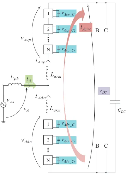
1 _C Aup v Aup v A i Aup i Adn i Ad n v DC v A v N 2 1 N 2 1 2 _C Aup v Cn Aup v _ 1 _C Adn v 2 _C Adn v Cn Adn v _ As v Acirc i arm L arm L ph L B C B C DC C
Fig. 1. MMC single phase representation.
The paper is organised as follows. The next section presents the MMC, basic equations and the organisation of the AC and DC side controllers. The following section discusses the pulsed DC load effects on the converter and the arm imbalances that occur to cause overmodulation with a corresponding effect on the AC side operation. Previously reported arm balancing methodologies are also discussed. The fourth section proposes the modified control algorithm to provide both arm balancing and low AC power fluctuation. The fifth and sixth sections validate the control algorithm by simulation and experiment, respectively.
II. MMC,EQUATIONS AND CONTROLLER
The three-phase MMC, represented in detail for phase A, is shown in Fig 1. The grid voltage, arm voltages (chain link voltages of upper and lower arm), phase current, arm currents, and fictitious circulating current are presented. Circulating current of phase A is calculated by (1).
iAcirc=
iAup+iAdn
2 (1)
The equivalent AC side equation is given by (2):
vAs−Leq
diA
dt +
vAup−vAdn
2 =
v++v−
2 ≈0 (2)
where v+
and v− are positive and negative DC voltage potentials, and Leq = Lph+ Larm
2 is equivalent AC circuit
inductance. ref AC P PI regulator A
i iB iC
ref A AC v _ ref B AC v _ ref C C A
v | _
ref d i ref q i
∑
= = = n k dn up jABC i Ck ij v .. 1 ,, ,_ PI regulatorS/H 20ms CALC
As
v vBsvCs
+
+
[image:2.612.312.565.67.244.2]A,B,C/d,q A,B,C/d,q
Fig. 2. AC side controller based on thed,qcurrent controller.
Voltage
regulator PI regulator 0.5 1/3 ref DC v DC v ref DC i Aup i Adn i ref A DC
v
_ + + ref Acirc i err Acirc i kcirc_pi circ k _ s
1 DC v ref A DC v _ + + ++
Fig. 3. DC side controller based on the circulating current controller.
Based on the AC side equation, the AC side controller is designed, by implementing a d, q current controller which produces the AC part of the reference, as presented in Fig. 2. The phase A AC side control variable, i.e. the AC part of the reference, is given by (3):
vAC A=−vAup−vAdn
2 ≈vAC A
ref (3)
The DC side equation used for the circulating current control is given by (4):
vAup+vAdn−2Larm
diAcirc
dt =v
+
−v−=vDC (4)
The circulating current controller (Fig. 3) is PI based and it compensates for the voltage drop on the two arm inductors, and together with the vDC as a feed-forward term produces
thevDC Aref:
vDC A=vAup+vAdn≈vDC Aref (5)
The circulating current reference is derived from the DC voltage controller that regulates the average DC voltage value to a constant reference. This reference can be corrected with a small DC component used for phase balancing, i.e. balancing of the capacitor voltages between the phases, as given in [7].
The normal modulation demands for the MMC converter are described by equation (6) for the upper and lower arm, respectively:
vAupref =
vDC Aref
2 −vAC A
ref
vAdnref =
vDC Aref
2 +vAC A
ref
(6)
The AC power fluctuation should be low, while the DC voltage should be controlled. To ensure this, the AC power is regulated via AC current control, while the DC voltage controller produces the DC current reference. The overall converter energy needs to be maintained, thus an energy controller is used to correct the input power reference (Fig. 2).
III. IMBALANCES CAUSED BY PULSEDDCLOAD
In the case of the MMC being used as a rectifier with resistive DC load, arm imbalances can occur as a consequence of transients and unbalanced arm inductances/cell capacitors which are present in a practical system. In the case of perfectly balanced converter arms, as is normal in simulations, the converter arms are naturally perfectly balanced, and there is no need for arm balancing controllers. However, in applications involving a pulsed DC load, arm balancing controllers are necessary to guarantee correct converter operation - even if the converter components and the supply are ideal.
Due to the klystron modulation repetition frequency, the DC voltage ripple has a 50Hz component. If a conventional controller/modulation is used, the DC voltage ripple will produce non-zero average power having opposite signs on the converter arms [7]. This causes divergence of the cell capacitor voltages of the two arms, even if the capacitor voltages within one arm are perfectly balanced. If the sum of capacitor voltages of one arm falls below the modulation signal, overmodulation occurs. As a consequence the overall arm voltage is distorted, leading to distortion of the converter phase voltage and current and an increased AC power distor-tion [7]. If the moduladistor-tion strategy follows (6), overmoduladistor-tion can be avoided by balancing the cell capacitors between two arms. To achieve that, the circulating current reference needs to have a 50Hz component [7]–[9]. For the specific application, the circulating current 50Hzcomponent should be shifted by
π
2 from the 50Hz component of the DC voltage ripple [7]
in order to create zero average power on both the upper and lower arms. Depending on the pulse position, i.e. the angle of the 50 Hz component in the DC voltage ripple, with respect to the AC voltage and current of a particular phase, different circulating current amplitudes should be used. The amplitude of the 50Hz circulating current component in a particular phase increases if the pulse position is such that it affects that phase more severely. The method in [7] balances the arm voltages for the majority of the pulse positions. However, due to the sensitivity to pulse position, there are pulse positions for which arm balancing is not possible. In an alternative solution, the 50Hz component of the circulating current can be aligned with the AC voltage reference [8], [9] and with a suitable amplitude, equal average power is achieved on the upper and lower arm. This provides arm balancing regardless of the pulse position but an additional phase balancing loop should be implemented (this loop is generally present to make sure equal power distribution among phases).
IV. PROPOSED MODULATION CHANGE
An alternative way to avoid overmodulation and ensure low AC power fluctuation is to redistribute the modulation signal in such a way that the AC part of the voltage reference and AC current are not distorted, i.e. that the equation (1) and (3) are satisfied. The distribution of the DC voltage reference should remain unchanged, to avoid zero sequence components in the converter AC voltages. The distribution of the AC part of the reference can be changed however. In that case the references for the upper and lower arm of phase A are given by following equations (7), instead of equation (6).
vAupref =vDC Aref −(1 +xA)vAC Aref
vAdnref =vDC Aref + (1−xA)vAC Aref
(7)
where xA is a parameter that describes redistribution of the
AC part of the reference between arms of phase A. In the steady state the parameterxis constant for all of the converter phases. This way, the AC voltage generated by converter is not affected and both AC and DC voltage references can be followed which would provide low AC power fluctuation.
The simplified converter diagram in the case of phase A is given in Fig. 4. From this schematic it can be seen that xAvAC A does not affect the AC side equivalent circuit
(common circuit, [10]), but only the DC side equivalent circuit (differential circuit, [10]). Thus, uneven distribution of the AC reference between two arms does not cause uneven distribution of the phase current between the two arms. However, the non-zero parameter xA causes appearance of a 50Hzcomponent
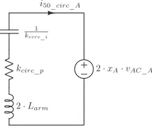
in the circulating current, acting as a disturbance for the circulating current controller which normally tries to maintain a constant reference. The equivalent DC side circuit (with focus on the 50Hzdisturbance) is presented in Fig. 5.
Since the circulating current now has a 50Hzcomponent, the circulating current controller will have non-zero error in steady state, with the mean value following the reference. Thus, the DC reference, comprised of the DC voltage feed-forward term and the PI controller output, is a function of the circulating current 50Hz component. Considering the circulating current PI controller parameters (Fig. 3) the DC voltage reference in the steady state can be approximated as:
vDC Aref =vDC+vDC A0
−kcirc p·iAcirc50 −kcirc i
Z t
0
iAcirc50(τ)dτ
(8)
Where vDC A0 ensures that the mean circulating current
follows its constant reference, and kcirc p and kcirc i are
parameters of the circulating current controller. From (8), and the DC equivalent circuit from Fig. 5, it can be concluded that the controller output can be modelled as a series connection of a resistor with the resistance ofkcirc p and capacitor with
+ −
+ −
+ −
+ −
+ −
+ −
vDC vAC A
iA
iAup
iAdn Larm
Larm Lph
vAs
xA·vAC A vDC A
2
vAC A
xA·vAC A vDC A
[image:4.612.398.507.44.136.2]2
Fig. 4. Simplified schematics of the phase A of an MMC with uneven distribution of AC voltage reference.
+
− − +
+ − + −
Larm iAcirc Larm
vDC CDC
vDC A 2
vDC A 2
!!"#$#% &'("#$#%
[image:4.612.93.249.49.293.2]xAvAC A xAvAC A
Fig. 5. Equivalent DC side circuit of phase A of an MMC with uneven AC reference distribution.
τcirc is the controller time constant) which at 50Hz
repre-sents a significantly higher impedance than the inductance (2Larmω) or capacitancekcirc i
ω . Thus, for a fast PI controller,
the impedance of the circuit from Fig. 6 is dominated by the real component. The resulting 50Hz component in the circulating current will be proportional to the AC voltage amplitude and the parameterxbut with the opposite sign and a small phase shift with respect to the AC voltage reference. Therefore, the operation of the method is related to the method from [8], [9].
The parameter x influences the average power difference between the upper and lower arm. Increasing xdecreases the arm power difference, which in turn causes a decrease in the difference between the upper and lower arm cell voltages. The benefit of this method is that it acts directly on the references to avoid overmodulation in the arms. Additionally, there is no need for explicit generation of a 50Hzcomponent in the circulating current references.
As shown in Fig. 7, the parameter xA is directly derived from the imbalance between the capacitor voltages of the upper and the lower arm, meaning that the arm with the lower
+ −
i50 circ A
2·Larm kcirc p
1
kcirci
2·xA·vAC A
Fig. 6. Circulating current 50Hzcomponent equivalent circuit in the case of uneven AC reference distribution, assuming PI based circulating current controller.
∑
= n k
Ck Aup
v n
.. 1
_
1
∑
= n kCk Adn
v n 1.. _
1
н
н н
Ͳ
PI regulatorS/H 20ms
й y
A x AVG
20ms
AVG 20ms
Fig. 7. ParameterxA generation on the basis of cell capacitor voltages on the example of phase A.
available voltage will have a lower amplitude of modulation signal. Even when imbalance is present, overmodulation is avoided by reducing the modulation amplitude of the arm with lower capacitor voltages. Using this approach further divergence of the voltages is halted and the voltages are re-balanced. The PI controller ensures zero steady state error and proper voltage balancing. The arm balancing controller from Fig. 7 is included in the overall control strategy, as presented in Fig. 8. This control strategy is particularly attractive for the application of interest where the power taken from the DC side is pulsed and the overall converter energy controller operates on the AC power reference. Also, the converter AC and DC sides are still decoupled meaning that low AC power fluctuation will be achieved despite the pulses on the DC side. From the AC phase voltage and DC voltage references, together with the parameter x, the arm modulation signal is formed (7) and normalised with the sum of the cell capacitor voltages of that arm. The number of cells to be inserted is used for modulation, where only one cell performs PWM within an arm. Selection of the cells involves sorting the capacitor voltages within each arm and using the arm current direction information [11].
!"#$%& #()&#*
+,-.%
#()&#* /&&%()
0!1#*)-2% #()&#*
!3&/*-)3(2
#()&#* /&&%() &4 5-*-(3(2
5-*-(3(2 +,-.% +#$%&
#&&%)3#(
!#$$%&' $%(%$%&%
)&*%$'+',-& ,&.,%*
#$$%&' $%(%$%&% !,$#/+',&0
1!2-/'+0% $%(%$%&% !2-/'+0% $%(%$%&%
1#*)-2%. !%**-"-3)#&
34,'5,&0 *,0&+/* 6#&4-*3.-)3#(
[image:4.612.326.548.187.234.2]7#8/*-)3#( -(8%** 5-*-(3(2 67+$+8%'%$
[image:4.612.63.286.334.411.2] [image:4.612.312.566.559.679.2]0 0.5 1 1.5 18
20 22
S
um
of t
he
a
rm
vol
ta
ge
s [kV
]
Upper arm Lower arm
0 0.5 1 1.5
−0.01 0 0.01 0.02 0.03
V
al
ue
of t
he
x
p
ara
m
et
er
Time [s]
0 0.5 1 1.5−2
−1 0 1 2
Im
b
al
anc
e
b
et
w
ee
n a
rm
s [kV
[image:5.612.72.277.52.220.2]]
Fig. 9. Phase A arm balancing: Top plot presents the sum of the cell capacitor voltages in the upper and lower arm; The lower plot presents the difference of the sum of the upper and lower arm cell capacitor voltages (averaged at 20ms), and the resultingxparameter.
V. SIMULATION RESULTS
[image:5.612.337.524.55.260.2]The MMC converter operating under pulsed load conditions, emulating klystron modulators, with the ratings given by Table I, has been simulated in the PLECS environment. The sampling frequency and equivalent switching frequency is 10kHz. The relevant controller gain values, are given in the Table II for the d,qand circulating current controller and for the arm balancing controller.
TABLE II CONTROLLER GAINS.
Controller Proportional Integral
Phase currents kdq p 9 kdq i 900
Circulating currents kcirc p 13.5 kcirc i 540
Arm balancing kx p 0.3 kx i 1
The following results relate to the pulse occurring 1.67ms after the grid voltage phase A positive zero crossing which corresponds to a pulse position of 0.524rad. Fig. 9 illustrates the phase A arm balancing principle applying the proposed method. The upper plot shows the sum of the cell capacitor voltages in the upper and lower converter arm, and illustrates their convergence. The reasons for the imbalance between the arms in this case are both the transient (the simulation starts at zero power transmission and ends at 16MW) and the pulsed-load effects. The lower plot presents the arm balancing con-troller waveforms (Fig. 7). Based on the normalised difference between the sum of the capacitor voltages in the upper and lower arm (i.e. the error) the PI controller generates a suitable value of the xA parameter. If the source of imbalance was only the transient, as it is in the case of a resistive load, the steady state value of the parameter xA would be zero. Here,
the steady state value of xA is a measure of how much the
pulsed load affects phase A.
Fig. 10 presents the converter waveforms in the steady state. The converter phase A voltage and current are presented on
1 1.02 1.04 1.06 1.08 1.1
−10 0 10
P
ha
se
A
vol
ta
ge
[kV
]
1 1.02 1.04 1.06 1.08 1.1
−2000 0 2000
P
ha
se
A
c
urre
nt
[A
]
1 1.02 1.04 1.06 1.08 1.1
18 20 22
D
C vol
ta
ge
[kV
]
1 1.02 1.04 1.06 1.08 1.1
700 800 900
D
C c
urre
nt
[A
]
Time [s]
Fig. 10. Converter waveforms vs. time: Phase A voltage (towards grid neutral), phase A current, DC voltage and DC current.
1 1.02 1.04 1.06 1.08 1.1
−500 0 500 1000
Time [s]
P
ha
se
A
c
urre
nt
s [A
]
Upper arm Lower arm Circulating current
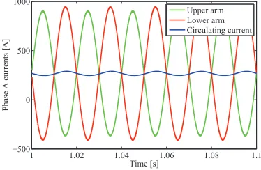
Fig. 11. Phase A arm currents and circulating currents vs. time.
the top two plots, while the DC voltage and the DC current are presented in the two lower plots. During the pulse the one sample delay present in the DC voltage reading, which is used as a feed-forward term in the circulating current controller, causes a spike in the DC and circulating currents. Here, a one sample delay compensation is applied on the DC voltage reading for the sampling instants during the pulse (with 10kHz switching frequency those are one or two samples), so the spike in the DC current is almost negligible. Despite that, the 50Hz component is present in the DC current, as a consequence of the 50Hz component in the circulating currents. The amplitude of the DC current ripple does not vary much with the pulse position, but its phase shift does. Fig. 11 presents the phase A arm currents and circulating current. The arm currents have different amplitudes of the 50Hz component due to the presence of the fundamental in the circulating current that is almost in phase opposition with the converter phase A voltage (refer to the Fig. 10). Fig. 12 shows the converter AC and DC side power. It can be seen that the AC power ripple is very low, below 0.3%.
[image:5.612.338.525.312.434.2]1 1.02 1.04 1.06 1.08 1.1 15.98
16 16.02 16.04
A
C
p
ow
er [M
W
]
1 1.02 1.04 1.06 1.08 1.1
14 16 18
D
C
p
ow
er [M
W
]
[image:6.612.331.523.58.211.2]Time [s]
Fig. 12. Converter AC and DC side power vs. time.
0 0.5 1 1.5 2
0.22 0.23 0.24 0.25 0.26 0.27 0.28
A
C
p
ow
er fl
uc
tua
ti
on [%]
Pulse position [rad] 0 0.5 1 1.5 2
18.1 18.2 18.3 18.4 18.5 18.6
D
C
p
ow
er fl
uc
tua
ti
on [%]
Pulse position [rad]
Fig. 13. AC and DC power fluctuation vs. the pulse position obtained by simulation.
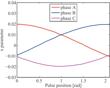
respect to the phase A grid voltage zero crossing, covering one third of the grid period. The AC power fluctuation (Fig. 13) is around 0.25% for all pulse positions, which means the performance of the method is insensitive to the pulse position. The DC power fluctuation (Fig.13) is around 18.5%, which is increased when compared to the nominal 10% created by the DC voltage droop. Fig. 14 presents the steady state value of the parameter x for different pulse positions. From the simulation results the values of parameter xA,B,C are below
2%, meaning that this small redistribution of the modulation signals is enough for achieving arm balancing in the case of 10%DC voltage droop. It can be seen that pulses positioned at the zero crossing of phase A affect the powers in that phase most significantly (the highest value ofx) and this relationship is the same in the other phases.
VI. EXPERIMENTAL RESULTS
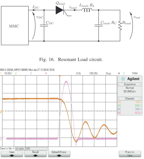
A small scale prototype has been built for the purpose of validating the behaviour of the grid connected MMC under pulsed DC load conditions. The 4 cell per arm, 7kWconverter has been designed by scaling down both the converter voltages and currents with the same scaling factor. A photograph of the experimental converter is presented in Fig. 15. A resonant circuit is used to emulate the pulsed DC load, this generates a 3.2kA current pulse in a shape of half a sinusoidal (Fig. 16) when it is triggered. Table III lists the converter and the load parameters. The load parameters are designed to provide the same average current (16.5A) as the scaled flat top pulse in the real application (same pulse area and duration). This results in ≈π2 times higher peak pulse current.
0 0.5 1 1.5 2
−0.03 −0.02 −0.01 0 0.01 0.02 0.03 0.04
x
p
ara
m
et
er
[image:6.612.324.542.79.556.2]Pulse position [rad] phase A phase B phase C
[image:6.612.56.287.213.312.2]Fig. 14. Phase A, B and Cxparameter values vs. the pulse position obtained by simulation.
Fig. 15. Three phase MMC with 4 cells per arm.
TABLE III
EXPERIMENTAL CONVERTER AND LOAD PARAMETERS.
Description value
Rated power 7kW
DC voltage 400V
AC voltage 225V
Number of cells per arm 4 Nominal cell voltage 100V
Phase inductance 3mH
Arm inductance 1.5mH
Cell capacitance 3.3mF
DC link capacitance 8.5mF
DC voltage droop 40kV
Pulse frequency 50Hz
Pulse duration ≈150µs
The control algorithm is realised in a DSP-FPGA plat-form, including a Texas instruments 225MHz TMS320C6713 DSP and FPGA cards used for data acquisition and PWM signal generation. The DSP board is equipped with the DSK6XXXHPI daughter card used for downloading the code and online monitoring of the control variables through the Matlab host interface. The waveforms captured through the host interface are sampled at 10kH, which is the DSP sam-pling frequency and thus they often have reduced switching ripple. Some of the results presented here are based on the host interface data. Other waveforms are captured with a 200MHz oscilloscope.
[image:6.612.321.552.248.353.2] [image:6.612.346.520.378.552.2]!
CDC Cload, RC Rload
Lload, RL
Qload
iload
IDC
[image:7.612.57.295.51.315.2]vDC vout
Fig. 16. Resonant Load circuit.
Fig. 17. Load current pulse (pink, 500A/div) shaped with the resonant circuit and the DC voltage ripple (yellow, 10V/div) vs. time (100µs/div).
the current pulse and the droop of the DC voltage. The current pulse is nearly 3.2kA while the voltage droop is about 45V (around 10%) and the nominal DC voltage is 400V.
Figures 18, 19 and 20 are captured for a pulse occurring 1.7ms after the phase A grid voltage positive zero crossing, corresponding to a pulse position of 0.534rad. Fig. 18 presents a converter waveforms under pulsed load conditions. Here the phase A converter voltage and current are presented together with the DC voltage and current. The DC voltage has about 10%voltage droop. Fig. 19 presents the converter/grid phase currents and the DC voltage with the pulsed DC load. As shown, there is no noticeable distortion in the AC currents, thus, as desired, the pulsed load effects are not propagated to the AC grid. Fig. 20 shows the effectiveness of the arm balancing algorithm based on the sum voltages of the upper and lower arm of phase A.
The AC and DC power fluctuations vs. the pulse position (computed on the basis of the host interface obtained AC voltages and currents and the DC voltage and current) are presented in Fig. 21. The values obtained are expected to be lower than the true values since the current switching ripple is rejected by the host interface sampling effect.
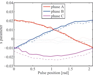
Similarly, the values of the xA,B,C parameter for phases
[image:7.612.318.557.51.202.2]A, B and C vs. the pulse position are presented in Fig. 22. Here, the dotted lines represent the internal imbalance present between the arms (in no load condition) which is dependent on the sensor calibration, temperature and imbalance between cells and arms. The imbalance is not significantly dependant on the rated power, meaning that its influence on the power imbalance and x parameter values is similar at full power,
Fig. 18. Nine-level phase A converter voltage with respect to the grid neutral (yellow, 100V/div), phase A converter/grid current (green, 10A/div), converter DC voltage (blue, 100V/div) and converter DC current (magenta,
10A/div) vs. time (5ms/div).
Fig. 19. Converter DC voltage (yellow, 100V/div), converter/grid currents: phase A (green, 10A/div), phase B (blue, 10A/div) and phase C (magenta,
10A/div) vs. time (2ms/div).
but it is dependant on the temperature. The dashed lines represent the values of x parameter recorded during pulsed load conditions for different pulse positions. The full lines are the difference between the x parameters values during pulse and before pulse and they are associated with the pulsed-load effects. It can be seen that the experimental results are in agreement with the simulation results.
VII. CONCLUSION
0 0.02 0.04 0.06 0.08 0.1 380
390 400 410 420 430
V
ol
ta
ge
s [V
]
Time [s]
[image:8.612.332.523.57.211.2]Upper arm sum Lower arm sum DC voltage
Fig. 20. Sum of the phase A upper and lower arm capacitors voltages and converter DC voltage vs time obtained by the host interface.
0 0.5 1 1.5 2
1.3 1.4 1.5 1.6 1.7 1.8
A
C
p
ow
er fl
uc
tua
ti
on [%]
Pulse position [rad] 0 0.5 1 1.5 2
22 24 26 28 30
D
C
p
ow
er fl
uc
tua
ti
on [%]
Pulse position [rad]
Fig. 21. AC and DC power fluctuation vs. the pulse position obtained by the host interface.
is a measure of redistribution of the AC reference between converter arms, is below 2% for all pulse positions.
A small scale prototype was developed to experimentally prove the proposed approach. The arm balancing algorithm has proven successful, leading to undistorted grid currents. Exper-imentally, the AC and DC power fluctuations are higher when compared to the simulation results, but the MMC used has lower number of levels, and the emulated load does not draw flat-top pulses. The measured AC power fluctuation is below 2%. The values of thexparameter have the same dependence on the pulse positions as those obtained by simulation.
Additionally a certain amount of imbalance between the arms was present in the no-load and resistive load operation. This is probably caused by the unsymmetrical (non-ideal) converter cells and arm inductances in the real converter, and also in the transducers that are used for sensing the capacitor voltages and arm currents. All those sources of imbalance are temperature dependent. The proposed method inherently copes with those imbalances in addition to those created by the pulsed load. Therefore, the proposed method could be used for different applications of the MMC other than that considered here.
The proposed algorithm does not explicitly impose a 50Hz harmonic in the circulating current but this comes as a conse-quence of the AC reference redistribution and it has a phase shift with respect to the AC voltage reference of nearly 180◦ degrees in the case of a positive value ofx(0◦degrees in the case of a negative value ofx). Therefore the method generates similar circulating currents to the method reported in [8], [9] but with decreased control complexity.
0 0.5 1 1.5 2
−0.03 −0.02 −0.01 0 0.01 0.02 0.03 0.04
x
p
ara
m
et
er
[image:8.612.63.280.57.173.2]Pulse position [rad] phase A phase B phase C
Fig. 22. Phase A, B and Cxparameter values vs. the pulse position obtained by the host interface.
ACKNOWLEDGMENT
This project has been founded and it is a part of a collab-oration with the European Organization for Nuclear Research (CERN).
REFERENCES
[1] A. Lesnicar, and R. Marquardt,An innovative modular multilevel con-verter topology suitable for a wide power range, inPower Tech Confer-ence Proceedings, Bologna, Italy, CD-ROM paper, 2003.
[2] D. Aguglia, C. Martins, M. Bastos, D. Nisbet, D. Siemaszko, E. Sklavounou, and P. Viarouge,Klystron modulator technology challenges for the compact linear collider (clic), in Proc. of IEEEPulsed Power Conference (PPC), Chicago, USA, pp. 1413-1421, 2011.
[3] M. Jankovic, A. Watson, J. Clare, P. Wheeler, and D. Aguglia, Grid Interface Design for the Compact Linear Collider (CLIC), in Proc. of
Power Electronics and Applications (EPE), Geneva, Switzerland, CD-ROM paper, 2015.
[4] M. Zygmanowski, B. Grzesik, and R. Nalepa,Capacitance and induc-tance selection of the modular multilevel converter, in Proc. ofPower Electronics and Applications (EPE), Lille, France, CD-ROM paper, 2013. [5] F. C. Magallanes, D. Aguglia, P. Viarouge, C. de Almeida Martins, and J. Cros, Design of a Solid-State Fast Voltage Compensator for klystron modulators requiring constant AC power consumption, in Proc. ofInternational Power Modulator High Voltage Conference - IPMHVC 2014, Santa Fe, USA, CD-ROM paper, 2014.
[6] M. Hagiwara and H. Akagi, Control and Experiment of Pulsewidth-Modulated Modular Multilevel Converters, in IEEE Trans. on Power Electronics, vol. 24, pp. 1737-1746, 2009.
[7] M. Jankovic, A. Costabeber, A. Watson and J. Clare,Control of a Grid Connected Modular Multilevel Converter under Pulsed DC Load, in Proc. of IEEEIndustrial Electronics Society Conference (IECON), Yokohama, Japan, CD-ROM, 2015.
[8] J. Pou, S. Ceballos, G. Konstantinou, V. G. Agelidis, R. Picas and J. Zaragoza,Circulating Current Injection Methods Based on Instantaneous Information for the Modular Multilevel Converter, in IEEE Trans. on
Industrial Electronics, vol. 62, pp. 777-788, 2014.
[9] S. Fan, K. Zhang, J. Xiong, and Y. Xue,An improved control system for modular multilevel converters with new modulation strategy and voltage balancing control, in IEEE Transactions onPower Electronics, vol. 30, pp. 358371, Jan 2015.
[10] J. Pou, S. Ceballos, G. Konstantinou, G. J. Capella and V. G. Agelidis,
Control strategy to balance operation of parallel connected legs of modular multilevel converters, in Proc. of International Symposium on
[image:8.612.58.288.218.313.2]