Simultaneous Wireless Information and GaN-based
Power Transfer Exploiting a Dual Frequency Band
J. Maximilian Placzek,
Peter A. Hoeher,
Fellow, IEEE
Chair of Information and Coding Theory Kiel University, 24143 Kiel, Germany
{jmpl,ph}@tf.uni-kiel.de
Pramod K. Prasobhu
+,
Student Member, IEEE
,
Marco Liserre
+,
Fellow, IEEE
,
Giampaolo Buticchi*,
Senior Member, IEEE
+Chair of Power Electronics
Kiel University, 24143 Kiel, Germany
+{pkp,ml}@tf.uni-kiel.de
*PEMC Group,University of Nottingham Ningbo China, 315100 Ningbo, China
Abstract—A simultaneous wireless information and power transfer system employing separated frequency bands for energy and data, dubbed dual-band SWIPT, is investigated. Elementary circuit elements are optimized numerically. An experimental testbed based on a gallium nitride (GaN) full-bridge converter demonstrates data rates in excess of 450 kbps employing on-off keying in conjunction with a simple diode detector for data recovery.
Index Terms—Inductive power transmission, Data commu-nication, Inductive charging, Frequency division multiplexing, SWIPT
I. INTRODUCTION
In many applications, wireless power transfer should be coupled with data transfer - for example as a means of closed loop control of the power transfer. An elegant solution is dubbed simultaneous wireless information and power transfer (SWIPT), using a single set of coils for both functions. [1], [2]. Possible applications include medical implants and (semi)autonomous underwater apparatus, as neither plug in power/data connections nor conventional wireless communi-cations are particularly satisfactory in such environments.
The simplest implementation of this approach is single-band SWIPT – data transfer by modulation of the power transfer. While useful for small power levels, its practicality is limited for high power levels at high efficiency. Modulation represents a random perturbation of the power transfer, disrupting optimal switching conditions and controlled operation. Furthermore, optimization of the passive components for efficient power transfer typically leads to low bandwidth and suboptimal communication. In the communications literature, fundamental information-theoretical bounds have been derived concerning the trade-off between efficiency and data rate [3]. Possible switching techniques between power and data rate have been investigated in-depth [4], [5].
This work was supported in part by the European Union/Interreg V-A - Germany-Denmark, under the PE:Region Project and in part by the European Research Council under the European Unions Seventh Framework Programme (FP/2007-2013)/ERC Grant 616344-HEART and in part by the Ningbo Science & Technology Bureau under Grant 2013A31012 and NSFC under Grant 51650110507
In order to resolve the conflicting demands with respect to bandwidth, frequency-division multiplexing (FDM) is a possible solution. FDM techniques can be realized in quite different forms. In [6], two coils are operated in parallel. Energy is transmitted via the so-called power coil, data via the so-called information coil. In the dual-band SWIPT system investigated in [7], an additional LC circuit is inserted at the primary side as well as at the secondary side. One of these additional LC circuits is employed for data transmission, the other one for data pick-up. Therefore, duplex communication is feasible. Upon properly designing the overall network, the power transfer efficiency will not significantly be decreased by the communication unit and, vice versa crosstalk will be suppressed, i.e. data communication will be reliable.
In this contribution, the dual-band SWIPT system inves-tigated in [7] will be taken as a baseline system. However, several modifications are performed to yield improved per-formance: (i) The series-parallel topology favored in [7] is replaced by the series-series topology. That way, efficiency is improved when the effective load resistance is small. Also, a voltage transfer ratio close to one can be achieved for many parameter sets. (ii) In [7], a target data rate of about 20 kbps has been achieved, which is fast enough for the control loop. In this contribution, however, a design goal is to maximize data rate given a high power efficiency. Towards these goals, all circuit components are numerically optimized. We could achieve data rates of 450 kbps and beyond without using a complicated data equalizer or compromising power transfer. (iii) Last but not least, we attempted to utilize GaN HEMTs in an ongoing effort to exceed Si MOSFET performance. Besides computer-based component optimization, experimental results have been obtained.
II. SYSTEMOVERVIEW
A. Power Transfer
stage in the secondary side performs the final conversion stage and feeds the battery/load. The most adopted solution for coil excitation is to use a power electronics converter to generate a voltage square wave on the primary coil [8]. Although capacitors may be used for compensation, some authors propose more complex matching networks to improve transmission gain over wider coupling range [9].
Fig. 1: Basic schematic of a wireless power transfer system.
We choose the series-series topology as the most common and practical approach from literature.
The voltage gain depends on the distance of the coils, hence the coupling factor, the effective load resistance, and the operating frequency. Having primary converter control with near resonant frequency operation for regulation can lead to lower efficiency despite reduced number of processing stages [10]. To add another degree of freedom, voltage can be controlled via a primary and/or secondary DC/DC converter or specialized modulation schemes of the main DC/AC converter, i.e. asymmetric PWM, enabling resonant switching in one leg while using the other for modulation.
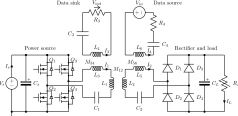
The schematic topology of the overall system under inves-tigation is shown in Fig. 2. At the primary side, a full-bridge DC-AC converter is implemented. Voltage and inner resistance of the source are denoted as Vs and Rs. The power source
drives a series circuitC1,L1. This circuit is in resonance with
the series circuitC2,L2 on the secondary side. The coupling
coefficient is defined as k12=M12/√L1L2, whereM12 is the
mutual inductance between the power coils L1andL2.
Com-pensation is performed such that f1=1/(2πp(L1+L3)C1) =
1/(2πp(L2+L5)C2) is the resonant frequency for power
transfer (neglecting bifurcation), whereL3L1andL5L2.
The ac resistances of L1 and L2 are denoted as R1 and R2,
respectively. At the power pick-up side, a full-bridge rectifier is implemented. The load resistance RL is varied in order to
emulate different output powers, charging states, and battery types.
Q1
Q2
Q3
Q4 +
− Vs
Is
+
Cs
L3
I1
L1
C1
L2
L5
I2 D 1
RL
IL
D2 D4
D3
+
CL
C2 + − Vin
L6 I 4
C4
R4
R3
C3
L4 I 3
Vout
M12
M34 M56
Data source Data sink
[image:2.612.54.292.566.682.2]Rectifier and load Power source
Fig. 2: Topology of the overall system under investigation.
B. Data Transfer
As suggested in [7], transformers consisting of coils L3,L4
and L5,L6, respectively, are inserted into the main loop for
the purpose of data transmission, subsequently dubbed data coils. The ratios L3/L4 and L5/L6 are proportional to the
turns ratio, which is assumed to be one. The corresponding mutual inductances are denoted asM34andM56, consequently
k34=M34/√L3L4 andk56=M56/√L5L6. Both transformers
are part of LRC networks L4,R3,C3 and L6,R4,C4,
respec-tively. The resonant frequency of these networks is f2 =
1/(2πpL40C3) =1/(2π
p
L06C4), where L04 is an equivalent
inductance approximated as 1/L04≈1/L4+1/L1≈1/L4.
Sim-ilarly, 1/L06≈1/L6+1/L2≈1/L6. The resonant frequency f2
should be at least about one decade higher than the resonant frequency f1for power transfer in order to suppress crosstalk.
The voltage of the data source is calledVin. Obviously there
is a trade-off between power efficiency and data reliability, which can be controlled by the ratio Vs/Vin. Resistor R4 is
subject for optimization. It includes the inner resistance of the data source and the ac resistance of L6. The data output
is the voltage drop across resistor R3, which includes the ac
resistance of L4. Resistor R3 is subject for optimization as
well, along with all capacitors and inductors addressed so far. Since our main concern is on data transmission via the return link, the Tx unit (data source) is inserted at the secondary side, whereas the Rx unit (data sink, data pick-up) is inserted at the primary side. However, system analysis does not change when Tx and Rx unit would be exchanged, providing that the two frequency bands are sufficiently splitted. Even full duplex communication is feasible. For symmetry reasons, we assume a series circuit in both data loops, whereas in [7] a parallel circuit has been taken at the Rx unit.
III. SYSTEMANALYSIS
Tasks and constraints of system optimization are manifold:
• Of primary concern is to maximize efficiencyηof power transfer.
• Simultaneously, data rate should be optimized. Since data rate depends on many parameters, including bandwidth, signal-to-noise ratio, modulation scheme, data detection, equalization, channel estimation and so forth, focus will be here on maximizing the channel capacity. Channel capacity is the maximum data rate at which information can be transmitted virtually error free.
• Finally, the power transfer efficiency shall not signifi-cantly be decreased by the communication unit and, vice versa crosstalk shall be suppressed, i.e. data communica-tion shall be reliable.
The free parameters to be optimized includeC1. . .C4,L1. . .L6
andR3,R4, as well as voltagesVsandVin. In order to obtain an
overall optimization at reasonable computational complexity, we propose to start with a maximization ofη=P2/P1given
in-active data loops (R3=R4→∞,Pdata=0), and to freeze these
A. Kirchhoff ’s Circuit Laws
The overall system can completely be expressed by Kirch-hoff circuit laws
VRs(s) +VL3(s) +VC1(s) +VR1(s) +VL1(s) = Vs(s) −VL2(s) +VR2(s) +VC2(s) +VL5(s) +VRL(s) = 0
VC3(s) +VL4(s)−Vout(s) =0
VR4(s) +VC4(s) +VL6(s) =Vin(s) −VL1(s) +sL1I1(s)−sM12I2(s) =0 −VL2(s)−sL2I2(s) +sM12I1(s) =0 −VL3(s) +sL3I1(s) +sM34I3(s) =0 −VL4(s) +sL4I3(s) +sM34I1(s) =0 −VL5(s) +sL5I2(s) +sM56I4(s) =0
−VL6(s) +sL6I4(s) +sM56I2(s) =0 (1)
together with ten component laws of the form
−VRi(s) +Ii(s)Ri = 0
−VCi(s) +Ii(s)/(sCi) = 0. (2)
These equations can be expressed in vector/matrix form as:
A·x=b (3)
Consequently, the unknowns inx are obtained as
x=A−1·b. (4)
Frequency splitting [11], also called bifurcation, is inherently included in the formulas at short distances between the power coils.
B. Results for Power Transfer Unit
In the prototype under investigation, power coils with an inductance of L1=L2=16.8 µH are used. The ac
resis-tance of R1 and R2 is experimentally obtained as R1(f) =
R2(f) ≈RDC(1+9.42·10−10· f2) with RDC =12.7 mΩ.
This approximation is quite tight for frequencies up to about 150 kHz.L3=L4is initially chosen to be 0.1L1(and optimized
subsequently). All these parameters are fixed throughout the optimization of the power transfer unit.
AssumingVL=24 V without loss of generality, the effective
load resistance isRL=5.76Ω, 2.88Ω, 1.152Ω, and 0.576Ω
at an output power of 100 W, 200 W, 500 W, and 1 kW, respectively. As a default number, P2=200 W (i.e., RL=
2.88Ω) is taken.
For symmetry reasons, in numerical results we assumeC1=
C2sinceL1=L2. In that case optimization simplifies forL3=
L4=L5=L6andC3=C4. The default coupling coefficient of
the power loop is k12=0.5, which corresponds to a distance
of about 3 cm.
In order to reduce the number of parameters when op-timizing the efficiency of the power loop, η=P2/P1, the
data loops are deactivated. Towards this goal, R3=R4→∞.
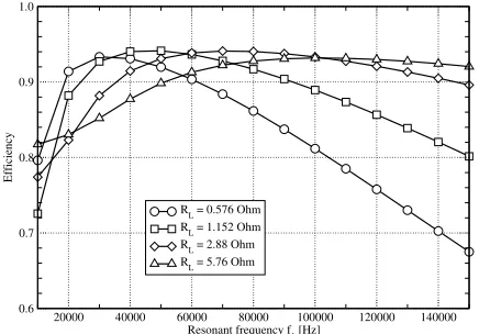
The remaining parameters are RL and k12, if η is plotted versus resonant frequency f1. C1 =C2 are determined as
20000 40000 60000 80000 100000 120000 140000
Resonant frequency f1 [Hz] 0.6
0.7 0.8 0.9 1.0
Efficiency
RL = 0.576 Ohm RL = 1.152 Ohm RL = 2.88 Ohm RL = 5.76 Ohm
Fig. 3: Efficiency as a function of resonant frequency f1given
coupling coefficientk12=0.5.
C1=1/[(L1+L3)·(2πf1)2], where f1 is changed between
10 kHz and 150 kHz.
As shown in Fig. 3, the resonant frequency should be carefully selected in order to maximize efficiency. At RL=
2.88Ω, the optimum frequency is f1≈70 kHz. Upon
reduc-ing/increasing RL, the optimum f1 reduces/increases. When
reducing/increasing the coupling coefficientk12, f1should be
increased/decreased. Subsequently, f1is fixed to be 70 kHz at
default parametersRL=2.88Ωandk12=0.5. When activating
both data loops, the same optima are obtained as long as f2f1 andVin/Vs is reasonably small. In other words: The
data loops do not affect the optimization of the resonant frequency of power transfer.
C. Results for Data Transfer Unit
Since a periodic square-wave source signal vs(t)generates
harmonics at odd multiples of f1 and causes minima at even
multiples of f1, a favorite design rule is
f2=2n·f1, (5)
wherenis a positive integer number.
Let us divide the frequency range into frequency bins of bandwidth ∆B each. Channel capacity of the data unit is
defined as [12]
C= lim ∆B→0
∆B
2
∑
i log2(1+SNRi), (6)where SNRi=Pi/Ni is the signal/noise ratio of the ith
fre-quency bin. In the system under investigation, the lowest frequency bin is determined by f1 (because of the crosstalk
constraint f2>10f1), whereas the largest frequency bin is
determined by the self resonance of the power coil. In order to get rid of such a fussy definition, in our numerical results we take only those frequency bins into account that are subject toSNRi≥1, since practical receiver implementations typically
fail at SNR levels below about 0 dB. Channel capacity natu-rally increases with increasing resonant frequency f2, because
then more bandwidth is available. For that reason, f2 should
[image:3.612.329.547.50.202.2]0.0 0.5 1.0 1.5 2.0 Inductance L3 [uH]
0 100000 200000 300000 400000 500000
Channel capacity [bit/s]
[image:4.612.62.290.51.202.2]Vin = 5 V, Vs = 24 V Vin = 7 V, V = 24 V
Fig. 4: Channel capacity as a function of L3given the default
parameters under investigation.
about 6.1 MHz for the power coils used in the prototype, the region up to 4.5 MHz is best suitable for f2. Therefore, we
select f2=4.48 MHz=64f1.
Channel capacity is found to be independent ofR3. Without
loss of generality, we choose R3=10 Ω. With increasing
R3, current I3 reduces, but noise is likely to become more
dominant.
Channel capacity monotonically improves with decreasing resistanceR4. There is a trade-off between the quality factorQ
and the length of the impulse response. We select R4=1 Ω,
because for R4<1 Ω the impulse response would be very long.
Since f1, f2, and all parameters of the power loop are
already optimized, and since R3 and R4 are not relevant
with respect to maximizing channel capacity, the remaining parameter subject for investigation isL3=L4=L5=L6. Signal
power Pi=Re{Vout,i·Vout∗ ,i/R3} at the data sink is obtained
by solving Eq. (4) given Vs=0 and Vin>0. Vice versa,
noise power Ni =Re{Vout, i·Vout∗ ,i/R3} at the data sink is
obtained by solving Eq. (4) given Vs>0 andVin=0. Thus,
comparatively the power transfer unit is the dominant noise source.
The noise power is a function of the power spectral density of the power converter. Ideally, the power converter outputs a square-wave signal in time domain with periodT =1/f1and
amplitudeVs. The corresponding Laplace transform is
Vs(s) =
Vs
s tanh(s T/4) = Vs
s
1−es T/2
1+e−s T/2, (7)
which corresponds to a line spectrum. Consequently, channel capacity is unrealistically high when the resonant frequencies are based on design rule (5). As an alternative, one may assume Vs(s) =Vs for all frequencies. This case establishes
the worst power spectral density. The channel capacity results reported next are based on this worst case.
As depicted in Fig. 4, channel capacity is optimized at L3=L4=1.4 µH for the default parameters under
investi-gation. This value is less than 0.1L1 and hence acceptable.
The corresponding compensation capacitors are yielded as
C3=C4≈1/(L04(2πf2)2≈0.98 nF. The optimal value of L3
is independent of the ratioVin/Vs.
Channel capacity is boosted withVin, at the cost of effective
efficiency ηe f f =P2/(P1+Pdata). Given Vs =24 V (about
200 W @ 2.88 Ω),Vin=5 V is sufficient for reliable data
detection. AtVin=5 V, the impact of the data unit onto the
power waveform is negligible. In the simplest case, data can be transmitted by on-off keying, i.e.,Vinis switched on or off.
IV. PRACTICALDESIGNCONSIDERATIONS
A. Power Transfer
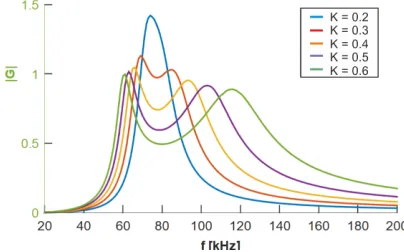
In case of WPT systems for EV charging, the battery charger equivalent resistance varies over a particular range. The characteristic resonant frequency shifts with varying charging port/coil distances. Accordingly, the converter op-erating frequency needs to be modified if the system has to be operated at optimal efficiency. Operation close to the resonant frequency minimizes reactive power and increases efficiency. In this implementation the devices are operated to achieve ZVS, hence at a frequency slightly higher than the resonant frequency. The efficiency peaks at the resonant point increases with larger coupling factors. Although the efficiency increases with the coupling factor, the gain plot in Fig. 5 shows that the achievable gain reduces at higher coupling. Hence a small trade-off with regard to the reactive power flow and desired gain needs to be considered as well.
Fig. 5: Gain plots vs frequency of the wireless transfer system for variousk values viz - 0.2, 0.3, 0.4, 0.5, 0.6 .
Thus for a particular battery charger system, the design critical criteria are that the system should be capable of transferring the nominal power at the highest possible coupling factor (here selected as k=0.6) even at the lowest load resistance.
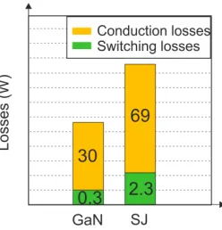
Using wideband gap devices like GaN further enables a highly efficient power conversion compared to Si-based solutions. This is attributed to their smaller output capacitances Cossand lower drain source resistance valuesRds,onfor similar
blocking voltages and currents compared to Si MOSFETs which results in lower losses as shown in Fig. 6.
[image:4.612.335.537.385.511.2]Fig. 6: Loss comparison of GaN HEMT vs Si-based Super Junction (SJ) MOSFET (GS66504B vs IPW65R190CFD).
• A smaller value ofkleads to a steep gain curve and hence the frequency range required to regulate converter voltage is kept small. This however causes higher circulating current. As a result, the conduction losses rise.
• A higher value of k would result in a flatter curve and therefore the required frequency range to regulate the output voltage is higher. However, a higher value reduces the circulating current.
• The available magnetizing inductance has also an impact on the dead time. By increasing the magnetizing induc-tance, the magnetizing current is decreased and the dead time needs to be increased.
B. Data Transfer
The numerical model of the circuit describes the data coupling transformers as ideal transformers. To approximate this behavior in reality, a high coupling factor has to be achieved. Instead of utilizing conventional ferrite transformers [7], the low inductance value resulting from optimization allows the use of air-cored transformers which achieve high coupling through bifilar interlacing of separate litz conductors. The default coupling coefficient of the air-core transformers is about k34=k56=0.9 according to practical experience. For
testing purposes, the data signal source Vin is realized as a
half-bridge circuit, employing two switches and a capacitive voltage divider. A diode-based envelope detector is chosen as receiver. A pseudo-random binary sequence modulates a square wave with the fundamental frequency f2 via on-off
keying, which in turn controls the half-bridge. This setup demonstrates bandwidth, signal quality, and the possibility of processing high data rates with simple circuitry. It is, however, not necessarily the communications topology of choice for this application, a variety of modulation schemes and transceivers are viable. In this regard, the notion of signal-to-noise ratio (SNR) deserves further discussion. While the data signal is subject to relevant interference from the harmonics of the power transfer, this crosstalk is a periodic, causal, and easily predictable signal and therefore by definition not true noise. It can be compensated for by adaptive filtering, or circum-vented by methods such as discrete multitone transmission (DMT) in conjunction with adaptive bit loading in order to
approach Eq. (6). Adaptive bit loading implies that ”noisy” subcarriers are deactivated. Similar reasoning applies to the channel impulse response. It is possible to reduce intersymbol interference by equalization.
V. EXPERIMENTALRESULTS
A proof of concept of the proposed SWIPT system is realized with an experimental test-bed featuring numerically optimized passive circuit components and GaN semiconduc-tors for the power electronics part.
A. Description of Setup and Design Parameters
The DC/DC converter implemented here is a GaN-based full-bridge with GaNSystems GS66504B on primary side driven by Silabs gate drivers controlled by microcontroller MPC5643L. The magnetic coupling system consists of litz wires and radial ferrite cores arranged behind the flat coils to improve coupling and copper utilization. The diameter of this arrangement as shown in Fig. 8 is 23 cm. The secondary consist of MBRS10100 Si Schottky diodes in a full bridge rectifier configuration. All tests have been carried out with this configuration. The communication coupling transformers consisting of L3/L4 and L5/L6 are wound with 4 turns of a
bifilar arrangement of the same litz wire used for the power coils interlaced with an additional thin conductor. Communica-tion is driven by an IXDN630 monolithically integrated high speed half-bridge and a capacitive voltage divider, resulting in a square-wave input amplitude Vin to the communication
system of half the auxiliary supply voltageVdd. Data symbols
[image:5.612.311.563.476.537.2]are generated and received by an Analog Discovery 2 (AD), 100 Mbps digital signal generator and oscilloscope system. The envelope detection circuit is constructed according to Fig. 7.
Fig. 7: Envelope detector connected to the SWIPT system.
Actual circuit parameters are tabulated as:
Power System Comm. System
Vs 15 V Vdd 12 V
L1/2 16.8 µH L3/4/5/6 1.2µH
C1/2 280 nF C3/4 1 nF RL 2.88Ω R3,R4 10Ω, 1 Ω
f1 70 kHz f2 3.68 MHz
The measured value of f2=3.68 MHz deviates from the
B. Experimental Setup and Waveforms
[image:6.612.342.534.52.205.2]The converter system based on the above description is shown in Fig. 8. The primary GaN-based converter is placed to the right, together with the primary capacitors, the coupling transformer and the envelope detector. The two transfer coils are seen in the middle. The rectifier unit with capacitors, transformer and data transmitter are to the left. In the front is the AD system for communication testing.
Fig. 8: GaN-based wireless information and power transfer prototype.
The measurement at particular loading current of 5 A, 15 V on the primary is shown in Fig. 9 given a distance of 2 cm. The ZVS operation due to operation close to the peak frequency of 57 kHz (due to frequency splitting) is seen in this figure. The pink blocking voltage is seen to fall to zero before the blue current changes from negative to positive ensuring ZVS.
Fig. 9: Waveforms measured at the primary (blue: tank capac-itor voltage, pink: drain source voltage across GaN, blue: tank current, green: voltage at tank input).
VI. CONCLUSION
This papers deals with a simultaneous wireless information and power transfer system employing separated frequency bands and using GaN power devices. The LRC circuit com-ponents have been numerically optimized both for power and data transfer. Although the GaN based converter under investigation increases the slew rate and hence adversely affects the noise spectral density, the achieved data transfer
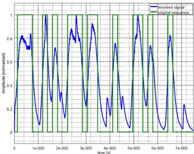
Fig. 10: Envelopes of a 32 bit pseudo-random binary sequence at a distance of 4 cm with power transmission running. Bit rate is 454.4 kbps. A properly selected detection threshold restores the bit sequence [1;1;1;0;0;1;0;1;0;0;1;1;1;0;1;1;0;0;0;1;0;0;0;1;1;0;1;0;0;0;1;0].
rates and the error performance demonstrate the potential of wideband gap devices for SWIPT applications.
REFERENCES
[1] S.Y.R. Hui, W. Zhong, and C.K. Lee, “A critical review of recent progress in mid-range wireless power transfer,”IEEE Transactions on Power Electronics, vol. 29, no. 9, pp. 4500–4511, Sept. 2014. [2] X. Wei, Z. Wang, and H. Dai, “A critical review of wireless power
transfer via strongly coupled magnetic resonances,” Energies, vol. 7, pp. 4316–4341, 2014.
[3] L. Liu, R. Zhang, and K.-C. Chua, “Wireless information and power transfer: A dynamic power splitting approach,”IEEE Transactions on Communications, vol. 61, no. 9, pp. 3990–4001, Sep. 2013.
[4] I. Krikidis, S. Timotheou, S. Nikolaou, G. Zheng, D. W. K. Ng, and R. Schober, “Simultaneous wireless information and power transfer in modern communication systems,”IEEE Communications Magazine, vol. 52, no. 11, pp. 104–110, Nov. 2014.
[5] S. Bi, Y. Zeng, and R. Zhang, “Wireless powered communication networks: An overview,”IEEE Wireless Communications, vol. 23, no. 2, pp. 10–18, Apr. 2016.
[6] T. Bieler, M. Perrottet, V. Nguyen, and Y. Perriard, “Contactless power and information transmission,”IEEE Transactions on Industry Applica-tions, vol. 38, no. 5, pp. 1266–1272, Sep./Oct. 2002.
[7] J. Wu, C. Zhao, Z. Lin, J. Du, Y. Hu, and X. He, “Wireless power and data transfer via a common inductive link using frequency division multiplexing,” IEEE Transactions on Industrial Electronics, vol. 62, no. 12, pp. 7810–7820, Dec. 2015.
[8] L. Shi, Z. Yin, L. Jiang, and Y. Li, “Advances in inductively coupled power transfer technology for rail transit,”CES Transactions on Elec-trical Machines and Systems, vol. 1, no. 4, pp. 383–396, Dec. 2017. [9] M. Liu, S. Liu, and C. Ma, “A high-efficiency/output power and
low-noise megahertz wireless power transfer system over a wide range of mutual inductance,” IEEE Transactions on Microwave Theory and Techniques, vol. 65, no. 11, pp. 4317–4325, Nov. 2017.
[10] O. Knecht and J. W. Kolar, “Comparative evaluation of IPT resonant circuit topologies for wireless power supplies of implantable mechanical circulatory support systems,” inProc. IEEE Applied Power Electronics Conference and Exposition (APEC), Tampa, FL, 2017, pp. 3271–3278. [11] A. P. Sample, D. A. Meyer, and J. R. Smith, “Analysis, experimental results, and range adaptation of magnetically coupled resonators for wireless power transfer,”IEEE Transactions on Industrial Electronics, vol. 58, no. 2, pp. 544–554, Feb. 2011.
[image:6.612.56.293.161.308.2] [image:6.612.71.280.433.558.2]