Coplanar Waveguide Band Reject Filter Using Electromagnetic Band
Gap Structure
Makarand G. Kulkarni1, *, Alice N. Cheeran1, Kamla P. Ray2, and Sandeepak S. Kakatkar3
Abstract—This paper presents design and analysis of six different configurations of Coplanar Waveguide Band Reject Filters (CPW-BRF) using Rectangular Dumbbell Electromagnetic Band Gap (RDEBG) cell structures. The performance in terms of rejection bandwidth, attenuation, cutoff characteristics of the proposed design are found superior to the earlier reported CPW-BRF. Using cascading of six RDEBG cells, rejection bandwidth has been improved up to 2.8 GHz with attenuation of −38.8 dB and filter selectivity of 26.9 dB/GHz. In addition, the radiation losses have also been analyzed by extracting equivalent R, L and C values from electromagnetic (EM) simulation results. Fabricated CPW-BRF using four RDEBG cells has been analyzed. For the fabricated CPW-BRF simulated and measured results are found in good agreement.
1. INTRODUCTION
Band Reject Filters (BRF) play an extremely important role in microwave and wireless applications provided by a wide variety of portable digital devices such as pocket and laptop computers, smart mobile phones, automobile navigators, and many wireless consumer devices. In this paper, BRF is designed using the Coplanar Waveguide (CPW) proposed by Wen in 1969 [1]. Compared with microstrip structures, the CPW structure is more attractive because it requires only a single metal level and offers greater design flexibility as well as ease of fabrication. The BRF can be implemented with shunt stubs or stepped-impedance lines in a microwave circuit [2]. The stepped-impedance filters are popular because they are easier to design and take comparatively less space than similar filters using stubs. However, because of the approximations involved, their electrical performance is often less than optimum. Also, the conventional design requires a larger circuit size which limits its applications, hence it is of limited use in portable RF/wireless communication systems. In 1987, Yablonovitch [3] and John [4] proposed Photonic Band Gap (PBG) cell structure (or the term Electromagnetic Band Gap (EBG) cell structures, usually preferred in the microwave community). EBG cell structures are periodic arrays of Defected Ground Structure (DGS), to prevent the propagation of electromagnetic waves in a certain frequency band. The DGS have a number of attractive features, such as simplicity in design, wider and deeper rejection band than that of a conventional filter, and easy circuit modeling [5–7], as elaborated in [5]. The EBG structures have two main properties: slow wave propagation in passband and band-stop characteristics [8]. Slow wave propagation phenomenon in passband is used for compacting microwave structures, whereas the stopband is useful for suppressing unwanted surface waves. Because of these two properties, these structures have found many applications in microwave circuits such as filters, power amplifiers, dividers, microwave oscillator and harmonic control in microstrip antennas [8].
Received 2 July 2017, Accepted 6 September 2017, Scheduled 12 September 2017
* Corresponding author: Makarand G. Kulkarni ([email protected]).
1 Department of Electrical Engineering, VJTI, Mumbai, Maharashtra State, India.2Department of Electronics Engineering, Defense
printed circuit board (PCB) area and hence had a limitation in microwave integrated circuit (MIC) applications. Also, a few more complex EBG structures have been proposed in [10]. A rectangular dumbbell-shaped DGS was explored for the first time by Ahn et al. and applied to design a low-pass filter on microstrip lines [5]. In [11], a CPW-BRF designed using seven square dumbbell-shaped DGSs in cascade has been shown to give wide rejection bandwidth of 2.8 GHz, but with low filter selectivity and high radiation losses. A CPW-BRF with periodic cascading of four spiral-shaped DGSs has been presented in [12]. However, it resulted in a comparatively narrow rejection bandwidth of 0.28 GHz. In the proposed work, designs of six different configurations of CPW-BRF using RDEBG have been carried out. The comparative performance analysis of all the six designs has been done in terms of cutoff frequency at−3 dB, resonant frequency, rejection bandwidth at−20 dB, filter selectivity, etc. Based on this analysis, the optimum design of CPW-BSF has been fabricated and tested. The performance of the proposed BRF has also been compared and discussed with the earlier reported CPW-BRF.
2. DESIGN
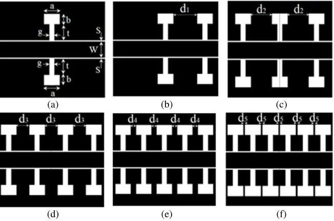
The CPW of characteristic impedanceZ0 = 50 Ω has been designed at 2.5 GHz, with a length of 40.2 mm,
strip width of W = 6 mm, and gap spacing ofS = 0.5 mm. The six design layouts of CPW-BRF with RDEBG are shown in Fig. 1. Fig. 1(a) shows a layout of CPW-BRF with single RDEBG with following dimensions a = 6 mm, b = 3.92 mm, g = 2 mm, t = 6 mm, and all these dimensions have been kept same for each RDEBG cell shown in Fig. 1(b) to Fig. 1(f), which depicts the layouts of CPW-BRF with cascading of two, three, four, five, and six RDEBG cells, respectively. In this work, the attempt is to get wide rejection bandwidth (RBW) with attenuation level (αmin which is the S21 value at transmission
zero) better than 20 dB near the desired resonance (3.17 GHz) using cascading configurations of EBG cells, keeping the dimensions of the EBG cells same, by optimizing the distance between EBG cells ‘d’. From Fig. 1(b) to Fig. 1(f), the distance between the two successive RDEBG cells is denoted by d1 = 9 mm, d2 = 8 mm, d3 = 4.75 mm, d4 = 2 mm, d5 = 0.55 mm respectively. The PCB size for all
the configurations is 40.2 mm×36 mm with the substrate material of dielectric constant εr = 4.5, loss tangent tan δ= 0.002, and substrate thickness of 1.6 mm.
(b)
(a) (c)
(e)
(d) (f)
Figure 2. Equivalent RLC model of an EBG cell [13].
Figure 2 shows the equivalent circuit model of an EBG cell, which consists of a parallel Resistor (R), Inductor (L), and Capacitor (C), elements connected in series with the transmission line, and these values can be calculated as given in Eqs. (1)–(3) [13, 14], where, fC and f0 imply cutoff frequency
and resonant frequency, respectively. The capacitance C is due to stored charges at the gap. The inductanceL comes from the additional magnetic flux flowing through the two apertures, andR is due to the radiation effect. The radiation losses are calculated using Eq. (4) [14]. It is clear from Eq. (4) that whenR goes to infinity (lossless), the radiation loss due to EBG structure becomes zero.
R = 2Z0
1 |S21|−
1
(1)
C = fC
4πZ0
f02−fC2 (2)
L = 1
4πf2 0C
(3)
η = 1
R 4Z0
+Z0 R + 1
(4)
3. RESULTS AND DISCUSSION
The IE3D [15] simulation results for scattering parameters of all the six configurations of proposed CPW-BRF are shown in Fig. 3 and Fig. 4. The extracted equivalentR,L,C values are listed in Table 1 for both the resonant frequencies. In Table 1, equivalent R1, L1,C1, and R2,L2,C2 values are given
respectively for the first transmission zero at resonant frequency f01 and for the second transmission
zero at resonant frequency f02. Table 2 gives the comparative performance analysis of six different
configurations of the proposed CPW-BRF. This analysis has been carried out with respect to cutoff frequency at −3 dB (fC), resonant frequency (f0), rejection bandwidth (RBW) at −20 dB rejection,
filter selectivity, attenuation at transmission zero, sharp rate of cutoff or sharpness factor (SF) given by Eq. (5) [16], radiation losses (% η) and quality factor [17] which is equal to 2πf0RC. Filter selectivity
is the rate of the roll-off of the transfer function of the filter between the passband frequency (fp) and stopband frequency (fs). The smaller the difference is between the passband and stopband frequencies, the better is the selectivity, and it can be defined as in Eq. (6) [17].
SF = fC f0
(5)
ξ = αmin−αmax
f s−fp (6)
where, ξ = filter selectivity in dB/GHz, αmax = the 3 dB attenuation point,αmin = attenuation at f0,
fS =f0, and fC = 3 dB cutoff frequency.
Widening of RBW has been observed with increase in the number of cascading RDEBG cells (fromCase 4 to Case 6) with almost sameαmin. The highest filter selectivity (ξ) has been observed in
-45 -40 -35 -30 -25 -20 -15 -10
0 1 2 3 4 5 6 7 8 9 10
S11
(d
B
)
Frequency (GHz)
One RDEBG Cell Two RDEBG Cells Three RDEBG Cells Four RDEBG Cells Five RDEBG Cells Six RDEBG Cells
Figure 3. Comparison of all the six CPW-BRF based on return loss.
-45 -40 -35 -30 -25 -20 -15 -10
0 1 2 3 4 5 6 7 8 9 10
Frequency (GHz)
One RDEBG Cell Two RDEBG Cells Three RDEBG Cells Four RDEBG Cells Five RDEBG Cells Six RDEBG Cells
S12
(d
B
)
Figure 4. Comparison of all the six CPW-BRF based on insertion loss.
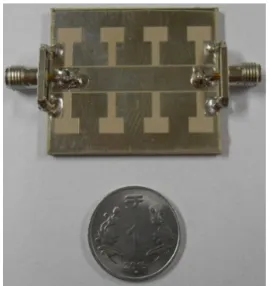
Figure 5. Fabricated proposed CPW-BRF.
-45 -40 -35 -30 -25 -20 -15 -10 -5 0
0 1 2 3 4 5 6 7 8 9 10
S-Parameters (dB) Frequency (GHz) S11_Simulation S11_Measured S21_Simulation S21_Measured
Figure 6. Comparison between simulated and measured results of fabricated CPW-BRF.
Table 1. Equivalent R,L,C, values for all six configurations.
Parameters CPW-BRF using RDEBG
Case 1 Case 2 Case 3 Case 4 Case 5 Case 6
No. of EBG cell 1 2 3 4 5 6
R1 (KΩ) 0.47 2.12 16.27 8.60 8.34 8.68
L1 (nH) 6.45 5.46 5.89 6.21 6.46 6.56
C1 (pF) 0.38 0.40 0.42 0.41 0.40 0.42
R2 (KΩ) 0.40 0.694 — 2.40 2.42 2.42
L2 (nH) 7.83 6.45 — 7.47 7.7 7.95
C2 (pF) 0.15 0.22 — 0.19 0.19 0.18
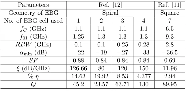
significantly fromCase 2 toCase6 compared to that inCase 1. Table 3 shows the comparative analysis of four different configurations of CPW-BRF with the spiral EBG geometry [12] and one design of that with the square EBG geometry [11]. It can be observed from Table 2 and Table 3 that CPW-BRF with the proposed four RDEBG cells (Case 4) provides wider RBW of 2.32 GHz, with higher αmin
Table 2. Comparative analysis of performances of all six configurations of CPW-BRF.
Parameters CPW-BRF with proposed RDEBG
Case 1 Case 2 Case 3 Case 4 Case 5 Case 6
No. of EBG cell used 1 2 3 4 5 6
fC (GHz) 1.73 1.94 1.82 1.75 1.71 1.67
f01 (GHz) 3.17 3.36 3.19 3.13 3.10 3.0
f02 (GHz) 4.5 4.2 — 4.15 4.12 4.11
RBW (GHz) — 0.77 0.58 2.32 2.44 2.8
αmin (dB) −15.2 -26.95 −44.28 −38.80 −38.53 −38.87
SF 0.545 0.577 0.570 0.559 0.551 0.556
ξ (dB/GHz) 8.47 16.80 30.02 25.96 25.56 26.99
% η 18.49 6.62 1.21 1.78 1.82 1.76
Q 3.71 18.38 137.3 70.30 66.18 70.09
Table 3. Performances of earlier reported works on CPW-BRF.
Parameters Ref. [12] Ref. [11]
Geometry of EBG Spiral Square
No. of EBG cell used 1 2 3 4 7
fC (GHz) 1.1 1.1 1.1 1.1 6.5
f01 (GHz) 1.25 1.3 1.3 1.3 9.3
RBW (GHz) 0.1 0.1 0.25 0.28 2.8
αmin (dB) −22 −19 −27 −33 −36.5
SF 0.88 0.84 0.84 0.84 0.69
ξ (dB/GHz) 126.66 80 120 150 11.96
%η 14.63 19.92 8.53 4.377 2.94
Q 45.2 23.57 63.71 130 89.95
been reported in [11] using seven EBG cells of square geometry. In the present work, the same RBW has been obtained using only six RDEBG cells. Also, better filter selectivity of 16.8 dB/GHz has been obtained using only two RDEBG cells compared to 11.96 dB/GHz using seven EBG cells of square geometry [11]. As seen from Table 2, by increasing number of RDEBG cells (from Case 3 to Case 6), higherαmin with lesser radiation losses has been obtained in the proposed work than that reported by
Lim et al. 2002 [12] as shown in Table 3, with moderate SF (0.559 for Case 4). Hence, it becomes apparent that CPW-BRF using only four RDEBG cells (Case 4) shows better performance than that reported in earlier work [11, 12]. Further, as shown in Fig. 5,Case 4 of CPW-BRF has been fabricated to achieve the best performance parameters and tested on Vector Network Analyzer. Fig. 6 shows the performance of the proposed BRF in terms of the scattering parameters. The measured and simulated results are in good agreement.
4. CONCLUSION
The rejection bandwidth of 2.8 GHz is achieved in the present work with only six RDEBG cells, which is equivalent to the reported work done using seven EBG cells of square geometry. In addition, an improvement in other performance parameters has also been observed. This CPW-BRF can be used as an alternative to the existing BRF in many microwave and wireless portable devices for wide stopband applications.
REFERENCES
1. Wen, C. P., “Coplanar waveguide: A surface strip transmission line suitable for nonreciprocal gyro-magnetic device applications,” IEEE Trans. on Microwave Theory and Techniques, Vol. 17 No. 12, 1087–1090, 1969.
2. Pozar, D. M., Microwave Engineering, 4th edition, John Wiley & Sons, New Delhi, 2012.
3. Yablonovitch, E., “Inhibited spontaneous emission in solid-state physics and electronics,” Physical Review Letters, Vol. 58, No. 20, 2059–2062, May 1987.
4. John, S., “Strong localization of photons in certain disordered dielectric superlattices,” Physical Review Letters, Vol. 58, No. 23, 2486–2489, June 1987.
5. Ahn, D., J. S. Park, C. S. Kim, J. Kim, Y. Qian, and T. Itoh, “A design of the low-pass filter using the novel microstrip defected ground structure,” IEEE Trans. Microwave Theory Tech., Vol. 49, 86–93, Jan. 2001.
6. Killamsetty, V. K. and B. Mukherjee, “Compact wideband bandpass filter for TETRA band applications,” IEEE Microwave and Wireless Components Letters, Vol. 27, No. 7, 630–632, Jul. 2017.
7. Kumar, A. and A. K. Verma, “Extraction of T and PI circuit models of microstrip line with defected ground structure,”International Conference on. Communications and Signal Processing (ICCSP), IEEE, 2011.
8. Dalili Oskouei, H., K. Forooraghi, and M. Hakkak, “Guided andleaky wave charactristics of periodic defectde ground structures,” Progress In Electromagnetics Research, Vol. 73, 15–27, 2007.
9. Martine, F., F. Falcone, J. Bonache, T. Lopetegi, M. A. G. Laso, and M. Sorolla, “Dual electromagnetic band-gap cpw structures for filter applications,” IEEE Microwave Wireless Components Lett., Vol. 13, 393–395, Sep. 2003.
10. Zoul, Y., X. Hu, S. He, and Z. Lin, “Compact coplanar waveguide lowpass filter using a novel electromagnetic bandgap structure,” Proceedings of 7th International Symposium on Antennas
Propagation & EM Theory, 1–4, 2006.
11. Yun, T. Y. and K. Chang, “Uniplanar one-dimensional photonic bandgap structures and resonators,”IEEE Trans. Microwave Theory Tech., Vol. 49, 549–553, Mar. 2001.
12. Lim, J.-S., C.-S. Kim, Y.-T. Lee, D. Ahn, and S. Nam, “A spiral-shaped defected ground structure for coplanar waveguide,”IEEE Microw. Wireless Compon. Lett., Vol. 12, No. 9, 330–332, Sep. 2002. 13. Lin, S.-Y., W.-Z. Tian, S.-Q. Zheng, and X.-W. Sun, “A semicircle DGS with high Q factor for microstrip line and low-pass filter,”Proceedings of Asia-Pacific Microwave Conference, 1197–1199, 2006.
14. Kim, H.-M. and B. Lee, “Bandgap and slow/fast-wave characteristics of defected ground structures including left-handed features,”IEEE Trans. Microw. Theory and Tech., Vol. 54, No. 7, 3113–3120, Jul. 2014.
15. Zeland Software Inc., IE3D Version 12.
16. Smierzchalski, M., P. Kurgan, and M. Kitlinski, “Improved selectivity compact band-stop filter with gosper fractal-shaped defected ground structures,”Microwave and Optical Technology Letters, Vol. 52, No. 1, 227–229, Jan. 2010.
![Figure 2. Equivalent RLC model of an EBG cell [13].](https://thumb-us.123doks.com/thumbv2/123dok_us/7738605.1267463/3.612.223.395.79.163/figure-equivalent-rlc-model-ebg-cell.webp)