ABSTRACT
CHO, YONGHWAN. Islanding and Seamless Reconnection of Multiple Solid-State Transformers Based On Droop Control. (Under the direction of Subhashish Bhattacharya.)
Solid state transformer (SST) is an emerging power electronics-based technology that
can replace traditional distribution transformers and actively manage renewable energy
resources, energy storage devices, and residential loads. The SST has been focused on due to
its low volume and weight which is achieved by using high-frequency AC-link transformer
instead of 50/60 Hz. Moreover, SST itself has features of reactive power compensation,
har-monic current filtering, and fault ride through capability while the conventional distribution
system needs additional equipments such as static synchronous compensator (STATCOM),
unified power flow controller (UPFC), unified power quality conditioner (UPQC), etc.
The SST is a core component of a smart distribution system, Future Renewable Electric
Energy Delivery and Management (FREEDM) system. By taking advantage of DC bus that
SST provides, DC microgrid can be easily integrated to the SST-based distribution system.
The renewable energy sources or energy storage devices of the DC microgrid can be used for
saving energy and more reliable operation of the distribution system, for example, islanding
operation. Wireless communication and power management system of the FREEDM also
improves the stability and controllability of the distribution system.
Among many functionalities of the FREEDM system, the autonomous islanding is
investigated in this thesis to attain fault ride-through capability when the system is islanded
from the utility. Moreover, a method is developed to achieve smooth reconnection to the grid
after a fault is cleared. The main component of the proposed control strategy is the control
of the high-voltage side converter of the SST, which is based on a combination of droop
(DAB), Distribued Energy Storage Device (DESD), and the Distributed Renewable Energy
Resources (DRER) are also developed and presented in detail. The harmonic compensation
scheme of the SST is also presented including a novel hybrid harmonic compensation
(HHC) method. The novel virtual impedance is also developed to cope with the wide range
of the grid impedance. A low-voltage scaled SST system is introduced, and the controllers
of the converters within the system are described. The proposed control strategy has been
tested in simulation and experimentally on a low-voltage scaled testbed.
The stability of the system that consists of the parallel connected voltage source inverters
is analyzed and a framework for the stability analysis is provided. The impedance based
models of the voltage source inverters are derived from large signal models. Solving the
impedance based circuit diagram of the overall power system, the current of the inverter
can be expressed by the sum of the transfer functions. The stability of the system can be
determined by analyzing the poles and zeros of the transfer functions. It is shown that the
grid impedance and the line impedance between SSTs can degrade the damping ratio of
the system and even make the system unstable if the controller bandwidth of the inverter
and the damping resistance are not selected propely with enough design margin. The
impedance based model and the criterion to determine the stability of the system are
© Copyright 2017 by Yonghwan Cho
Islanding and Seamless Reconnection of Multiple Solid-State Transformers Based On Droop Control
by Yonghwan Cho
A dissertation submitted to the Graduate Faculty of North Carolina State University
in partial fulfillment of the requirements for the Degree of
Doctor of Philosophy
Electrical Engineering
Raleigh, North Carolina
2017
APPROVED BY:
David Lubkeman Mesut Baran
Xiangwu Zhang Subhashish Bhattacharya
DEDICATION
To my parents Mr. Sung-Il Cho and Mrs. Aisa Kang, and my brother Mr. Soohwan Cho.
BIOGRAPHY
Yonghwan Cho was born in Seoul, the capital of South Korea. He received his Bachelor of
Science degree in Electrical Engineering from Seoul National University, Seoul, Korea, in
2012. In 2012, he joined the Department of Electrical and Computer Engineering at North
Carolina State University, Raleigh, North Carolina as a Ph.D. Scholar. His research interests
include Power Electronics, Solid-State Transformers, Grid-connected Converters, DC/DC Converters, Renewable Energy Integration, Motor Drives. He also worked as a Research
Assistant at the NSF FREEDM Systems Center and a Teaching Assistant of NCSU.
From 2008 to 2011, he was with MELFAS Inc, Seoul, South Korea, as a Research Engineer
in the Advanced Technology Department working on Automated Test Equipment that
verifies the functionality of capacitive touch sensor ICs. From May to August 2014, he
worked as an intern in Power Electronics Team of TESLA, Palo Alto, California, conducting
ACKNOWLEDGEMENTS
Thank my God that he sent me to this beautiful place. Though I sometimes had a hard
time pursuing a doctoral degree, I learned not only academical knowledge but also the
knowledge of God. I appreciate to all of the memebers of the youth group of Duraleigh
Presbyterian Church and Hanmaum Church. I realized later that I had much love and
comfort from the communities that I could stay strong.
I would like to express my sincere gratitude to my Ph.D. advisor, Dr. Subhashish
Bhat-tacharya, who gave me the opportunity of pursuing Ph.D. in Power Electronics and
sup-ported me during the past five years. I could grow as an independent researcher under
his guidance and support working on interesting and challenging projects related to the
Solid-State Transformer. I feel thankful for his consistant trust and encouragement.
I got many help from faculties and staffs in the FREEDM system center. I appreciate
especially my committee members, Dr. David Lubkeman and Dr. Mesut Baran for their
suggestions and feedbacks to deepen and improve my research and dissertation. Thanks
Dr. Xiangwu Zhang from the college of textiles for serving as the graduate representative in
my Ph.D. committee. I would like to thank Ms. Karen Autry for her kindness and love, Mr.
Hulgize Kassa and Dr. Leonard White for their help in lab and funny jokes.
I would like to extend my sincere thanks to Dr. Sungmin Kim, Dr. Yongsu Han, and Dr.
Byeongheon Kim for their guidance, ideas, and discussions. It was my great honor to meet
them. I learned a lot from them, not only Power Electronics but also their attitudes and
interests toward research. I also give thanks to Dr. Kuijun Lee for his advice and kindness.
Thanks to many nice and smart colleagues in the FREEDM system center. I would like to
thank Dr. Sachin Madhusoodhanan, Dr. Ankan De, and Richard Byron Beddingfield who I
their kindness and academic discussions with me.
My gratitude goes to Dr. Woongje Sung, Dr. Inhwan Ji, Dr. Seunghun Baek, Dr. Kibok
Lee, Kijeong Han, Jaehyuk Won and Heonyoung Kim. It was fun to talk and hang out with
them in and out of the FREEDM system center. Thank Jongbeom Park and Shinyoung Kwag
for the time we prayed and shared our lives .
Lastly, I would like to thank my parents and brother for their love and support. Though I
lived away from them during my Ph.D. studies, I know their pray, advice, and encouragement
TABLE OF CONTENTS
LIST OF TABLES . . . viii
LIST OF FIGURES. . . ix
Chapter 1 INTRODUCTION. . . 1
1.1 Research background . . . 1
1.2 Research purpose . . . 10
1.3 Thesis structure . . . 13
Chapter 2 REVIEW AND ANALYSIS OF EXISTING STRATEGIES . . . 14
2.1 Black start operation of SST-based system and autonomous islanding of microgrid . . . 15
2.1.1 Strategies for black start operation of SST-based system . . . 15
2.1.2 Strategies for autonomous islanding of microgrid . . . 16
2.2 Active synchronization methods and seamless reconnection of microgrid . 27 2.3 Current harmonic compensation of LCL-filtered voltage source converter (VSC) . . . 31
2.4 Controller design of the Dual Active Bridge (DAB) . . . 35
Chapter 3 PROPOSED CONTROL STRATEGIES FOR SST-BASED SYSTEM . . . 41
3.1 Control strategy of islanding SST . . . 51
3.1.1 LCL-filtered H-bridge : AC/DC of SST . . . 52
3.1.2 Dual Active Bridge (DAB) : DC/DC of SST . . . 69
3.1.3 Buck/Boost converter : DRER/DESD . . . 74
3.2 Control strategy of load SST . . . 80
3.2.1 LCL-filtered H-bridge : AC/DC of SST . . . 81
3.2.2 Dual Active Bridge (DAB) : DC/DC of SST . . . 92
3.2.3 Buck/Boost converter : DRER/DESD . . . 93
3.3 Islanding operation of SST-based system . . . 98
3.3.1 Islanding operation of the low-voltage scaled testbed . . . 98
3.3.2 Scalability of islanding operation of SST-based system . . . 106
3.3.3 Analysis of transition from grid-connected mode to islanded mode . 112 3.4 Seamless reconnection of SST-based system . . . 123
3.4.1 Seamless reconnection of the low-voltage scaled testbed . . . 123
3.4.2 Scalability of seamless reconnection of SST-based system . . . 129
Chapter 4 STABILITY ANALYSIS OF PARALLEL CONNECTED INVERTERS . . . 135
4.1.2 Impedance model of voltage controlled inverter connected to grid . 143
4.2 Stability analysis of testbed based on impedance model . . . 151
4.2.1 Stability analysis of testbed operating in grid-connected mode . . . . 151
4.2.2 Stability analysis of testbed operating in islanded mode . . . 159
Chapter 5 EXPERIMENTAL RESULTS. . . 165
5.1 Configuration of low-voltage scaled testbed . . . 165
5.2 Grid-connected operation of the low-voltage scaled testbed . . . 169
5.3 Islanding operation of the low-voltage scaled testbed . . . 174
5.4 Seamless reconnection of the low-voltage scaled testbed . . . 181
Chapter 6 CONCLUSION AND FUTURE WORK . . . 184
LIST OF TABLES
Table 1.1 Components of the Flexible AC Transmission System (FACTS). . . 5
Table 3.1 Testbed Parameters . . . 44
Table 3.2 Parameters of the proposed droop method. . . 60
Table 3.3 Parameters of the capacitor voltage controller . . . 64
Table 3.4 Simulation parameters of the harmonic compensation scheme of the islanding SST. . . 70
Table 3.5 Simulation parameters of the hybrid harmonic compensation (HHC) scheme of the load SST. . . 88
Table 3.6 Simulation parameters of the five-SST system used to verify the island-ing operation. . . 106
Table 4.1 Parameters of the current controlled inverter . . . 140
Table 4.2 Parameters of the voltage controlled inverter . . . 146
Table 4.3 Simulation parameters of the low-voltage scaled testbed . . . 155
Table 4.4 Simulation parameters of the low-voltage scaled testbed operating in islanded mode . . . 162
LIST OF FIGURES
Figure 1.1 Block diagram of the power system of the United States. . . 3
Figure 1.2 Block diagram of the Solid-State Transformer (SST). . . 3
Figure 1.3 The architecture of the Future Renewable Electric Energy Delivery and Management (FREEDM) system. . . 7
Figure 2.1 The active and reactive power flow through an inductor. . . 17
Figure 2.2 Droop characteristics of the synchronous generator. (a) Character-istic of speed and active power. (b) CharacterCharacter-istic of voltage and reactive pwoer. . . 18
Figure 2.3 Circuit diagram of voltage source inverter (VSI) for single-phase sys-tem. (a) LC-filtered VSI. (b) LCL-filtered VSI. . . 19
Figure 2.4 Conventional droop method. (a) frequency droop method. (b) mag-nitude droop method. . . 21
Figure 2.5 Block diagram of the conventional droop controller. . . 23
Figure 2.6 Block diagram of the multiloop controller of the LCL-filtered converter. 25 Figure 2.7 The virtual impedance implementation technique. . . 27
Figure 2.8 Block diagram of the microgrid and utility interfaced with static trans-fer switch (STS). . . 28
Figure 2.9 Block diagram of the synchronization controller. (a) Phase synchro-nization controller. (b) Voltage magnitude synchrosynchro-nization controller. 29 Figure 2.10 Block diagram of the current-controlled method (CCM) of the LCL-filtered converter with harmonic compensators. (a) Singleloop struc-ture. (b) Multiloop strucstruc-ture. . . 32
Figure 2.11 Circuit diagram of the dual active bridge (DAB). . . 35
Figure 2.12 Waveforms of the dual active brid (DAB) during one switching cycle. 36 Figure 2.13 Block diagram of the singleloop controller of the DAB. . . 39
Figure 2.14 Block diagram of the multiloop controller of the DAB. . . 39
Figure 3.1 Circuit diagram of the low-voltage scaled testbed. . . 42
Figure 3.2 Circuit diagram of the grid-connected SST and the DESD integrated into the low-voltage side DC link of the SST. . . 44
Figure 3.3 Three operation modes of the FREEDM system and the transitions of the operation modes. . . 45
Figure 3.4 Flow chart of the operation of the SST based system. (a) Flow chart of the FID. (b) Flow chart of the islanding SST. (c) Flow chart of the load SST. . . 47
Figure 3.5 The overall control strategy of the islanding SST. . . 48
Figure 3.6 The overall control strategy of the load SST. . . 50
Figure 3.8 The characteristic of the voltage magnitude droop curve. . . 54
Figure 3.9 Proposed droop method. (a) frequency droop method. (b) magnitude droop method. . . 56
Figure 3.10 Flow chart for generating the reference of the real power of the is-landing SST which is used for the autonomous isis-landing operation with the proposed droop method. . . 57
Figure 3.11 Block diagram of the proposed droop method. . . 59
Figure 3.12 Circuit diagram of the LCL filter of the AC/DC stage of the SST. . . 61
Figure 3.13 Block diagram of the singleloop capacitor voltage controller. . . 62
Figure 3.14 Bode diagram of the loop gain of the capacitor voltage controller. . . 64
Figure 3.15 Bode diagram analysis to verify the controller design. (a) Bode dia-gram of theTv c/(1+Tv c). (b) Bode diagram of theGg/(1+Tv c). . . 65
Figure 3.16 Step response of the active and reactive power of the proposed droop method and the capacitor voltage controller. . . 67
Figure 3.17 Block diagram of the current harmonic compensators of the islanding SST. . . 68
Figure 3.18 Simulation results without the harmonic compensation scheme. (a) Grid current waveform. (b) FFT of the grid current. . . 68
Figure 3.19 Simulation results with the harmonic compensation scheme. (a) Grid current waveform. (b) FFT of the grid current. . . 69
Figure 3.20 Circuit diagram of the dual active bridge (DAB). . . 70
Figure 3.21 Block diagram of the proposed controller of the DAB. . . 70
Figure 3.22 Step responses of the proposed DAB controller with three different controller bandwidths. . . 74
Figure 3.23 Circuit diagram of the bidirectional buck/boost converter of the is-landing SST. . . 75
Figure 3.24 Outer DC link controller of the buck/boost converter of the islanding SST. . . 75
Figure 3.25 Inner battery current controller of the bidirectional buck/boost con-verter of the islanding SST. . . 76
Figure 3.26 Step responses of the buck/boost controller with three different band-widths of the DC link controller. . . 78
Figure 3.27 Block diagram of the battery power controller of the islanding SST. . 78
Figure 3.28 Charging and discharging of the battery using the battery power controller. . . 79
Figure 3.29 Block diagram of the proposed multiloop controller of the LCL-filtered converter with a hybrid harmonic compensation scheme and a novel virtual impedance method. . . 82
Figure 3.32 Bode diagrams of the loop gains of the harmonic compensation sys-tems. (a) Loop gain of the harmonic current compensation (HCC) system. (b) Loop gain of the harmonic voltage compensation (HVC)
system. . . 86
Figure 3.33 Waveform of the grid current with the harmonic compensation of the 23rd harmonic current. (a) Grid current with the HCC of the outerloop. (b) Grid current with the HVC of the innerloop. . . 87
Figure 3.34 Simulation results with the hybrid harmonic compensation (HHC) scheme. (a) Grid current waveform. (b) FFT of the grid current. . . 88
Figure 3.35 Block diagram of the proposed virtual impedance method. . . 90
Figure 3.36 The step responses of the DC-link voltage and the grid current. (a) Without the grid impedance. (b) With the grid impedance. (c) With the grid impedance and only the feed forward of the virtual impedance method. (d) With the grid impedance and the whole virtual impedance method. . . 91
Figure 3.37 Step responses of the proposed DAB controller with three different controller bandwidths. . . 93
Figure 3.38 Step response of the battery current controller of the DESD of the load SST. . . 94
Figure 3.39 Circuit diagram of the DRER of the load SST. . . 95
Figure 3.40 Outer PV voltage controller of the DRER of the load SST. . . 95
Figure 3.41 Inner PV current controller of the DRER of the load SST. . . 96
Figure 3.42 Step response of the PV voltage controller of the DRER of the load SST. 97 Figure 3.43 I-V and P-V characteristics of the PV array used in the simulation. . . 98
Figure 3.44 Bidirectional power flow of the load SST with DRER. . . 99
Figure 3.45 Transient responses of the islanding of the low-voltage scaled testbed. (a) Transient response of the PCC current. (b) Transient response of the active and reactive power. (c) Transient response of the DC link voltages. (d) Transient response of the battery current. . . 101
Figure 3.46 Simulation results of the autonomous islanding with communication delay. (a) With communicaion delay of 100 msec. (b) With communi-cation delay of 200 msec. . . 103
Figure 3.47 Simulation results of the islanding operation when the power of the load SST varies due to the DRER. . . 105
Figure 3.48 Circuit diagram of the five AC/DC stages of the SST connected parallel to the utility grid through FID. . . 107
Figure 3.50 Simulation result of the islanding of the five-SST system when the sum of the power references of the islanding SSTs are larger than required. . . 110 Figure 3.51 Simulation result of the islanding of the five-SST system when the
sum of the power references of the islanding SSTs are smaller than required. . . 111 Figure 3.52 Circuit diagram of the five AC/DC stages of the SST connected parallel
to the utility grid through FID when line impedance exist between the islanding SSTs. . . 113 Figure 3.53 Simulation waveforms during the transition from the grid connected
mode to the islanding mode when line impedance exist between the islanding SSTs. . . 114 Figure 3.54 Simulation waveforms during the transition from the grid connected
mode to the islanding mode when islanding SSTs were drawing dif-ferent amount of actual power. . . 116 Figure 3.55 Simulation waveforms during the transition from the grid connected
mode to the islanding mode with three different inductance of the grid side inductor of the LCL filter. . . 118 Figure 3.56 Circuit diagram of the four AC/DC stages of the SST connected
paral-lel to the utility grid when line impedance exist between the islanding SSTs. . . 120 Figure 3.57 Circuit diagram of the four AC/DC stages of the SST operating in
islanded mode when line impedance exist between the islanding SSTs.122 Figure 3.58 Output power of the islanding SST1 and the islanding SST2 according
to different inductance of the grid side inductor of the LCL filter. (a)
LL1=LL2=1m H. (b)LL1=1m H andLL2=3m H. . . 123
Figure 3.59 Block diagram of the seamless reconnection method of the islanding SST located nearest to the PCC. . . 124 Figure 3.60 Block diagram of the seamless reconnection method of the islanding
SST connected in parallel with the SST located nearest to the PCC. . 125 Figure 3.61 Transient responses of the seamless reconnection of the low-voltage
scaled testbed. (a) Transient response of the PCC current. (b) Tran-sient response of the active and reactive power. (c) TranTran-sient response of the DC link voltages. (d) Transient response of the battery current. 128 Figure 3.62 Zoomed-in simulation results of the seamless reconnection. . . 130 Figure 3.63 Circuit diagram of the five AC/DC stages of the SST connected parallel
to the utility grid through FID. . . 131 Figure 3.64 Simulation result of the seamless reconnection of the five-SST system.132 Figure 3.65 Simulation waveform of the grid side current of the islanding SSTs
Figure 4.1 Circuit diagram of the AC/DC stage of the SST connected to the utility grid. . . 137 Figure 4.2 The block diagram of the singleloop current controller of the
LCL-filtered voltage source inverter in single-phase system. . . 137 Figure 4.3 The impedance based model of the current controlled AC/DC stage
of the SST. . . 139 Figure 4.4 The steady-state and transient response of the current controller of
the AC/DC stage of SST. (a) The grid current waveform when the controller bandwidth is 700 Hz. (b) The grid current waveform when the controller bandwidth is 1300 Hz. . . 141 Figure 4.5 The migration of poles and zeros of the internal resonance transfer
functionRc c when the controller bandwidth is changed from 500 Hz
to 1300 Hz. (500 Hz, 700 Hz, 900 Hz, 1100 Hz, 1300 Hz) . . . 142 Figure 4.6 The migration of poles and zeros of the internal resonance transfer
functionRc c when the grid impedance is increased from 0.1 mH to 5
mH. (0.1 mH, 1 mH, 3 mH, 5 mH) . . . 142 Figure 4.7 The migration of poles and zeros of the internal resonance transfer
functionRc c when the damping resistance is decreased to 1Ω. The
grid impedance is increased from 0.1 mH to 5 mH. (0.1 mH, 0.5 mH, 1 mH, 5 mH) . . . 143 Figure 4.8 Circuit diagram of the AC/DC stage of the SST connected to the utility
grid. . . 144 Figure 4.9 The block diagram of the singleloop voltage controller of the
LCL-filtered voltage source inverter in single-phase system. . . 144 Figure 4.10 The impedance based model of the voltage controlled AC/DC stage
of the SST. . . 145 Figure 4.11 The migration of poles and zeros of the internal resonance transfer
functionRv c when the controller bandwidth is changed from 500 Hz
to 1300 Hz. (500 Hz, 700 Hz, 900 Hz, 1100 Hz, 1300 Hz) . . . 147 Figure 4.12 The migration of poles and zeros of the internal resonance transfer
functionRv c when the grid impedance is increased from 0.1 mH to
10 mH. (0.1 mH, 1 mH, 5 mH, 10 mH) . . . 148 Figure 4.13 The migration of poles and zeros of the internal resonance transfer
functionRv c when the damping resistance is decreased to 2Ω. The
grid impedance is increased from 0.1 mH to 10 mH. (0.1 mH, 1 mH, 5 mH, 10 mH) . . . 148 Figure 4.14 The steady-state waveform of the grid current of the voltage
Figure 4.15 Admittance model of the low-voltage scaled testbed connected to
the utility grid. . . 150
Figure 4.16 Poles and zeros of the resonance functions of the grid-side current of the current controlled inverter. (a) Poles and zeros of the internal resonance function,R3. (b) Poles and zeros of the parallel resonance function,P3,1. (c) Poles and zeros of the series resonance function,S3. 154 Figure 4.17 Pole-zero map of the internal resonance function of the testbed when Lg r i d =Ll1=Ll2=0.1m H andLg r i d =Ll1=Ll2=2.0m H. (a) Pole-zero map of the internal resonance function,R3. (b) Zoomed in pole-zero map of the internal resonance function,R3. . . 156
Figure 4.18 Simulation waveform of grid side current of the current controlled inverter. (a) Grid side current whenLg r i d =Ll1=Ll2=0.1m H. (b) Grid side current whenLg r i d=Ll1=Ll2=2.0m H. . . 156
Figure 4.19 Pole-zero map of the internal resonance function of the testbed with different grid impedance and cable impedance. (a) Pole-zero map of the internal resonance function whenLg r i d =Ll1=Ll2=0.1m H. (b) Pole-zero map of the internal resonance function whenLg r i d = 5.0m H andLl1 = Ll2 =0.1m H. (c) Pole-zero map of the internal resonance function whenLl1=5.0m H andLg r i d =Ll2=0.1m H. (d) Pole-zero map of the internal resonance function whenLl2=5.0m H andLg r i d =Ll1=0.1m H. . . 158
Figure 4.20 Admittance model of the low-voltage scaled testbed operating in islanded mode. . . 160
Figure 4.21 Pole-zero map of the internal resonance function of the testbed oper-ating in islanded mode with different cable impedance. (a) Pole-zero map of the internal resonance function whenLl1=Ll2=0.1m H. (b) Pole-zero map of the internal resonance function whenLl1=5.0m H andLl2=0.1m H. (c) Pole-zero map of the internal resonance func-tion whenLl2=5.0m H andLl1=0.1m H. (d) Pole-zero map of the internal resonance function whenLL1=Ll2=5.0m H. . . 163
Figure 5.1 The low-voltage scaled testbed built in the lab. . . 166
Figure 5.2 The hardware structure of the islanding SST. . . 167
Figure 5.3 The battery pack and the power stage of the islanding SST. . . 167
Figure 5.4 The ZigBee module and the DSP board of the SST. . . 167
Figure 5.5 Instability phenomenon of the 13th harmonic compensator of the conventional single-loop current controller. . . 169
Figure 5.7 The step responses of the DC-link voltage and the grid current. (a) Without the grid impedance. (b) With the grid impedance. (c) With the grid impedance and only the feed forward of the virtual impedance method. (d) With the grid impedance and the whole virtual impedance method. . . 171 Figure 5.8 Step response of the active and reactive power of the AC/DC stage of
the islanding SST. . . 172 Figure 5.9 Step response of the proposed DAB controller and the conventional
small-signal based controller. . . 173 Figure 5.10 (a) Step response of the battery power controller. (b) Waveforms of
low-voltage side DC bus and the battery voltage. . . 174 Figure 5.11 The transient responses during the transition period of the operation
from grid-connected mode to islanding mode. (a) PCC current (FID current). (b) Grid powers. (c) MV DC link voltages. (d) LV DC link voltages. (e) DESD battery voltages. (f ) DESD battery currents. . . 176 Figure 5.12 Transient responses of the active power of the SSTs during the
transi-tion from grid-connected mode to islanded mode when the commu-nication delay exists. . . 178 Figure 5.13 Transient responses of the SSTs during the transition from grid-connected
mode to islanded mode when line impedance between islanding SSTs is 5mH. (a) Transient responses of the active power of the SSTs . (b) Transient responses of the medium-voltage side DC bus. . . 179 Figure 5.14 Transient responses of the SSTs during the transition from grid-connected
mode to islanded mode when line impedance between islanding SSTs is 5mH and the droop slope is increased for 150 msec. (a) Transient responses of the active power of the SSTs . (b) Transient responses of the medium-voltage side DC bus. . . 180 Figure 5.15 The transient responses during the transition period of the operation
from islanding mode to grid-connected mode. (a) PCC current (FID current). (b) Grid powers. . . 182 Figure 5.16 The transient responses during the transition period of the operation
CHAPTER
1
INTRODUCTION
1.1
Research background
The semiconductor power devices have been developed widely after the initial replacement
of vacuum tubes by solid-state devices in the 1950s[1]. The first development was bipolar power device, such as bipolar transistors and thyristors made from silicon. Due to
advan-tages of using the power devices over vacuum tube, many efforts have been made aiming to
switching speed and replaced bipolar transistors at applications for high switching speed.
To overcome the issues of bipolar devices and power MOSFETs, insulated gate bipolar
tran-sistor (IGBT) was developed in 1980s which has huge advantage in increasing voltage and
current ratings of the device. Today the power devices are being more and more efficient by
using wide bandgap materials, such as silicon carbide (SiC) and gallium nitride (GaN).
Along with the advancement of the power device technology, research on power
elec-tronics has been focused on to improve many aspects of power conversion using the power
devices. Due to the fast switching capability and low on-resistance of the power devices,
the volume of the power converter is reduced and the efficiency is increased. Moreover,
power electronics provide controllability of voltage and current and thus, can be used
for wide range of applications meeting the system requirement. For example, the speed
of the electric motors can be controlled accurately and the state of charge (SOC) of the
battery of the electric vehicle can be managed by controlling the current and voltage of the
battery charger. Also high-voltage direct current (HVDC) is developed for transmitting large
amounts of electricity over long distances which converts several hundreds of kilovolts of
AC to DC.
Solid-state transformer (SST) is an emerging technology which is for replacing
tradi-tional distribution level power transformer with converters made up of the solid-state
devices[2],[3]. Fig. 1.1 shows the block diagram of the power system of the United States [4]. The transmission level of several hundreds of kilovolts are stepped down to distribution level of several tens of kilovolts. It is again stepped down to residential level of 120/240 V by distribution level power transformer. The SST is not only able to interface the distribution
Generating station Generator Transmission substation Distribution substation Customer 120/240V Transmission line customer Subtransmission customer Generator step-up transformer Step-down power transformer Step-down power transformer Distribution transformer (1~20 customers) Main transmission
138kV, 230kV, 345kV, 500kV, 765kV
Sub-transmission 115/121kV, 60/69kV
Distribution 11/12kV, 13.8kV, 35kV
Figure 1.1Block diagram of the power system of the United States.
AC DC DC AC AC DC DC AC Medium-frequency
isolated DC/DC stage
Figure 1.2Block diagram of the Solid-State Transformer (SST).
has many advantages coming from power electronics technology.
The SST typically consists of 3 stages of power converters, AC/DC, DC/DC and DC/AC, as shown in Fig. 1.2. While the conventional transformer operates with 50/60 Hz, the SST uses medium-frequency (10-20 kHz) in its DC/DC stage. Since the volume of the transformer is inversely proportional to the cube of the frequency, the volume and weight of the SST
the efficiency of this stage can be increased to 99%. If the SiC devices are used, the overall
efficiency of the SST can be competitive with that of the traditional distribution level power
transformer.
Besides the advantage of the volume and weight, the SST can provide controllability
to the distribution power system, such as power factor correction and current harmonics
compensation. While the traditional passive transformer does not have any functionality
other than the voltage step down and the galvanic isolation, the SST itself has many power
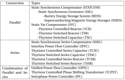
electronics based features. For example, Flexible AC Transmission System (FACTS) requires
different types of equipments as shown in Table 1.1. The FACTS is a power electronics based
system which is meant to increase power transfer capability by controlling the reactive
power of the power transmission system[9]. Since the traditional power transformers are passive components, the active components are needed : Static Synchronous Compensator
(STATCOM), Static Var Compensator (SVC), Unified Power Flow Controller (UPFC), etc.
However, if the SSTs are used instead of the conventional transformer, those equipments
are not needed and the SSTs themselves provide the controllability of the reactive power.
Due to the 3-stage structure, the SST provides DC bus of both the medium-voltage (MV)
and low-voltage (LV). It is another advantage of using SSTs in the distribution level power
system. Since the renewable energy sources (RESs) and energy storage systems (ESSs), such
as photovoltaics (PV) and battery, produce DC, it is more simple and easy to connect those
devices to the DC grid than the AC grid.
When electricity began to be used, there was a debate on selecting the transmission type
between AC and DC. It resulted in using AC system since stepping up the high-voltage to
Table 1.1Components of the Flexible AC Transmission System (FACTS).
Connection Types
Parallel
Static Synchronous Compensator (STATCOM) -Static Synchronous Generator (SSG)
-Battery Energy Storage System (BESS)
-Superconducting Magnetic Energy Storages (SMES) Static Var Compensator (SVC)
-Thyristor Controlled Reactor (TCR) -Thyristor Switched Reactor (TSR) -Thyristor Switched Capacitor (TSC)
Series
Static Synchronous Series Compensator (SSSC) Interline Power Flow Controller (IPFC)
Thyristor Controlled Series Capacitor (TCSC) Thyristor Switched Series Capacitor (TSSC) Thyristor Controlled Series Reactor (TCSR) Thyristor Switched Series Reactor (TSSR) Combination of
Parallel and Se-ries
Unified Power Flow Controller (UPFC)
Thyristor Controlled Phase Shifting Transformer (TCPST) Interphase Power Controller (IPC)
transformer windings. The invention of the induction motor expanded the AC system even
to the distribution level and the residential level.
DC power system has been expanded recently especially in the transmission level
high-voltage power system. The improvement of the ratings of the power devices and modular
multi-level converter (MMC) enabled the conversion of the high-voltage AC to DC. DC
system is also more efficient than AC system in transmitting large amount of electricity over
long distances. Thus, HVDC electric power transmission system is now being widely used.
However, DC grid of distribution level and residential level is not formed widely.
installed widely because most of the residential devices are based on AC and it takes a lot of
cost and effort to replace the whole AC system with DC system. Considering those aspects,
the SST can be a solution which both maximizes the usage of the current AC power system
and provides DC grid. The RESs and ESSs of either distribution level or residential level can
be connected to the DC links of the SSTs.
With the many merits of the SST, a SST-based microgrid system is proposed in 2008,
which is called Future Renewable Electric Energy Delivery and Management (FREEDM)
system. Fig. 1.3 shows the architecture of the FREEDM system. The MV grid is connected
to the SST through the fault isolation device (FID). The FID is a solid-state based circuit
breaker which is more efficient and has faster response than the conventional mechanical
circuit breaker[10],[11]. It isolates the SST from the MV grid when any fault is occured. The response time of the FID is nearly 100µs while that of the conventional one is 1-2
ms. The Distribued Renewable Energy Resources (DRERs) are the devices which interface
the RESs with the DC grid that the SST forms. Similarly, the Distributed Energy Storage
Devices (DESDs) connect the ESSs to the DC grid. DRER and DESD consist of DC/DC power converters. The distributed grid intelligence (DGI) is a software embedded in ARM
processor. Each component of the FREEDM system, FID, SST, DESD, and DRER, has both
ARM processor based board and DSP board. DSP board is for controlling the power stage and
the ARM board handles higher level control and communication among each component
of the FREEDM system to improve reliability and controllability of the system. Lastly, the
residential area AC loads, distributed AC generators, and solar micro-inverters can be
connected to the residential level AC grid of the SSTs.
Figure 1.3The architecture of the Future Renewable Electric Energy Delivery and Management (FREEDM) system.
into the current AC power grid system in the form of distributed generation (DG)[12]. These RESs-based DG system is typically installed with ESSs and forms AC microgrid at MV
distribution level or LV residential level. When the microgrid is operating in grid-connected
mode, RESs lessen the burden of the power grid by feeding a large portion of the system
loads and can even feed the power grid when the amount of power RESs produce exceeds
the system load. Moreover, another feature of the microgrid is autonomous islanding mode
in which the microgrid is operated solely by the RESs and ESSs without any interruption
when it is islanded from the power grid intentionally or unintentionally. Each DG unit
of the microgrid and benefits both the utility and customers.
The SST also has autonomous islanding mode for residential-level grid. The DRERs
and DESDs which are integrated into the LV side DC link (LVDC) of the SST can supply
power required in both the DC grid and the residential-level AC grid (LVAC) when the MV
AC grid is disconnected from the SST. In this operation mode, the AC/DC stage of the SST connected to the MV side and the medium-frequency isolated DC/DC stage are turned off, and only DRERs, DESDs, and AC/DC stage of the LV side operate.
However, if the SST does not have enough DRERs or DESDs, the residential are fed by the
SST will experience an outage. In this case, the typical solution is to restore the MV grid or
the LV grid with generating units, which is called black start. Black start is “a bottom-up type
of restoration that uses preselected generating units in the case of a widespread blackout,
whereas a top-down type of restoration is assisted by neighboring power grids only when a
portion of the power system experiences outages"[13]. The United States Department of Energy, in[14], has defined the black start capability as “the ability to go from a shutdown condition to an operating condition delivering electric power without assistance from the
electric system".
The black start operation of the SSTs has been introduced and the control methods
for a grid-connected operation and black start operation have been proposed in the
litera-ture[15]. In[16], SSTs are differentiated as master or slave and are controlled by proposed sequences by taking advantage of the communication capability of the FREEDM system.
Those methods restore the MV AC grid using the DRERs and DESDs. However, these
meth-ods change the controllers of the SSTs according to their operation modes, which results
pe-riod. Thus, more reliable and practical strategies are required to achieve uninterruptible
SST-based microgrid system.
The islanded microgrid needs to be reconnected seamlessly maintaining the power flow
of the microgrid when the power grid is restored and ready to be used[17]–[20]. The voltage at each end of the static transfer switch (STS) or the FID should be actively synchronized to
prevent overcurrent or overvoltage due to the voltage difference. A wireless communication
based method is proposed in[17]and a synchronization controller is presented in[18] for multiple DG units connected in parallel. Seamless reconnection strategy for FREEDM
system is needed where multiple SSTs operate in parallel.
With the increasing penetration of power electronics based power conversion such
as UPSs, DG systems, etc., regulating harmonic current has been an important issue and
admissible harmonic currents are limited according to standards, e.g. IEEE Std 519-1992.
The LCL-filtered voltage-source converter (VSC) has drawn much attentiondue to its better
attenuation of switching frequency current harmonics compared to L-filtered VSC[21]–[23]. However, the low-order harmonic current should be removed by harmonic
compen-sators (HCs) in order to prevent the grid from being polluted[24]–[26]. The HC is a resonant controller which is widely used in grid-connected converters and especially in
single-phase system[27]. The resonant controller is used in stationary reference frame while the synchronous PI controller is designed in synchronous reference frame. It is proved that
pro-portional+resonant (PR) regulator in the stationary reference frame and the synchronous PI regulator have same transient and steady-state performance[28]. The harmonic current can be regulated by adding the HCs for harmonic frequencies of interest in parallel with the
compen-sation is to add enough number of HCs to meet the THD standards and guarantee stability
of the converter at the same time. The maximum frequency of the HC is limited since the
phase margin of the harmonic compensation loop decreases as its harmonic frequency
increases. Moreover, the stability is worse if the grid impedance is large due to long cable or
transformer[24],[29].
In most cases, the SST is also connected to the MV power grid through the LCL filter.
Thus, it is important to design not only the controller of the LCL-filtered AC/DC stage at the grid fundamental frequency but also the HCs for regulating grid harmonic currents.
1.2
Research purpose
As mentioned in the previous section, the SST is an emerging technology that can replace
the traditional distribution-level power transfomer. The volume and weight of the SST can
be reduced due to the medium-frequency isolated DC/DC stage. With the advent of wide bandgap power devices and nanocrystalline core material, the efficiency of the SST is as
high as the conventional power transformer. By taking advantage of using power electronics
based converters, reactive power can be controlled without any other auxiliary equipments
used in FACTS, such as SVC, STATCOM, and UPFC.
The FREEDM system maximizes the advantage of using SST. The FID, DRER, DESD, and
DGI are other components of the FREEDM system and provide controllability and reliability
of the system. For example, the DRERs can produce power and feed the residential loads
reducing the power usage of the power grid. The DESDs can be used for peak shaving to
“reduce the amount of energy purchased from the utility company during peak hours when
Among the many functionalities of the FREEDM system, the autonomous islanding
operation of the FREEDM system of multiple SSTs is studied in this thesis. There are two
types of the autonomous islanding operation of the FREEDM system. One is the islanding
of the DC grid integrated into the DC link of the SST[31]. When the MV power grid is disconnected intentionally or unintentionally and the DC microgrid cannot be enabled by
the SST, the DRERs and DESDs autonomously form the DC grid with their energies and also
feed the residential AC system. The autonomous islanding of the DC grid is based on v-i
droop control which is implemented to the DESDs. The DRERs do not directly regulate the
DC grid but support the grid by producing renewable energy. The other type is the islanding
operation of the MV grid. If a SST has not enough power rating of DRERs and DESDs, it
needs to be fed by other sources connected to the point of common coupling (PCC) of the
MV power grid. The sources can be auxiliary generators or other SSTs tied to the PCC of
the MV. As mentioned before, the black start operation of the SSTs are presented in the
literatures[15],[16]. After the shutdown of the MV power grid, the restoring process of the MV line initiates using the SSTs which have large capability of the DRERs and DESDs. The
controller of the SSTs and DESDs changes according to the operation mode, grid-connected
or black start, or complicated communication is needed which result in unavoidable delays
of the power system restoration during the mode transition period. In this thesis, a new
control strategy is developed to maintain the MV at PCC without any blank time when the
FREEDM system is islanded so that SSTs without enough DRERs and DESDs can even be
operated in the autonomous islanding mode and the residential load can be fed without
facing the outage. The SSTs with abundant energy sources behave like UPSs to support
proposed and controllers for each stage of the SST and DESD are presented in detail.
In order for the islanded FREEDM system to be reconnected to the power grid after it is
recovered, a seamless reconnection scheme is needed. The voltages at both ends of the FID
should be actively synchronized firstly while maintaining the islanding operation and then
be reconnected without overcurrent or overvoltage issues. A novel seamless reconnection
scheme is studied to provide more reliable and practical method.
Regarding the harmonic current compensation, a major challenge is to add enough
number of HCs to meet the THD standards and guarantee stability of the converter at the
same time. To overcome the instability issue, phase compensation methods are presented
in[24],[32]. In those methods, conventional resonant HC is modified to have trigonometric terms to compensate the phase of it. In this thesis, a multi-loop controller is presented as a
possible replacement for the conventional grid current controller to have enough phase
margin at high harmonic frequencies without using trigonometric terms and to achieve
sufficient harmonics attenuation by implementing both harmonic current compensation
(HCC) and harmonic voltage compensation (HVC), namely a hybrid harmonic
compensa-tion (HHC). Convencompensa-tional multi-loop controller has an inner-loop of filter capacitor current
or converter-side inductor current to improve dynamic performance and achieve active
damping[22],[23],[25]. However, the proposed multi-loop controller has an inner-loop of filter capacitor voltage to provide not only the HHC but also a straightforward criteria of
setting the controller gain of the outer-loop. It should be noted that active damping is also
feasible with the proposed multiloop frame by using a feed forward method presented in
1.3
Thesis structure
This thesis has the following structure.
Chapter 1 is the introduction. It describes the background of the research, the purpose
of the research, and the structure of the thesis.
In chapter 2, the literature review of the islanding, seamless reconnection, and
har-monic compensation is presented and their limitations are discussed. The strategies for the
black start operation of the SSTs are shown firstly. Then the conventional droop method is
presented which is widely used in the DG systems and UPSs for the autonomous islanding
operation. Several schemes for the active synchronization and seamless reconnection are
depicted. Lastly, the harmonic current compensation schemes are reviewed.
Chapter 3 proposes novel strategies for the islanding, seamless reconnection, and
har-monic compensation. The structure of the controller of SST and DESD is described and the
design of the controller is also presented. New methods for both the seamless transition
from grid-connected mode to islanded mode, and from islanded mode to grid-connected
mode are suggested. A novel harmonic compensation scheme is described and compared
with the conventional strategy. All the strategies are verified through simulation results.
Chapter 4 shows experimental results to verify the proposed strategies. A low-voltage
scaled testbed is built to represent the FREEDM system with multiple SSTs. The testbed
with multiple SSTs is operated using wireless communication. The strategies are digitally
implemented in DSP controllers and the proposed schemes are verified experimentally.
CHAPTER
2
REVIEW AND ANALYSIS OF EXISTING
2.1
Black start operation of SST-based system and
autonomous islanding of microgrid
2.1.1
Strategies for black start operation of SST-based system
In the FREEDM system with multiple SSTs operating in parallel, the PCC voltage can be
restored by the black start operation using the DESDs and DRERs[15],[16]. In order to restore the PCC voltage, the controller of each stage of the SST and DESD is switched according to
the operation modes in[15]. During the grid-connected mode, the MV side AC/DC stage regulates the MV DC link by controlling the current of the MV grid. The dual active bridge
(DAB) controls the LV DC link. Provided the LV DC link, the DRER controls the voltage
of the PV panel according to the maximum power point tracking (MPPT) algorithm. The
DESD makes the current of the battery follow the reference value determined by a battery
management system (BMS). Once the system is islanded and the black start operation
initiates, the DESD controls the LV DC link, not the battery current. Provided the LV DC
link, the DAB regulates MV DC link. Finally, the MV side AC/DC stage controls the capacitor voltage of the LCL filter to restore the PCC voltage. To adjust power sharing of the SSTs
connected in parallel, the conventional voltage-frequency (V-f ) droop method is used to
calculate the reference of each capacitor voltage. The controller of the MV side AC/DC, DAB, and DESD, changes to achieve the black start operation and the delay between the
instance of the grid disconnection and black start restoration is unavoidable.
using the droop method. The slave SST works in the same way as the SST in grid-connected
mode which is described in[15]. The master and slave SSTs are controlled by proposed sequences by taking advantage of the communication capability of the FREEDM system.
However, the droop method is not used and no sequence for the parallel operation of the
master SSTs is presented.
2.1.2
Strategies for autonomous islanding of microgrid
The autonomous islanding is the key feature of the microgrid. It enables the uninterruptible
operation of the microgrid and increase reliability of the microgrid system. It benefits both
the utility and customers. For the islanding operation, the PCC voltage can be directly
controlled as proposed in[33]. In the paper, the MV side grid current is controlled during the grid-connected mode. When the islanding is detected, the PCC voltage controller is
enabled as an outer loop of the grid current controller. The output of the PCC voltage
controller determines the reference of the grid current which is necessary to regulate the
PCC voltage. However, this method occurs high current at the instance of the islanding
due to the sudden initiation of the outer loop. Moreover, it does not provide strategy for
operating multiple converters connected in parallel.
Changing the controller of the converter according to the operation mode is not
suit-able to achieve seamless mode transition and the droop method has been widely used
as a solution for the UPSs and the DG systems[12],[34]–[38]. It was firstly used for the parallel operation of the synchronous generators in power system, but extended to the
grid-connected power converters so that they can mimick the operation. The droop method
0
2
E
X
R
1E
Q
P
,
Figure 2.1The active and reactive power flow through an inductor.
phase and voltage difference across the inductor determine the active and reactive power
as shown in Eq. 2.1 and Eq. 2.2.
P = E1
R2+X2[(R(E1−E2cos(δ) +X E2sin(δ))]≈
E1E2
X δ (2.1)
Q= E1
R2+X2[(X(E1−E2cos(δ)−R E2sin(δ))]≈
E1
X (E1−E2) (2.2)
As shown above, if the reactance is much larger than the resistance and the phase
difference is small enough, the active power and the reactive power are decoupled and they
are proportional to the difference of the phase and the magnitude, respectively. The droop
method is based on those decoupled characteristics.
In the electrical power generation system, the droop speed control and droop voltage
control are used to share electric loads among synchronous generators in proportion to
their power rating when they are connected to a power grid in parallel[39]. The droop characteristics are shown in Fig. 2.2. fn l andff l denote the speed reference of the prime
mover at no load and full load, respectively.Pf l denotes the active power of the generator
drawn from the grid. Likewise,En l andEf l are the back-EMF (electromotive force) of the
P
flf
nlf
flf
P
(a)
Q
flE
nlE
flE
Q
(b)
Figure 2.2Droop characteristics of the synchronous generator. (a) Characteristic of speed and
active power. (b) Characteristic of voltage and reactive pwoer.
drawn from the grid. When the load is increased, the speed reference of each generator is
decreased according to the droop characteristic to share the increased amount. The droop
characteristic is determined by the speed at no load and the slope of the droop. The slope
is defined as
S PP =
fn l−ff l
ff l
×100%. (2.3)
It is typically in the range 2%-4%. Each generator has a governor which monitors the power
load variation and adjusts the speed reference of a prime mover. The reactive power is shared
by automatic voltage regulator (AVR)[40]. The excitation of the synchronous generator is controlled by the AVR.
The droop method has been adopted to grid-connected converters to achieve the power
vg
Li
C
vi
Rd
Ri
ig
vc
ii
ic
(a)
vg
Lg C Li
vi
Rg
Rd
Ri
ig
vc
ii
ic
(b)
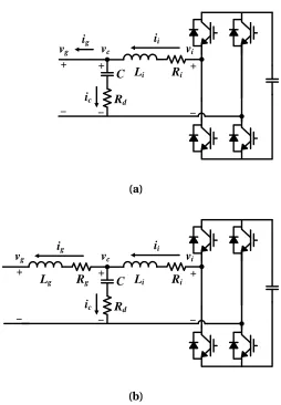
Figure 2.3Circuit diagram of voltage source inverter (VSI) for single-phase system. (a) LC-filtered
VSI. (b) LCL-filtered VSI.
feasible and thus, is widely being used for the UPSs. Today it is extending its range of
application to the DG systems to increase the reliability of the microgrid. When the droop
method is used in the grid-connected converters, the capacitor voltage of the input filter of
the converters are controlled instead of the speed and the back-EMF of the synchronous
single-phase power system, LC-filtered and LCL-filtered voltage source inverter (VSI). The higher
order input filters have better performance than the L-filter in preventing the harmonic
current of switching-frequency level polute the grid. In addition, the total inductance can
be reduced compared to the L-filter, which results in the reduction of the volume, weight,
and cost of the input filter[41],[42]. Other advantage of using LC or LCL filter is that the capacitor voltage can be used as a voltage source, e.g. a generator. Thus, LC or LCL-filtered
VSI are used for not only the dynamic voltage restorer (DVR) but also the DG generating
units with droop method.
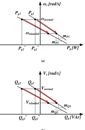
Fig. 2.4 shows the conventional droop method which is applied to the LC or LCL-filtered
grid-connected converters. Each figure has two different droop curves which are for two
converters operating in parallel. Fig. 2.4a shows the relationship between the frequency of
the capacitor voltage and the active power which each converter provides to the load. The
droop characteristic is determined by the normal operating point,Pg∗, and the droop slope,
mP. When the microgrid is islanded, the frequency of the capacitor voltage is dropped and
converged to a value,ωi s l a n d e d, according to the droop characteristic of the two converters. The droop curve should be determined considering the power sharing of the two
convert-ers. Fig. 2.4b shows the relationship between the magnitude of the capacitor voltage and
the reactive power of the two converters. The droop characteristic is determined by the
normal operating point,Qg∗, and the droop slope,mQ, like the droop curve in Fig. 2.4a. The
manitude of the capacitor voltage is dropped when the microgrid is islanded. It can be seen
that the converters mimick the operation of the synchronous generators by applying the
droop method to the capacitor voltage of the input filter.
P
g[W]
ω
c[rad/s]
m
P1ω
normalω
islandedP
g1P
g2P
g1*P
g2*m
P2(a)
Q
g[VAr]
V
c[rad/s]
m
Q1V
normalV
islandedQ
g1Q
g2Q
g1*Q
g2*m
Q2(b)
Figure 2.4Conventional droop method. (a) frequency droop method. (b) magnitude droop
above, the reference of the frequency of the capacitor voltage is calculated by the “real
power versus frequency (P-ω)" droop control, and the reference of the magnitude of the
capacitor voltage is calculated by the “reactive power versus voltage (Q-E)" droop control
[34]. The droop characteristic can be expressed as
ωc∗=ωg+mP(Pg∗−Pg) (2.4)
Vc∗=Vg+mQ(Qg∗−Qg) (2.5)
where theωg and theVg denote the frequency and magnitude of the grid voltage,
repec-tively, calculated by phase- locked loop (PLL). These value can be replaced with any fixed
dispatched value. If the PLL value is used, any fixed value should replace those when the
microgrid is islanded.
The droop control enables the power sharing of the converters connected in parallel.
In addition to the power sharing, the microgrid can operate in the autonomous islanding
mode without any wireless communication among the converters. However, if there is a
wide variation of the power during the grid connected operation such as the SST, the droop
characteristic changes and the power is shared in unexpected way when the microgrid is
islanded. For example, in Fig. 2.4a, if the second converter draws more power from the grid,
which meansPg2∗decreases, its droop curve shifts to the left side of the graph. It means
that the amount of power the second converter is supposed to provide for the islanding
operation is decreased. If the first converter cannot afford to compensate the decreased
amount, the autonomous islanding fails. One possible way to solve this problem is to
adjust the droop slope according to the change of the power during the grid-connected
Pg_max
-Pg_max
Pg [W] ωc [rad/s]
ωc_max
ωc_min
Qg_max
-Qg_max
Qg [VAr]
Vc [V]
Vc_max
Vc_min
mP
mQ
Pg , Pg*
v
gPLL
ω
gmP
ωc*
θc*
Qg , Qg*
VC*
mQ
vc*
* *
( )
c g m PP g Pg
* *
( )
c g Q g g
V V m Q Q
1
s * * *
cos( )
c c c
v V
V
gFigure 2.5Block diagram of the conventional droop controller.
the wide variation of the operating point. Moreover, it is still difficult to estimate the exact
amount of the power to be shared among the converters if the operating point of each
converter is deviated from the normal point. The autonomous islanding is not guaranteed.
As shown in Fig. 2.5, the droop controller determines the reference of the capacitor
voltage of the LC or LCL filter. Therefore, a capacitor voltage controller is needed to
synthe-size the reference voltage. Typically, the LC filter is used to regulate the capacitor voltage,
autonomous islanding is not the requirement of the system, the LCL-filtered converter is
controlled by a typical grid current controller. On the other hand, the LCL-filtered converter
is controlled by the capacitor voltage controller if the autonomous islanding operation is
needed.
The most widely used compensator for the grid-connected converter is the
propor-tional+resonant (PR) controller. As mentioned previously, it is used in the stationary ref-erence frame. While the synchronous PI controller is designed in the synchronousd-q
reference frame by transforming the stationary variables to thed-qvariables, the PR
con-troller can be directly designed in the stationary reference frame with the same steady
state and transient performance as the synchronous PI controller. The PR regulator can be
expressed as
G =KP+
2KIωcs
s2+2ω
cs+ωf2
(2.6)
whereωf is the system fundamental frequency, ωc is cutoff bandwidth,KP is the
pro-portional gain andKI is the integral gain. The resonant controller is used to control the
fundamental frequency component by setting theωf as the system fundamental frequency. It can be used to control the current or voltage at the frequency of interest and thus,
low-order harmonic components of the current or voltage can also be regulated by using the
resonant controller, which is called the harmonic compensator (HC). The HC is expressed
as
Gh=
X
h
2KI hωc hs
s2+2ω
c hs+ωh2
P
g*Droop
Controller
v
c*G
outerPWM
v
i *v
cP
gGating
v
iQ
g *Q
gG
inneri
inneri
inner*v
cv
gv
PCCFigure 2.6Block diagram of the multiloop controller of the LCL-filtered converter.
whereωh is the low-order harmonic frequency,ωc h is cutoff bandwidth for the harmonic
frequency,KI his the integral gain for the harmonic frequency. The HC for each low-order
harmonic frequency can be added in parallel with the PR controller for the fundamental
frequency. Since the resonant regulator provides harmonic compensation functionality,
the PR controller is preferred to the synchronous PI controller when the converter is used
with the grid, especially with the single-phase grid.
The typical structure of the controller of the LCL-filtered converter is shown in Fig. 2.6.
As shown above, the outer loop and the inner loop are used, which is called multiloop
controller. The outer loop controls the capacitor voltage of the LCL filter. It is for reference
tracking performance at steady-state[22]. The outer loop compensator can be expressed as
Go u t e r=KP v+
2KI vωc vs
whereωf is the system fundamental frequency,ωc v is cutoff bandwidth,KP v is the
propor-tional gain andKI vis the integral gain. The inner loop regulates either the capacitor current
or the converter current. The role of the inner loop is to improve dynamic performance of
the system and to provide damping effect. Therefore, only a proportional controller is used
Gi n n e r =KP i (2.9)
whereKP i denotes the proportional gain.
A major challenge of the droop method is the coupling of the active and reactive power.
It is due to the high resistance of the cable used in distribution level or residential level. The
cable used in transmission level is mainly inductive. However, in the distribution level or
the low voltage level, the resistance of the cable is not ignorable and thus, the active and
reactive power is coupled. This power coupling affects the accuracy of the power control
and may induce the oscillation of the power. A rotational transformation is proposed in
[37]to decouple the active and reactive power by using the ratio between the resistance and the reactance of the cable. However, it is hard to be used for the power sharing of the
parallel converters when islanded.
A virtual impedance method is another solution for the power decoupling[12],[23], [43]. It is to add virtual impedance, which is mainly inductive, between the grid and the capacitor of the input filter of the converter to make the cable more inductive. Fig. 2.7 shows
a block diagram of the virtual impedance implementation technique presented in[12]. The virtual resistanceRv and the virtual inductanceLv are implemented by subtracting
the voltage across the virtual impedancevvαβfrom the reference of the capacitor voltage
Droop
Controller
v
c*Virtual Impedance
-
ω
L
vω
L
vR
vR
vi
αi
gαβi
βv
αv
βv
vαβP
gQ
gv
cG
outerFigure 2.7The virtual impedance implementation technique.
inductance jωLvig, considering only the virtual inductance at the fundamental frequency.
The implementation in the box of Fig. 2.7 comes from the stationary reference frame
derivation,vα+j vβ = jωLv(iα+j iβ) =ωLv(−iβ+j iα). In[23], another implementation
technique is presented which can cover not only the fundamental frequency but also
the low order harmonic frequency of interest. However, a proportional gain is ignored to
prevent a differentiation term from amplifying high-frequency noise, which may degrade
the accuracy of the fundamental frequency controller.
2.2
Active synchronization methods and seamless
reconnec-tion of microgrid
Fig. 2.8 shows the DG microgrid connected to the utility at the PCC through a static transfer