Low Power and Area Efficient Static
Differential Sense Amplifier Shared Pulse
Latch
S.Nagakumararaj,S.Vimal raj
Assistant Professor, Dept. of EEE, Sri Krishna College of Technology, Coimbatore, Tamilnadu, India
ABSTRACT: In this project, a low power and low area shift register using pulsed latch has been analyzed. The timing elements and clock interconnection networks such as flip-flops and latches are one of the most power consuming components in modern very large scale integration (VLSI) system. The area, power and transistor count has been compared and designed using several latches and flip-flop stages. The conventional shift register uses Adaptive coupling flip-flop (ACFF) which is used to store the binary data information consumes more power and area. To overcome this problem, we go for Static differential sense amplifier shared pulse latch (SSASPL) which saves more area and power compared to the conventional shift register with flip-flops. A 5-bit shift register using pulsed latch has been designed using pipe logic and fabricated using an IBM 180nm technology. The proposed shift register saves 90% power compared to the conventional shift register with flip-flops.
KEYWORDS: Pulse triggered Latches, Flip Flop, Shift Registers and Pipe Logic.
I. INTRODUCTION
In many digital very large scale integration (VLSI) designs, the clock system that includes clock distribution network and flip-flops is one of the most power consumption components. It accounts for 30% to 60% of the total system power, Where 90% of which is consumed by the flip-flops and the last branches of the clock distribution network that is driving the flip-flop. To achieve a design that ensures both power consumption and small latency is essential in modern VLSI technology. The dual-edge triggering is an important technique to reduce the power consumption in the clock distribution network. By utilizing dual-edge triggering, the flip-flop is capable of sampling data on both rising and falling edges of the clock so that only half the clock frequency is needed to obtain the same data throughput of single edge-triggered flip-flops (SETFFs). Recently, several low-power high-speed DETFF structures have been proposed .In this work, we extensively studied the operation of existing flip-flop architectures, analyzed their weaknesses and proposed new sense-amplifier based flip-flop circuits (herein after, referred to as a “SAFF” circuit) due to its differential characteristics, fast operation speed, and low-power consumption. This SAFF circuit is implemented by various approaches within digital circuits such as microprocessors, digital signal processing units, and the like. The first flip-flop achieves substantial power reduction by concurrently incorporating dual-edge triggering and conditional pre-charging. It also minimizes the latency by making use of a fast symmetrical latch. The proposed design promises an even greater amount of power savings.
II. RELATED WORK OPERATION OF ACFF
Latches are the sequential circuit which shows transparent behavior i.e. the possible changes of the input value can be transmitted to the output. Whereas, in FFs circuit applying the change in input value and change in the output are two separate operations. The FF is designed using MSL. The MSFF is designed with system integrity through redundancy. The MSFF with edge trigger clock signal design with two latches and one inverter. The Master latch performs basic binary storage operation and drives the second latch, the slave by transmitting the binary output of master. The inverter connects the complemented clock signal of master latch to the clock signal of slave latch as shown in Fig 3.1. The clock signal at master act as a switch: when the signal is activated i.e. clk =1 then switch activates and input signals can enter in master, but when the signal is inactivate i.e. clk= 0 then the switch is off and no input signal can enter. The inverter working will not allowed to master and slave FFs cannot be operate at the same time, rather, when clk=1, the other must perforce be close. This one switch turn on at a time technique minimizes the effect of erroneous inputs on the outputs of the circuit.
Fig 2.1 Master Slave Latch(MSL)
When the clk=1, the switch to the master opens the path of master input, thus output of the master latch is controlled by the input signals. At the same time, the input path of the slave latch is disconnected, this disabled the slave latch and any change in master output will not affect the slave output. When the clk=0, the input path of master is disconnected and the input path to the slave is open. At the same time, the master latch can drive the slave latch forcing the slave’s output binary data to equal the master’s output.
The Bistable Cross-coupled Dual Modular Redundancy ACFF on 180nm technology. It works with the single-phase clock design by pass-transistors. The power dissipation is reduced without using local clock buffers. As data activity becomes low, total power dissipation is drastically reduced. Fig 3.1 shows the modified standard dynamic C²MOS master slave latch that has shown good low power features, like small clock load and low power feedback.
The Adaptive Couple (ACFF) Flip-flop works when the stored value Q is changed from 0 to 1. In the conventional FFs, the power dissipation of clock buffers is dominant if is low. The AC elements as shown on the Fig 3.2 composed of a CMOS pass gate are required to overwrite the master latch connected to the input inverters through PMOS pass transistors. They weaken the connection between the cross coupled inverters when the input and overwritten values are different. This fig explains how the AC element works when changing the stored value (Q) from 0 to 1. After CLK becomes low, the nodes N2 and N3 should change the stored values. The two AC elements AC0 and AC1 promote these value changes by turning off appropriate MOS transistors. The NMOS transistor in turns off in AC1 order to assist N3 to flip from 0 to 1. Without the AC elements, the output of cross-coupled inverters prevents these two nodes to flip. When the master latch value is transferred to the slave latch, the AC elements isolate the cross-couple connection in the master latch to make it easier for the master latch to overwrite the slave value.
The TG based master-slave FF using 180nm technology is shown in fig 3.3. For the large output load the charging and discharging of output capacitance, thus delay increases. In static CMOS delay depends on R (resistivity) which is inversely proportional to the width of the transistor and c (capacitance) which is proportional to the size of the transistor in the next stage. Hence by increasing the channel width of the transistor, speed will be increased since there is more space for the current to flow and it is called as Transistor sizing. The fig shows master-slave latch with two transmission gates, four PMOS, four NMOS and three inverter logic. Its main advantage is the short direct path and the low power feedback.
Fig.2.3 Transmission Gate base shortest path Feedback FF.
2.1 AREA CALCULATION:
Number of transistors in one bit shift register = 07
Therefore number of tansistors in 5 bit shift register = 07 X 5= 35 Area = 35 X 180nm2
= 6300nm2
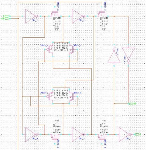
III. PROPOSED WORK OPERATION OF SSASPL
Fig:3.1 Schematic diagram of SSASPL
The proposed shift register uses latches instead of flip flops to reduce the area and power consumption.
The SSASPL (static differential sense amp shared pulse latch) in Fig. 2, which is the smallest latch, is selected. The original SSASPL with 9 transistors is modified to the SSASPL with 7 transistors in Fig. 2 by removing an inverter to generate the complementary data input (Db) from the data input (D). In the proposed shift register, the differential data inputs (D and Db) of the latch come from the differential data outputs (Q and Qb) of the previous latch. The SSASPL uses the smallest number of transistors (7 transistors) and it consumes the lowest clock power because it has a single transistor driven by the pulsed clock signal. The SSASPL updates the data with three NMOS transistors and it holds the data with four transistors in two cross-coupled inverters. It requires two differential data inputs (D and Db) and a pulsed clock signal. When the pulsed clock signal is high, its data is updated. The node Q or Qb is pulled down to ground according to the input data (D and Db). The pull-down current of the NMOS transistors must be larger than the pull-up current of the PMOS transistors in the Inverters.
The output signals of the first latch (Q1 and Q1b) change correctly, because the input signal of the first latch (IN) is constant during the clock pulse width. On the other hand, the output signals of the second latch (Q2 and Q2b) do not change, because the input signals of the second latch, which are connected to the output signals of the second latch (Q2 andQ2b), change during the clock pulse width. The SSASPL flips the states of the cross-coupled inverters (Q and Qb) by pulling current down through either NMOS1 or NMOS2 during the clock pulse width. The clock pulse width is selected as the minimum time to flip the output signals of the latch (Q and Qb) when its input signals (D and Db) are constant. If the input signals change during the clock pulse width, the time pulling current down through either NMOS1 or NMOS2 becomes shorter than the clock pulse width, so that the latch has not enough clock pulse time to flip the output signals after the input signals change. The sequence of the pulsed clock signals is in the opposite order of the latches. Each latch has a constant input during its clock pulse so there is no timing problem.
A. AREA CALCULATION
Number of transistors in one bit shift register = 07
Therefore number of tansistors in 5 bit shift register = 07 X 5= 35 Area = 35 X 180nm2
= 6300nm2
PIPE LOGIC
current state as bits in some kind of memory. A convenient type of memory is the D-flip flop. It can be implemented in a number of ways, and we'll go for a variant that uses TSPC (true single-phase clocked) logic. This design is interesting because it relies on the parasitic capacitance of the wires, so when used in a real integrated circuit it requires a minimum clock frequency to work, otherwise the bits stored in the registers become corrupt through leakage currents. Our pipe capacitors are ideal in the sense that there's no leakage at all. The buffers hold their contents until the pipe is destroyed .In a digital system, synchronization/clocking has its special role. By its action as timing signal the system clock controls the working rhythm of the chip. If the system is considered as a set of interconnected gates and flip-flops, the clock signal controls all flip-flops to sample and store their input data synchronously. Therefore, the clock signal tends to be highly loaded. In addition, to distribute the clock and control the clock skew, one needs to construct a clock network (often a clock tree) with clock buffers .All of this adds to the capacitance of the clock net which also happens to have the largest activity (2 transitions per cycles) in a synchronous circuit (ignoring possible hazard activity on same signal lines).
Recently the clock signals in digital computers consume a large (15% - 45%) percentage of the system power. Thus, reducing power dissipation due to the clock net is an important task in LSI designs, such as the wireless communication system clock is only 50%. Low and high levels of the clock signal put a latch in either a storage state or an input state.
Fig.4.1 Schematic diagram of pipe logic
In the storage state, the clock level switches off the input path, the input data is thus rejected, while in the input state, the clock level allows the input signal to travel to the output terminal of the latch. However, if input date can be received and sampled at both levels of the clock, the flip-flop will receive and process two data values in one clock period. In other words, the clock frequency could be reduced by half while keeping the data rate the same. This means that under the requirement of preserving the original circuit function and data rate, the dynamic power dissipation due to clock transitions can be reduced by half. It is expected that the half-frequency reduced clock system is useful in low power systems (including wireless, battery operated systems).
A. AREA CALCULATION
Number of transistors in one bit shift register = 10
Therefore number of tansistors in 5 bit shift register = 10 X 5= 50 Area = 50 X 180nm2
IV. SIMULATION RESULTS
.
Fig.2.4. Output waveform for ACFF
Fig:4.2 Output waveform of 5-bit pipe logic
V. CONCLUSION AND FUTURE WORK
The area, power and transistor count has been compared and designed using several latches and flip-flop stages. This proposed Static differential sense amplifier shared pulse latch (SSASPL) saves more area and power compared to the conventional shift register with flip-flops. This proposed shift register saves 50% area and 90% power compared to the conventional shift register with flip-flops using tanner tool IBM 180nm technology.
This project can be extended by using tanner tool IBM 90nm technology on above shift register to get reduced area when compared with the proposed shift register. Tanner tool IBM 90nm technology reduces the transistor size which ultimately reduces the area and power consumed.
REFERENCES
1. “Low-Power and Area-Efficient Shift Register Using Pulsed Latches”, Byung-Do Yang ,IEEE TRANSACTIONS ON CIRCUITS AND SYSTEMS—I: REGULAR PAPERS, VOL. 62, NO. 6, JUNE 2015
2. “Low Power Pulse-triggered Flip-flop Design Based On A Signal Feed-through Scheme”, Jin-fa lin, IEEE TRANSACTION ON VERY LARGE SCALE INTERGRATION(VLSI) SYSTEM,VOL 22,NO.1,JANUARY 2014.
3. “Design and Analysis of Explicit Pulse Triggered Flip- Flops using PTL based AND gate”, V.Vijaya ratina, INTERNATIONAL JOURNAL OF ELECTRONICS AND MODERN TECHNOLOGY, VOL-01, ISSUE-02., APRIL-2015.
4. “Design of a Low-power Efficient Double Edge Trigger Flip-flop”, R.Sivakumar, INTERNATIONAL JOURNAL OF ELECTRONICS AND MODERN TECHNOLOGY, VOL.3, NO.6, JUNE 2015.
5. “ Power- Efficient Explicit –Pulsed Dual –Edge Triggered Sense- Amplifier Flip –Flops”, Myint-Wai-Phyu, IEEE TRANSACTION ON VERY LARGE SCALE INTERGRATION(VLSI) SYSTEM,VOL 19,NO.1,JANUARY 2011.
6. “low power and high performances flip-flops”, Natasha, INTERNATIONAL JOURNAL OF SCIENCE, ENGINEERING AND
7. “A Reduced Clock-Swing Flip-Flop (RCSFF) for 63% Power Reduction”, Hiroshi Kawaguchi, IEEE JOURNAL OF SOLID-STATE CIRCUITS, VOL. 33, NO. 5, MAY 1998
8. Y. Ueda et al., “6.33 mW MPEG audio decoding on a multimedia processor,” in IEEE Int. Solid-State Circuits Conf. (ISSCC) Dig. Tech. Papers ,Feb. 2006, pp. 1636–1637
9. B.-S. Kong, S.-S. Kim, and Y.-H. Jun, “Conditional-capture flip-flop for statistical power reduction,” IEEE J. Solid-State Circuits, vol. 36, pp. 1263–1271, Aug. 2001.
10. C. K. Teh, T. Fujita, H. Hara, and M. Hamada, “A 77% energy-saving 22-transistor single-phase-clocking D-flip-flop with adaptive-coupling configuration in 40 nm CMOS,” in IEEE Int. Solid-State Circuits Conf. (ISSCC) Dig. Tech. Papers, Feb. 2011, pp. 338–339.
BIOGRAPHY