CMOS Half Adder Design & Simulation Using Different Foundry
Shital Baghel1, Pranay Kumar Rahi2, Nishant Yadav31M.Tech Scholar, 2M.E Scholar, 3M.Tech Scholar
1Department of Electronics &Electrical Engineering, Indian Institute of Technology Kharagpur, India
2
Department of Electronics & Communication Engineering
National Institute of Technical Teachers’ Training & Research, Chandigarh, UT, India 3Department of Computer Science and Engineering, Indian Institute of Technology Kharagpur, India
ABSTRACT
Adders are used in processors in the arithmetic logic units, to calculate addresses, table indices, and other similar operations. A fast and energy-efficient adder plays a vital role in electronics industry. Adder contributes substantially to the total power consumption of the system. Half Adders are frequently required in VLSI from processors to application specific integrated circuits (ASICs). In this paper, proposed 1-bit half adder is simulated which is then analyzed and comparison has been done on account of the power and surface area. The simulations in 90nm, 70nm and 50nm CMOS technologies were done. The half adder using 50nm CMOS technology is better in terms of power and surface area as compare to 90nm and 70nm CMOS technologies.
KEYWORDS: CMOS, VLSI, Half adder, Power consumption, CMOS technology.
1.
INTRODUCTION
Adder circuit is a combinational digital circuit that is used for adding two numbers. A typical adder circuit produces a sum bit (denoted by S) and a carry bit (denoted by C) as the output. Typically adders are realized for adding binary numbers but they can be also realized for adding other formats like BCD (binary coded decimal, XS-3 etc. Besides addition, adder circuits can be used for a lot of other applications in digital electronics like address decoding, table index calculation etc.For more than four decades, downscaling of CMOS has been the fundamental strategy for improving the performance of VLSI circuits. However, there have been reports suggesting that the MOS transistor cannot shrink beyond certain limits dictated by its operating principle [1].The speed and power dissipation are the important parameters which should be taken into consideration in digital circuits. In order to achieve energy efficient and low power VLSI
(Very Large Scale Integration) circuits, a novel adder using XOR gates which are in turn designed with less number of transistors is implemented. Modification of XOR gate portion in an adder using minimum number of transistors is the key idea for the design [2]. XOR gates are the most fundamental blocks for building adder systems [3]. The performance of adder can be improved by designing XOR gate such as using minimum number of transistors but without sacrificing the performance. XOR gates were designed using eight transistors or six transistors in early designs [4].Since number of integrated transistors become double in once in 18 months, there is a much need to fabricate low power VLSI chips. Portable consumer electronic products powered by batteries is an another factor for low power VLSI Design, since the battery technology alone cannot solve the low power problem [5].
2. EFFICIENT HALF ADDER DESIGNS
In DSPs, and, versatile microprocessor, the wide-bit addition is vital in many applications such as ALUs,
multiply-and accumulates (MAC) units. The half
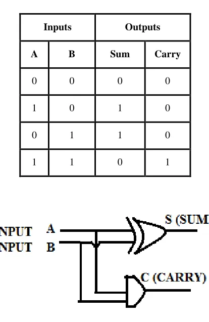
adder adds two single binary digits A and B. It has two outputs, sum (S) and carry (C). The carry signal represents an overflow into the next digit of a multi-digit addition. The value of the sum is A+B. The simplest half-adder design incorporates an XOR gate for S and an AND gate for C. With the addition of an OR gate to combine their carry outputs, two half adders can be combined to make a full adder. The half adder adds two input bits and generates a carry and sum, which are the two outputs of a half adder. The input variables of a half adder are called the augend and addend bits. The output variables are the sum and carry as shown in figure 1. The truth table for the half adder is:
Table 1. Truth table of 1-bit half adder
Inputs Outputs
A B Sum Carry
0 0 0 0
1 0 1 0
0 1 1 0
1 1 0 1
Figure 1. Simple half adder using XOR and AND gate.
NAND gates or NOR gates can be used for realizing the half adder in universal logic and the relevant circuit diagrams are shown in the figure 2(a) and figure 2(b).
Figure 2(a) Half adder using NAND logic
Figure 2 (b) Half adder using NOR logic
2.1
Power Delay Product in Logic Gate
The power–delay product in digital electronics is a figure of merit correlated with the energy efficiency of a logic family or logic gate. It is the product of power consumption (averaged over a switching event) times the input–output delay, or duration of the switching event and is also known as switching energy. It has the dimension of energy, and measures the energy consumed per switching event.
2.2 Power Dissipation in CMOS
Dynamic dissipation and short circuit are the component of power to be considered during the input signal transition. To modify the charge content of the capacitive load, the dynamic power is dissipated and it is proportional to the switching frequency and to the load capacitance, and also depends on the area of the buffers. By the simultaneous conduction of P and N transistors during the transition of the input signal the short circuit power dissipation is produced. The ratio of input to transition times is a good indicator of short circuit power dissipation. The value of ratio should be comparable or lower than unity, and it is the objective of buffer design, the short circuit power dissipation can be omitted. In the result just consider the dynamic component to optimize objectives. The total value of the load capacitances includes layout parasitic (diffusion and interconnect) and active loads is the minimum capacitance [6].
3.
SIMULATION AND RESULTS
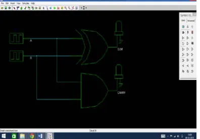
The 1-bit half adder are compared based on the performance parameters like surface area and power dissipation. To achieve better performance, the circuits are designed using CMOS process by Microwind 3.1 in 90nm, 70nm and 50 nm technology. The proposed 1-bit half adder circuit shown in figure 3, uses 2-bit X-OR and 2-bit AND logic gates. All the layouts and simulation results presented here are done in Microwind3.1 which is a layout editor and simulator. On the layout presented by this tool, simulation can be done. Simulation is first performed using schematic entry and its corresponding test patterns are generated and is verified whether it is functioning properly or not. The schematic file after verification is converted to VERILOG file. Then the VERILOG file is imported using the command “compile Verilog file” using MW environment so that the schematic of the logic design will be converted into physical layout. MSK File is used to store the information of the layout design. Power dissipation, rise delay, fall delay, timing
results, layout area are the performance
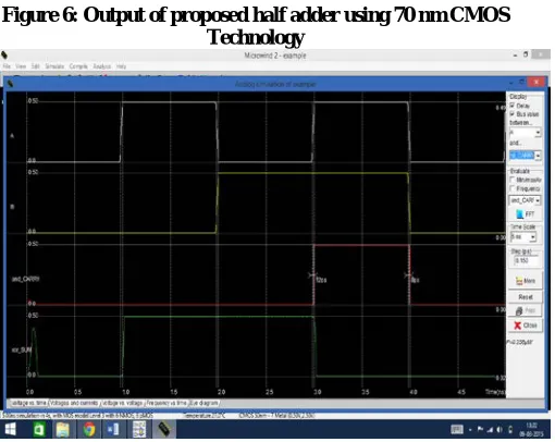
characteristics which can be provided by this tool. There is a facility in this tool to convert layout to Caltech Intermediate Format (CIF) which provides the information for fabrication. To extract the electrical parameter there is a program EXTRACT in this tool. Metal Oxide Semiconductor Implementation Service (MOSIS) uses standard mask layout like CIF for fabrication. Figure 5-7 shows the timing diagram results of proposed 1bit half adder using 90nm, 70nm, 50nm CMOS fabrication technology.
Figure 3: Schematic design flow of proposed half adder
Figure 4. Layout design of proposed Half Adder
Figure 5. Output of proposed half adder using 90nm CMOS Technology
Figure 6: Output of proposed half adder using 70 nm CMOS Technology
Figure 7. Output of proposed half adder using 50 nm CMOS Technology
The comparative results for proposed 1-bit half adder for 90nm, 70nm and 50 nm CMOS design technology are given in Table-2.
Table 2. Power and surface area analysis of 1-bit Half adder in different CMOS technologies
CMOS Technology
Parameters
90 nm 70 nm 50 nm
Power
(in µW) 5.150 1.690 0.258
Surface Area
( in µW2) 26.500 13.000 6.600
4. CONCLUSION
The proposed 1-bit half adder is simulated with 90 nm, 70 nm and 50 nm CMOS technologies .The performance parameters power and surface area are compared. From the results it is found that the power and surface area has been improved by 67.15% and 50.94% respectively for proposed 1-bit adder using the proposed logic in 70nm CMOS technology. Finally an improvement of 94.99%
and 75.09% for proposed 1-bit adder were found using the proposed logic in 50nm CMOS technology.
REFERENCES
[1] Y.Tau, D.A.Buchanan, W.Chen, D.Frank, K.Ismail, S.Lo, G.Sai-Halasz, R.Viswanathan, H.Wann, S.Wind, and H.Wong, “CMOS Scaling into the Nanometer Regime,” Proceeding of the IEEE, vol.85, pp. 486–504, 1997.
[2] V. Elamaran, G. Rajkumar, S. Singh Rajpurohit and R. Anooj Krishnan, 2014. “Low Power Adder-Subtractor using Efficient XOR Gates.” Journal of Applied Sciences, 14:
1623-1627.
[3] Haghparast, M. and K. Navi, 2007, “Reversible full adder circuit for nanotechnology based systems” J. Applied Sci., 7: 3995-4000.
[4] Leblebici, Y. and S.M. Kang, 1999. “CMOS Digital Integrated Circuits”. 2nd Edn. McGraw Hill, Singapore. [5] Yeap, G.K., 1998. “Practical Low Power Digital VLSI
Design” Kluwer Academic Publishers, Norwell, MA., ISBN: 0792380096, Pages: 233.
[6] T.Thirumurugan , J.Sathish Kumar,2012, “Energy Efficient Implementation for Arithmetic Application in CMOS Full Adders” International Journal of Computer Applications (0975 – 8887) Volume 57– No.2, November 2012
AUTHORS
Shital Baghel received the Bachelors of Technology degree in Electronics and Telecommunication Engineering from CSIT Durg, Chhattisgarh Swami Vivekananda Technical University, Bhilai, Chhattisgarh,
India in 2009, and pursuing Masters of Engineering in Electronics and
Communication Engineering from Indian Institute of
Technology Kharagpur, India.
Pranay Kumar Rahi received the
Bachelors of Technology degree in
Electronics and Telecommunication Engineering from Government Engineering College, Guru Ghasidas University, Bilaspur, Chhattisgarh, India in 2004, and pursuing Masters of Engineering in Electronics and Communication Engineering from National Institute of Technical Teacher’s Training & Research, Punjab University, Chandigarh, India.
Nishant Yadav received the Bachelors of Technology degree in Computer Science and Engineering from Government Engineering College, Guru Ghasidas University, Bilaspur,
India in 2004, and pursuing Masters of Engineering Computer Science and
Engineering from Indian Institute of
Technology Kharagpur, India.