Functional Verification of AMBA AHB LITE
Interconnect using Systemverilog
Pallavi T lambe1, Meghana Kulkarni2
PG Student [VLSI] Dept. ECE, Center of PG studies VTU belagavi, India1
Associate Professor Dept. ECE, Center of PG studies VTU belagavi, India2
ABSTRACT: Verification is the important part of SoC manufacturing, it gives particular implementation and
functionality to DUT for check whether it has achieved specification or not. In this paper communication interconnect i.e. AHB LITE interconnect is verified by developing the reusable verification intellectual property (VIP) using hardware verification language Systemverilog. The AHB LITE is the on-chip-interconnect which manages the functional block in SoC design and develops lossless communication between master and each slave in the SoC design. It also finds the presence of error/bug in the design by generating simulation result and the coverage report using the QUESTA SIM tool.
KEYWORDS: SoC, Systemverilog, AHB LITE, functional verification, QUESTA SIM tool.
I. INTRODUCTION
Due to day by day increase in the complexity of SoC design, verification has become the vital bottleneck in the design technique because it explores correct/incorrect functioning of AHB LITE interconnect in the SoC design. AMBA 3 AHB LITE is the subset of AMBA 2 AHB used in such a SoC design where only one master, one slave or multiple slaves are required like cortex M. There are many approaches of verification of DUT some of these are. In the first approach, the verification of AHB LITE interconnect with wait transfer is carried out and verification environment is developed using UVM methodology. The simulation result of read/write transfer (burst transfer, burst type, burst size) at wait state is explored but coverage report is not covered in verification [1]. In the second approach, the verification of AXI2OCP Bridge is done, which connects two interconnect in SoC design where AXI based processor and the controller based OCP are used [2]. In another approach, the verification of AHB master which is formal based verification but, it is not possible to verify the chip formally because it is math based verification [3].
In this paper Verification IP model is developed and inserted into test bench to simulate and justify the functional correctness of the SoC interconnect (or full SoC design). The simulation result and 100% coverage report of generated test cases using Systemverilog are given.
II.AMBA AHB LITE INTERCONNECT
The AHB LITE is the third version of advanced microcontroller bus architecture (AMBA) introduced by ARM Ltd. Original AHB specification was part of AMBA 2 AHB, some features are removed and named as AHB LITE. The specifications of AMBA 3 AHB LITE are
Support High performance, high clock frequency and high bandwidth operation.
Supports only one master and one or more than one slave.
Separates bus for read and write transfer.
Support pipelined operation, burst transfer.
Support only one master so, no need of arbitration.
No need of master-to-slave multiplexer.
III.AMBA AHB LITE DESIGN
Designing with the AHB LITE interconnect requires the following components: 1. Master
2. Slave
3. Address decoder 4. Multiplexer
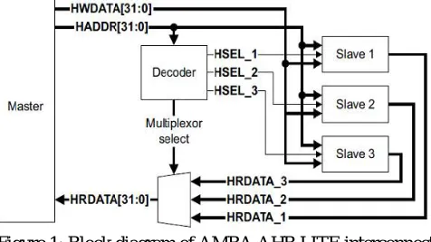
The block diagram for AHB LITE interconnects is shown in Figure 1, with four components i.e.: single master, three slaves, address decoder and slave to master multiplexer. The bus interconnect logic between master to slave consists of one address decoder and multiplexer.
Figure 1: Block diagram of AMBA AHB LITE interconnect
The AHB LITE interconnect supports data bus configuration from 8-bit to 1024-bits but microcontroller supports up to 32-bits data configuration. The 32-bits Address and Control signal sent out of AHB LITE master goes to AHB LITEslave as well as address decoder. Decoder calcifies the transaction to particular AHB LITE slave depending upon the address sent from the AHB-LITE master. Same information is sent to the multiplexer and it will know that which response and data signal mux to the AHB LITE master. At single transfer only one slave will accept the information and other two remains in de-active state. Explanation of each component of Figure 1 is given below:
3.1 AHB LITE Master
The AHBLITE master is the device connected to high throughput bus which gives control and address information to initiate write and read operation. Transfer size of AHB LITE interconnect is fixed which is 32-bits. Figure 2 shows AHB LITE master block diagram which represents the signals of master.
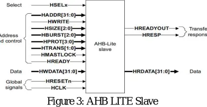
3.2 AHB LITE Slave
The AHB LITE slave is memory component in the SoC design which captures the data, address from the AHB LITE master and reads the data from its memory location. The AHB LITE slave cannot initiate the operation on its own, it only responds to AHB LITE master. The AHB LITE slave receives the signal from AHB LITE master address decoder and sends the transfer response signal and HRDATA to master.
Figure 3: AHB LITE Slave
The AHB LITE slave diagram is shown in Figure 3 which has 32-bit address and control signals from the AHB LITE master and selects signal from the Address decoder and then generates transfer response HREADY, HRESP to AHB LITE master.
3.3 Address decoder
This is the component used when more than two slaves are present in design and it decodes the address of every transfer and gives particular slave signal to AHB LITE slave that is concerned within a transfer. The addresses received from the AHB LITE master are sent to address decoder and particular AHB LITE slave is selected depending on the address coming from AHB LITE master.
3.4 Multiplexer
The multiplexer is used to multiplex the read data and give response signal to AHB LITE master from the AHB LITE slave and also used when number of slave are more than two.
IV. AHB LITE INTERCONNECT VERIFICATION
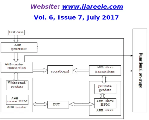
To know about verification environment of AHB LITE interconnect, the testbench architecture must be known in the broader view. The testbench architecture consists of number of elements which are integrated in the proper way to form a verification intellectual property (VIP). The entire verification process is divided into three parts,
1. Test
2. Verification environment 3. Functional verification
The Figure 3 is the architecture block diagram for AHB LITEinterconnects consists of test case, environment and functional verification.
Figure 3: Architectural block diagram for AHB lite interconnect
2) Verification Environment - The verification environment is required to verify the functional correctness of the DUT by driving and creating the input sequence and capturing output of design to compare with golden (expected) output. In the verification environment, separate components are used to perform the specific task and the components are shown in Figure 3.
Generator - Generator generate random testcases and the Systemverilog provide construct to manage random generator order and distribution. These testcases are transferred to the master agent.
Master agent – It is also called as connector/transaction which connects the AHB LITE driver, generator, scoreboard and the functional coverage. It also controls configuration operation of DUT and convert high level information achieved from generator (burst transfer) into the individual command.
Master driver – It gets the data from master agent and drives on DUT by converting into actual input of DUT. It achieves back response from design under test and again converts response in object format to send master agent. The slave agent and slave driver working is same as master agent and master driver.
Scoreboard – It is also known as tracker, consists of reference model in which the expected output is stored. As the random stimuli from generator is sent to DUT and the same stimuli are sent to the scoreboard and saved into DUT till it gives the output. Then the scoreboard compares the actual output and the golden output and gives the result of verification.
3) Functional coverage – It is the one which introduces how much functionality of design is covered. Some features of functional verification are
• Explains which feature in verification checked successfully.
• In verification which part of feature checked and how much it is close to complete verification. • Gives confidence that the previously fixed design will not re-produce bugs.
V. SIMULATION RESULT
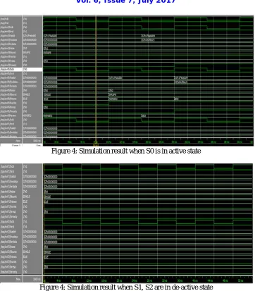
Figure 4: Simulation result when S0 is in active state
Figure 4: Simulation result when S1, S2 are in de-active state
Write operation – The write operation with burst transfer, HREADY signal is high and the HWRITE is also high.The
Figure 5: Burst write operation
Read operation – After completion of write operation, the read operation will continue with a burst transfer. At read
transfer the HREADY is high and HWRITE is low as shown in below Figure 6.
Figure 6: Burst read operation
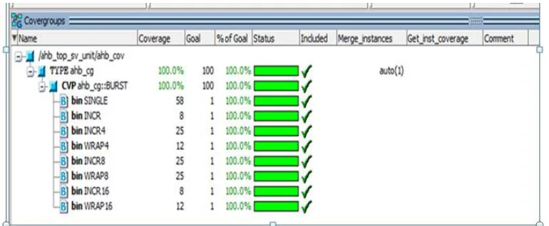
Coverage report – The 100% coverage report for AHB LITE interconnects is shown in below Figure 7 which covers
VI.CONCLUSION
In this paper, code for AHB LITE interconnect environment is simulated and output is observed. The functional verification of the AHB LITE interconnects, simulation waveforms developed by the Mentor Graphics QUESTA SIM tool and explored as per expectation without any change in the features of DUT.The environment totally wraps DUT under verification and observes the optimum functional, and coverage is functional based coverage.Bins have been created based on the constraints and 100% functional coverage has been obtained on them. The 100% functional coverage report is given by developing the re-usable VIP and by generating the testcases for AHB LITE interconnect. The result is achieved on the latest version of tool i.e., QUESTA SIM 64 10.C tool.
REFERENCES
[1] “M.B.R.Srinivas and Sarada Musala”, “Verification of AHB_LITE protocol for waited transfer responses using re-usable verification methodology.” 2016 IEEE.
[2] “Golla Mahesh, and Sakthi vel.SM”, ” Functional Verification of the Axi20cp Bridge using System Verilog and effective bus utilization calculation for AMBA AXI 3.0 Protocol.” 2015 IEEE.
[3] “Nguyen Son Lam and Nguyen Due Minh”,”ARB-Master Controller Formal Compliance Verification.” 2014 IEEE.
[4] “Ashutosh Kumar Singh, Anurag Shrivastava and G.S. Tomar”, “Design and Implementation of High Performance AHB Reconfigurable Arbiter for On chip Bus Architecture.” 2011 IEEE DOI 10.1109/CSNT.2011.99
[5] “Purvi D. Mulani”, “SoC Level Verification using System Verilog.” 2009 IEEE.
[6] “Han Ke1 Deng Zhongliang1 Shu Qiong2”, “Verification of AMBA Bus Model Using System Verilog”. IEEE 2007.
[7] “Asharani Pattedar andSaroja V. Siddamal”, “Design and Verification of AMBA 3 AHB Lite Protocols by using GO2UVM Package.” IJET 2016
[8] “Sravya Kante, Hari Kishore Kakarla and Avinash Yadlapati”, ” Design and Verification of AMBA AHB Lite protocol using Verilog HDL” 2015 IJET.
[9] “Han Ke1 Deng Zhongliang1 Shu Qiong2”, “Verification of AMBA Bus Model Using System Verilog”. IEEE 2007.
[10] “Pradeep S R1, Laxmi C2”, “DESIGN AND VERIFICATION ENVIRONMENT FOR AMBA AXI PROTOCOL FOR SOC INTEGRATION” 2014 IJET.
[11] “Deepika ahlawata and Neeraj Kr.shukla”, “DUT verification through an efficient and reusable environment with optimum assertion and functional coverage”