1461 | P a g e
PERFORMANCE EVALUATION OF
DIFFERENTREAD PORTS IN STATIC RANDOM
ACCESS MEMORY IN 45NM CMOS TECHNOLOGY
Kirti Gupta
Dept. of Electronics and Communication, Bharati Vidyapeeth’s
College of Engineering, New Delhi (India)
ABSTRACT
The Static Random Access Memory (SRAM) has one of the most critical roles in modern computer architecture designs. The SRAM consists of an array of bit cells, each of which can store one bit of information. The performance of entire SRAM depends upon the ability of an individual cell’s read and write operation. It is therefore imperative that each cell is able to perform a read operation quickly and correctly evaluate values. The read port in SRAM cells suffers from design issues such as evaluation speed, area, leakage current and bit line offset. The problems are only worsened due to process, voltage and temperature variations. In this work, a comprehensive evaluation of SRAM read ports on the basis of bit line offset, size, capacitance, read current and leakage current on the 45nm CMOS Technology has been presented. The results showed that the conventionally used 6T SRAM cell had the highest leakage current, the highest bit-line offset and overall lowest performance. The 8T cell showed moderate performance metrics. However, the 8T cell with modified read port showed the lowest bit line offset, lowest leakage current and the lowest capacitance. These performance metrics directly translated to higher read operation performance in SRAM.
Keywords
:
6T Cell, Leakage Current, Read Bit Line, Voltage Offset, SRAM
I. INTRODUCTION
The SRAM is a high-performance memory used in cache in microprocessors and system-on-chip devices. It
occupies a large portion of the any processor and has a direct impact on the performance of the microprocessor
[1]. Since there has been a need for battery powered portable devices in the recent times, the memory ought to
be highly efficient in terms of power consumption. This places a design constraint on the power consumption of
memory. These portable devices also require large amount of computing power which in turn requires a
high-performance cache memory.The designer thus has to be meticulous about the high-performance and power trade-off
when designing SRAMs.
The most commonly used SRAM bit cell is the six-transistor cell. It occupies a minimal area, provides
differential sensing and consumes low power. However, there is a design trade-of associated with the 6T SRAM
sub-1462 | P a g e
micron region due to process variations, several alternate designs have been proposed in order to mitigate theperformance issues of the 6T SRAM cell. These attempt to either decouple read and write ports of SRAM cells
or add additional control signals to enhance performance and power consumption at the expense of area.
In this work, different read ports have been compared on the basis of leakage current, bit line offset,
capacitance, and port size. The paper has been constructed as follows. Section II describes the different read port
architectures that are commonly used in SRAM. Section III explains the different performance metric upon
which each port has been evaluated. Section IV shows the simulation results for performance metrics for all the
read ports. Finally, Section V concludes the paper.
II. READ PORT ARCHITECTURES
The SRAM ports can be evaluated on the basis of several design parameters. Each of these design parameters
have been explained in the following sub-sections.
2.1 6T SRAM Cell Port [2]
The six transistor SRAM cell consists of two access transistors (ACL and ACR) for read and write operation, as
shown in Fig. 1. During the read and write operation, the word line (WL) is enabled and the data is received or
put on the bit lines. The internal nodes formed by two cross coupled inverters, store one bit of information. The
cross coupled inverters are formed using two pMOS (Pull Up Left and Pull Up Right) and two nMOS (Pull
Down Left and Pull Down Right). During the standby condition when the cell is not performing any operation, a
static leakage current flows from bit line in to the data node (X). This increases power consumption and
increases the bit line offset. Although the area is very low for such a configuration, the combined pass gate
leakage may inadvertently pull down the bit line in case of larger arrays.
Fig. 1 The conventionally used 6T SRAM Cell using a single nMOS transistor for access port [2]
2.2
8T SRAM Cell Read Port [3]
The eight transistor SRAM cell consists of an isolated read port for noise free read operation. For this operation,
two transistors are used as shown in Fig. 2. In this configuration, the worst-case scenario occurs when the cell
1463 | P a g e
leakage current through the read port. This in turn further increases the bit line offset causing the effective readcurrent to degrade. The resulting performance is worsened due slower sensing speed due to such a sensing
mechanism.
Fig. 3 The 8T SRAM cell with isolated read port using R1 and R2 nMOS [3].
2.3
Modified 8T Cell Read Port [4]
Since the performance of the read port in the 8T cell is degraded, another read port architecture was proposed in
[] as way to mitigate the performance issues of the previous structures. The architecture for this port is shown in
Fig. 3. This involves the replacement of the read operation enable signal to the lower half of the read port. This
effectively reduces the total potential difference between source and drain during hold condition of the SRAM
cell. This causes the subthreshold current to reduce to less than half of original value. The read performance is
greatly increased due to lower bit line offset. The power consumption is also decreased.
Fig. 3 The 8T SRAM cell with modified read port [4].
III. PERFORMANCE PARAMETERS
The SRAM ports can be evaluated on the basis of several design parameters. Each of these design parameters
have been explained in the following sub-sections.
3.1 Leakage Current
The leakage current becomes a greater portion of total power consumption as technology size scales [5]. It
1464 | P a g e
subthreshold current is exponential and dependent on the gate voltage. It is due to carrier diffusion betweensource and drain regions of transistor in weak inversion. The Gate Induced Drain Leakage is part of leakage
current and is caused by high field effect in the drain junction of MOS transistors [6]. This leakage current is
exacerbated by high drain-body potential and high drain-gate potential. Another component of leakage current if
the junction current, flows from high node to substrate. This is also called the Reverse-Diode Leakage because it
flows when the p-n junction between the bulk and drain is reverse biased.
3.2
Read Current
The current that flows during a read operation is known as read current [7]. For the 6T cell, the read current
should be able to pull down the bit line in the required time, while simultaneously not destroying the data in the
cell. For isolated read port cells such as the 8T cell, the effective read current should be as large, so that the read
bit line may be pulled down as quickly as possible for a faster read operation.
3.3
Bit Line Offset
SRAM arrays composed of larger arrays are prone to bit line offset conditions.The combined leakage from all
cells on a column reduces the bit line voltage level. Bit cell pass gate device leakage thus reduces the sense
amplifier input differential due to the subthreshold leakage from the bit lines. The worst-case sensing occurs
when all the unselected bitcells on the column store exactly the opposite data from the selected bit cell. Pass
gate leakage determines the maximum number of bitcells that can be implemented per column. This effect is
usually important in high performance memories due to the low threshold voltage of the pass gate device.
3.4
Capacitance
Larger capacitances not only increase time to charge and discharge nodes during every clock cycle, it also leads
to higher power consumption. This causes issues in heat dissipation as well. Similarly, for SRAM cells, the
capacitance must be as low as possible. This is ensured by smaller vertical sizing for SRAM cells and lower
number of transistors per read port [8].
3.5 Size
Since the area on a chip is expensive, it has to be used judiciously. Therefore, the designer has to be careful
about the size of each cell. A smaller read port in terms of transistor count leads to a smaller SRAM cell. This
causes the overall area of the memory to decrease, thereby lowering the cost [9]
IV. SIMULATION RESULTS
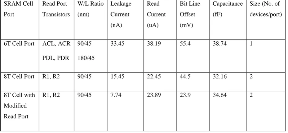
All simulations were performed on the 45-nm CMOS technology [10]. The supply voltage is 0.9V and the
temperature is 27˚C. All read ports were compared on the basis of leakage current, capacitance, bit line offset
and number of transistors per port. The bit line offset was calculated for 128 bit cells per column. The sizing for
1465 | P a g e
TABLE I Performance comparisonSRAM Cell Port Read Port Transistors W/L Ratio (nm) Leakage Current (nA) Read Current (uA) Bit Line Offset (mV) Capacitance (fF)
Size (No. of
devices/port)
6T Cell Port ACL, ACR
PDL, PDR
90/45
180/45
33.45 38.19 55.4 38.74 1
8T Cell Port R1, R2 90/45 15.45 22.45 44.5 32.16 2
8T Cell with
Modified
Read Port
R1, R2 90/45 7.74 23.89 23.9 34.64 2
As shown in TABLE I, the port in 6T cell resulted in the lowest performance of all architectures compared.
With its higher leakage current, the bit line offset also increased. However, it also had the least number of
devices. The read port for the 8T cell showed moderate performance, with low leakage current, lower
capacitance and lower bit line offset. However, the best performance was exhibited by the 8T cell with modified
read port. It had the lowest leakage current, the lowest bit line offset and lowest capacitance. It also showed
good read current performance in comparison to the 8T cell with the same number of transistors per read port.
V. CONCLUSION
In this work, a comprehensive analysis was performed and presented to compare different read ports in SRAM
cells. Each of the port differed in architecture, and performed differently. The most commonly used cells such as
the 6T cell, 8T cell and the 8T cell with modified read port were analysed. The effect of each port on different
performance metric was also discussed. The port ability was explained in correlation with leakage current, read
current, bit line offset, capacitance and number of transistors per port. The results showed that the
conventionally used 6T SRAM cell had the highest leakage current, the highest bit-line offset and overall lowest
performance. The 8T cell showed moderate performance metrics. However, the 8T cell with modified read port
showed the lowest bit line offset, lowest leakage current and the lowest capacitance. These performance metrics
directly translated to higher read operation performance in SRAM.
REFERENCES
[1] Ching-Te Chuang, SaibalMukhopadhyay, Jae-Joon Kim and Keunwoo Kim, “High-performance SRAM in
1466 | P a g e
Design and Testing,2007, pp. 4-12.
[2] A. Pavlov and M. Sachdev, “CMOS SRAM circuit design and parametric test in Nano scaled technologies,”
Springer Netherlands, 2008.
[3]Leland Chang, Robert K. Montoye, Yutaka Nakamura, Kevin A. Batson, Richard J. Eickemeyer, Robert H.
Dennard, Wilfried Haensch and DamirJamsek, “An 8T-SRAM for Variability Tolerance and Low-Voltage
Operation in High-Performance Caches,” IEEE Journal of Solid-State Circuits, 43(4), 2008, 956-963.
[4]S. A. Tawfik and V. Kursun, “Low power and robust 7 T dual-Vt SRAM circuit,” in Proc. IEEE Int. Symp.
Circuits Syst. (ISCAS),2008, 1452–1455.
[5] L. T. Clark, R. Patel, and T. S. Beatty, “Managing standby and active mode leakage power in
deep-submicron design,” in Proc. Int. Symp. Low- Power Electron. Design, 2004, 274–279.
[6] K. Roy, S. Mukhopadhyay and H. Mahmoodi-Meimand, “Leakage current mechanisms and leakage
reduction techniques in deep- submicrometer CMOS circuits,” Proceedings of the IEEE, 91(2), 2003, 305-327.
[7] Thomas Fischer, Ettore Amirante, Peter Huber, Thomas Nirschl, Alexander Olbrich, Martin Ostermayr and
Doris Schmitt-Landsiedel, “Analysis of Read Current and Write Trip Voltage Variability From a 1- MB SRAM
Test Structure,” IEEE Transactions on Semiconductor Manufacturing, 21(4), 2008, 534-541.
[8] S. O. Toh, Z. Guo, T.-J. K. Liu, and B . Nikolic ́, “Characterization of dynamic SRAM stability in 45 nm
CMOS,” IEEE Journal of Solid-State Circuits, 46(11), 2011, 2702–2712.
[9] S. Borkar, “Design challenges for 22 nm CMOS and beyond,” IEEE International Electron Devices Meeting
(IEDM), Dec. 2009.
![Fig. 1 The conventionally used 6T SRAM Cell using a single nMOS transistor for access port [2]](https://thumb-us.123doks.com/thumbv2/123dok_us/7782383.1286055/2.595.161.427.519.647/fig-conventionally-sram-cell-using-single-transistor-access.webp)
![Fig. 3 The 8T SRAM cell with isolated read port using R1 and R2 nMOS [3].](https://thumb-us.123doks.com/thumbv2/123dok_us/7782383.1286055/3.595.141.448.179.297/fig-sram-cell-isolated-read-port-using-nmos.webp)