An FPGA-based programmable
processor for bilinear pairings
Eduardo Cuevas-Farf´
an
1, Miguel Morales-Sandoval
2, and Ren´
e
Cumplido
31
Intel Corporation, Guadalajara Mexico, 45019
2
CINVESTAV Tamaulipas, Cd. Victoria, Mexico, 87130.
3
INAOE, Puebla, Mexico, 72840.
Abstract
Bilinear pairings on elliptic curves are an active research field in cryp-tography. First cryptographic protocols based on bilinear pairings were proposed by the year 2000 and they are promising solutions to security concerns in different domains, as in Pervasive Computing and Cloud Com-puting. The computation of bilinear pairings that relies on arithmetic over finite fields is the most time-consuming in Pairing-based cryptosystems. That has motivated the research on efficient hardware architectures that improve the performance of security protocols. In the literature, several works have focused in the design of custom hardware architectures for pairings, however, flexible designs provide advantages due to the fact that there are several types of pairings and algorithms to compute them. This work presents the design and implementation of a novel programmable cryptoprocessor for computing bilinear pairings over binary fields in FP-GAs, which is able to support different pairing algorithms and parameters as the elliptic curve, the tower field and the distortion map. The results show that high flexibility is achieved by the proposed cryptoprocessor at a competitive timing and area usage when it is compared to custom designs for pairings defined over singular/supersingular elliptic curves at a 128-bit security level.
1
Introduction
Bilinear pairings appeared in cryptography in the 90s as an attack against cryptosystems based on the discrete-logarithm problem defined over elliptic curves [1, 2]. However in the decade of 2000’s, pairings were used in several con-structive cryptographic schemes, leading to a new kind of cryptography named Pairing-based Cryptography [11, 15].
Computing bilinear pairings requires several finite field arithmetic opera-tions, about 75% of the processing time of a bilinear pairing involves finite field arithmetic operations. Moreover, algorithms and parameters for comput-ing bilinear paircomput-ings continue under development. Improvements are constantly reported, sometimes based on different parameters as the kind of elliptic curve, the tower field definition, and the distortion map. Such processing power re-quirements and changing environment motivate the development of strategies for optimal implementation of bilinear pairings computation.
Although general propose multiprocessors are very powerful, they do not bring support for finite field arithmetic, which follows different rules that con-ventional arithmetic. Therefore, the emulation of finite field arithmetic leads to low performance software implementations that could not be appropriate for high speed applications like real-time communications. However, software im-plementations have total flexibility for supporting any pairing algorithm as well as its associated parameters.
The processing time of software implementations can overcome by specialized hardware implementations. However, custom hardware architectures are not able to support changes, so a flexible solution able to manage several parameters like the elliptic curve, the tower field, the distortion map, or the version of the pairing algorithm is better preferred. Flexible hardware architectures can be more suitable for different applications.
This work presents the design and evaluation in FPGA of a programmable cryptoprocessor for bilinear pairings on elliptic curves over binary fields. This is an extended and improved version of the work reported in [3]. Different to other architectures previously reported in the literature, the proposed cryptoproces-sor has a key characteristic the property of programmability. The proposed cryptoprocessor is able to execute different versions of the pairing algorithm as well as different parameters in the pairing computation as the elliptic curve, tower field and distortion map. The cryptoprocessor design outperforms soft-ware implementations [4, 5], including GPU implementations [6], requires fewer area resources than custom architectures [7–9], and achieves competitive perfor-mance. The methodology followed to construct the proposed cryptogprocessor can be extended to support pairings defined over other fields asF3m.
2
Pairing-based Cryptography
The set of cryptographic schemes that make use of bilinear pairings to work defines what is known as Pairing-based Cryptography (PBC). Let G1 be an additive group of order r and identity element ∞, let GT be a multiplicative group of order r and identity element 1, a (symmetric) bilinear pairing is a functione : G1×G1 → GT that maps two elements in G1 to one element in
GT. Commonly in cryptographic applications, the groupG1is a set of points in an elliptic curveE(Fq) defined over the finite fieldFq, and the groupGT is the group of elements in the extended finite fieldFqk. The mappingemust satisfy
the condition of bilinearity, non-degeneracy, and computability [10].
The first key agreement scheme based on bilinear pairing was proposed by Joux in [11]. That scheme called three-party one-round key agreement is based on the Diffie-Hellman problem [12]. This scheme considers that three parties
A, B,C, with secrete keysa, b, c∈Zr respectively require to agree a common shared key while minimizing the amount of messages being sent. In this sense,
Abroadcasts aP, B broadcasts bP, andC broadcastscP. Then,A computes
KA=e(bP, cP)a,BcomputesKB=e(aP, cP)bandCcomputesKBe(aP, bP)c. The shared key isKABC =KA=KB =KC=e(P, P)abc. This key agreement scheme is based on the Diffie-Hellman problem for bilinear pairings [13]. This key agreement scheme can be extended to multiple parties by Barua et. al. in [14].
Boneh and Franklin introduced the first practical encryption scheme for PBC [15]. The Boneh and Franklin scheme, denoted as BF-IBE, works under the paradigm of identity-based encryption, which is an asymmetric key scheme where the encryption key is derived from the identity of the receiver, for example the receiver’s e-mail. The decryption key is computed by a trusted third party or Private Key Generator (PKG) using also the receiver’s identity (i.e., e-mail). The BF-IBE bases its security on the problem known as bilinear Diffie-Hellman problem, which is a reduction of the discrete logarithm problem over elliptic curves.
In BF-IBE, PKG chooses an random element s ∈ Z∗r, and sets Ppub =
sP. Two hash functions H1:{0,1}∗→G1 and H2:G2→ {0,1}n are chosen and made public. The public key of PKG is Ppub, private key of PKG is s. Next, given an receiver’s identifier ID ∈ {0,1}∗, the receiver’s public key is computed asQID=H1(ID)∈G1. The receiver’s private key is computed by PKG as SID=sQID. For encrypting a message M ∈ {0,1}n, the transmit-ter chooses a random integer t and computes the encrypted message as the tuple C=htP, M⊕H2(gtID)i, where gID =e(QID, Ppub). For decryption, the receiver computes the original message M as M =V ⊕H2(e(SID, U)), where
C = hU, Vi is the encrypted message. The BF-IBE scheme holds because
e(QID, sP)t=e(QID, P)ts=e(sQID, tP).
where a scheme for blind and ring signature is proposed. Boldyreva introduced the threshold signatures, multi-signature and blind signature schemes in [18], all them based on pairing computations. Sakai and Kasahara proposed a signature scheme that reduces the number of pairing computations in [19]. An scheme for aggregate signature is reported in [20].
The short signature scheme in [16] consists in three steps: KeyGen, Sing, and Validation.
• KeyGen: Choose and publish a hash function H :{0,1}∗ →G
1. Signer chooses a secret keyx∈Z∗r, and publish a validation keyPpub=xP.
• Sign: The electronic signature for a messageM ∈ {0,1}∗isσ=xH(M).
• Validation: Given the public keyPpub, the messageM and the signatureσ, the signature is verified bye(P, σ) =e(Ppub, H(M)). The short signature scheme holds becausee(P, xH(M)) =e(P, H(M))x=e(xP, H(M)).
2.1
Bilinear pairings over elliptic curves
An elliptic curve is defined as a set of points (x, y) that satisfy the Weierstrass equation over a finite fieldFq:
E:y2+a1xy+a3y=x3+a2x2+a4x+a6 (1)
The number of points in the curve is given by #E(Fq) = q+ 1−t where
|t| ≤2√q. When the field characteristic pdivides t, denoted byp|t, the curve is called supersingular, other way it is called ordinary. E(Fq) and a rule for adding two elements in E(Fq) construct an algebraic structure called cyclic additive group. The identity element in this additive group is named the point at infinity denoted by∞[10].
Thescalar multiplication is the operation denoted asrP, wherer∈N, and
P∈E(Fq). rP is defined as:
rP =P+P+P+...+P
| {z }
rtimesP
(2)
A bilinear pairing on an elliptic curveE(Fq) is a function ˆe:E(Fq)×E(Fq)→
F∗qk that takes two elements from E(Fq), and maps them to an element in a subset of the extended finite field F∗qk = Fqk − {0}. Bilinear pairings must
satisfy the following conditions,∀P, Q, R∈E(Fq) [10]:
Bilinearity: ˆe(P+R, Q)=ˆe(P, Q)׈e(R, Q) and
ˆ
e(P, Q+R)=ˆe(P, Q)×eˆ(P, R)
Non-degeneracy: ˆe(P, P)6=1
Computability: ˆeis efficiently computed
Under certain circumstances, bilinear pairings are defined over two different curves ˆe:E(Fq)×E(Fqk)→F∗qk. This kind of pairing is calledasymmetricpairing
Algorithm 1Computation of ηT(P, Q) overF2m.
Require: P = (x1, y1), Q= (x2, y2)∈E(F2m).
Ensure: ηT(P, Q)∈F2km.
1: s←x1+α
2: F ←s·(x1+x2+ 1) +y1+y2+1−2β+ (y2+s)·u+v 3: fori= 1 to (m+ 1)/2do
4: s←x1+γ,x1← √
x1,y1← √
y1
5: G←s·(x1+x2+γ) +y1+y2+ (1 +γ)·x1+δ+ (s+x2)·u+v 6: x2←x22,y2←y22
7: F ←F·G 8: end for
9: return F(22m−1)·(2m+1−2(m+1)/2)
2.1.1 The Tate and eta pairings
The smallest possible value of r that makes rP = ∞ is called the order of
P. The subset of points in E(Fq) of order ris named the r-Torsion subgroup, denoted byE[r]. Given an elliptic curveE(Fq) and a pointP ∈E(Fq) of order
r such that GDC(r, q) = 1, the embedding degree of the curve is the smallest integerk that satisfiesr|qk−1. For binary fields and supersingular curves the maximum embedding degree achievable isk= 4 [21].
The Tate pairing is an asymmetric bilinear pairing on elliptic curves de-fined in equation 3, whereDQ is a divisor of pointQandfP is a function that maps DQ to a finite field field element. Readers are referred to [22] and [10] for more detailed definitions. The computation of equation 3 is divided in two stages: firstfP(DQ) is computed by the Miller’s Algorithm [22], second the ex-ponentiation to the (qk−1)/r-th power of Miller’s Algorithm result, calledfinal exponentiation, is required [21]. The Miller’s Algorithm is a numeric method to construct the functionfP satisfying the conditions of a bilinear pairing [22].
τ:E(Fq)[r]×E(Fqk)[r]→F∗qk (3)
τ(P, Q)=fP(DQ)(q
k−1)/r
Several works have been done to optimize the Tate pairing at an algorithmic level [23–25]. A special case of the original Tate pairing for supersingular curves is the eta pairing (ηT) presented in [23]. ηT reduces the Miller’s Algorithm to the half, becoming the most popular algorithm for bilinear pairings over binary fields. ηT requires adistortion map ψ:E(Fq)→E(Fkq) for the pointQin order to satisfyE(Fq) being a cyclic group. Additionally, it can be shown that the groupsE(Fq) andE(Fqk) are isomorphic, becoming ηT a symmetric pairing.
In algorithm 1 is depicted the algorithm for computing the ηT over F2m.
Several parameters depend on the elliptic curve and finite field [23]. Consider the supersingular curveE:y2+y=x3+x+b overF2m, whereb={1,0}and
mapψ(x, y) = (x+u+ 1, y+xu+v). Lets defineβ=−1 whenm≡1,7 mod 8 andb= 1 orm≡3,5 mod 8 andb= 0, orβ= 1 in all other cases. α= 0, γ= 1 when m ≡ 1,5 mod 8 otherwise α = 1, γ = 0. δ = 1 if m ≡ 5,7 mod 8, otherwiseδ= 0. And finally,= (−1)b ifm≡1,7 mod 8 or = (−1)(1−b) if
m≡3,5 mod 8.
In algorithm 1, lines 1 throw 8 are the Miller’s Algorithm stage. Lines 2 and 5 setF, G∈F24m. Line 7 is a multiplication over the extended field, thanks to
the structure of G, this multiplication can be simplified. Finally, line 9 is the final exponentiation that can be computed using several techniques [21, 26, 27]. Nevertheless, an alternative algorithm for computing theηT using different parameters for basis is presented in [28]. Both works [23] and [28] are able to compute bilinear pairings in a very different way. The necessity of a flexi-ble solution aflexi-ble to manage this variety of parameters and algorithms emerges because development of algorithms and improvements are still in process and further, the lack of an standard for computing bilinear pairings in cryptographic applications.
2.2
Finite field arithmetic
A finite field, represented byFq whereq=pm, is an algebraic structure defined as a finite set of elements, two basic operations for those elements, and a set of properties to be satisfied. pis called the characteristic of the finite field andm
is called the field extension [29]. For cryptographic applicationspis typically 2, 3 or a prime number [30]. The number of elements on the set is determined by
pm. In polynomial basis, an element in
Fq could be represented as a polynomial of degree at mostm−1, where each coefficient of the polynomial can take its value only from the set {0, ..., p−1}. Fq is defined by a m-grade irreducible polynomial f(x). This irreducible polynomial is used to satisfy the closure property by an operation calledmodular reduction. Finite field arithmetic refers to the operations that can be performed with elements inFq. Whenp= 2, the finite field is calledbinary field. Usually a binary field element is implemented with am-length bit vector. This paper assumes the binary field case unless it is specified.
2.2.1 Arithmetic operations
LetF2m be the binary field generated by the irreducible polynomialf(x).
Con-siderA, B ∈F2m each represented by a polynomial and implemented as a bit
vector of lengthm. An addition operation, A⊕B, is defined as a polynomial addition simply performed by a bitwise XOR among each coefficient with no carry propagation. The result is a polynomial with degree less thanm which already belongs toF2m.
several works have been presented aiming to reduce its computational cost. Al-gorithms like Karatsuba-Ofman and Montogomery are two examples [30]. For some special types of f(x) like trinomials or pentanomials, modular reduction can be computed using only a couple of additions [30].
C=A⊗B modf(x)= m−1
X
i=0
m−1
X
j=0
aibjxi+j modf(x) (4)
Squaring,•2, is a special case of the multiplicationA⊗B, whenA=B that also requires modular reduction [30].
C=A2=A⊗A modf(x)= m−1
X
i=0
aix2i modf(x) (5)
Square root, å , is the inverse operation of squaring. Given an element
A, it consists in computing the unique element C, such thatA=C2 modf(x) holds. Squaring can be seen as a matrix multiplication A2 = M A, so square root is also a matrix multiplication √A =M−1A. In both cases,M depends exclusively on f(x). Being f(x) a trinomial or a pentanomial, squaring and square root can be computed by reordering the input operands and performing a couple of additions [30].
An interesting identity for any two elements A, B ∈ F2m is depicted in
equation 6, which states that squaring is distributive over addition. It can be shown that this identity also holds for squaring root.
A2+B2= m−1
X
i=0
(ai+bi)x2i modf(x) = (A+B)2 (6)
Multiplicative Inverse, (•)−1, of Ais defined as the unique elementC, such that 1=A⊗C modf(x) holds. There exist several algorithms to compute this element, some of them are based on the Euclidean algorithm for computing the GCD, others use the Fermat’s Little Theorem. Multiplicative Inverse is considered the most expensive operation inF2m [30].
2.2.2 Extended field arithmetic
As mentioned in the introduction, the result of a bilinear pairing function is an element in an extended finite field represented byFqk. A fieldK2 containing a fieldK1is called extension field ofK1, for exampleF2m is an extended field of
F2. An irreducible polynomial g(x) of degreek is necessary to define Fqk over
Fq [31]. A sequence of field extensions is calledtower field [31].
With a tower field, a basis can be constructed to represent elements inFqk
with elements ofFq [31]. For example, using the tower field defined in [23], the basis{1, u, v, uv}overFq is constructed for representing elements inFq4. Using
The basis constructed from the tower field allows to perform the arithmetic over Fqk as operations over Fq. Addition is straightforward as a polynomial addition. A multiplication also follows the polynomial multiplication rules, but when some coefficients are either 0 or 1, then multiplication is simplified.
Using the tower field defined in [23] and equation 6, squaring inFq4 require
4 additions and 4 squaring overFq:
G2=(g0+g1+g3)2+ (g1+g2)2u+ (g2+g3)2v+g23uv (7)
Raising an element to theq-th power is an operation easily computed using the tower field. For tower field defined in [23] this computation requires only 5 additions overFq:
Gq=(g0+g1+g2) + (g1+g2+g3)u+ (g2+g3)v+g3uv (8)
3
Related works
Computation of bilinear pairings is not an easy task. It involves a lot of fi-nite field arithmetic operations. Several implementations trying to optimize the computation of bilinear pairings have been proposed. In this section it is presented a brief review of those works.
3.1
Software implementations
The work reported in [32] reaches the fastest implementation of pairing algo-rithms in software. Authors of that work modify the original algoalgo-rithms in order to have a better utilization of multithreaded architectures of the new general purpose microprocessors. The Optimalatepairing over prime fields is the main algorithm studied in that work. The best result was achieved with a 64 bit Intel Core i7 microprocessor with a clock frequency of 2.0 GHz. When 8 threads are used for the pairing algorithm computation, a total of 1,034,000 clock cycles are required, resulting in a latency of 0.517 ms. Notice that when only one thread is used, the latency is about 3.23 ms.
Authors of [6] make use of a Graphic Processor Unit (GPU) in order to ac-celerate the pairing computation. That work implemented theηT pairing over supersingular curves for ternary fields, reaching a security level of 128 bits. Pro-gramming on GPUs generally follows the paradigm of Single Program Multiple Data, therefore authors of that work focused in compute several pairings at the same time. The best results reported a throughput of 332 pairing operations per second, which is equivalent to 3.01 ms per operation.
for small devices like wireless sensor networks. The library proposed in that work was designed for ternary fields and supersingular elliptic curves. Besides the ability for computing pairing algorithms, that library also includes support for hash functions and elliptic curve arithmetic. That design was focused to optimize the memory consumption. For a security level of 66 bits, the library is able to compute theηT pairing in 5.32 ms.
Software implementations like [32] use very powerful general propose micro-processors, but even with the latest technology they cannot achieve the perfor-mance reached with optimized architectures. According with [6], using GPUs to accelerate the pairing computation does not improve the processing time. [5] presented a library suitable for very constrained environments but it does not reach a high level of security.
3.2
No-flexible hardware implementations
Ghosh et. al. presented an architecture able to compute the eta pairing in binary fields for a security level of 128 bits in [7]. The architecture presented in that work is based on a Karatsuba-Ofman multiplier which uses a serial-parallel approach. A tradeoff between the serialization and the serial-parallelization in the Karatsuba-Ofman multiplier was performed in order to find the best results. Operations scheduling were optimized mainly during Miller’s algorithm stage, and parallelism was used during the final exponentiation step. The area reported in that work is 15,167 slices with a processing time of 0.190 ms, the target device was a Xilinx Virtex 6 FPGA device.
The authors of [8] proposed an custom architecture for computing the eta pairing for a security level of 128 bits, being this architecture the fastest one reported in the literature. That architecture implements field multiplication through an hybrid sequential/parallel approach based on the Toeplitz matrix vector products. The authors of that work use an approach based on the Karatsuba-Ofman algorithm in order to reduce the cost of the extended field multiplication. For the final exponentiation, authors optimize the computation by a thoughtful implementation, proposing specific improvements in the com-putation of inversion over F24m. The architecture reported in that work was
implemented in a Virtex 6 FPGA, resulting in an area of 16,403 slices and a processing time of 0.102 ms. That work is the fastest implementation reported of theηT pairing for a 128-bit security level.
level of 105 bits in binary field with an area of 78,874 slices and a processing time of 18.8µs, theA·T product of 1.41 slices×ms is so far the smallest in the literature, targeting a Virtex 4 FPGA.
In [33], Cheung et. al. presented an implementation of the Optimalate pair-ing considerpair-ing prime fields. In that work a combination of the Reside Number System and the lazy reduction technique is used for reducing the complexity of the arithmetic operations in prime fields. Additionally, an optimization at both architectural and algorithmical level was performed. The target security level was 126 bits. Authors used an FPGA as technology for implementing the ar-chitecture achieving a resource consumption of 7032 slices, 32 DSPs and 101KB of memory, and a processing time of 0.573 ms. The target device was a Xilinx Virtex 6.
In [34], the author explores the viability of implementing bilinear pairings over composite-extended fields. The main idea is to represent the fieldFq=pm as
a composite field wherem=n·lfor somenand somel. The arithmetic overFpm
is implemented using operands overFpnwhich are smaller. In the same way, the
arithmetic in the extended fieldFpkm is implemented using operands overFpn.
The author analyzed the impact of using this kind of fields over the security level in order to do not compromise the security of the system. As a result, that work developed a very compact hardware architecture for ternary fields, at a security level of 128 bits. In order to manage the arithmetic operations over
Fpn, the author proposed a codification scheme. This codification could lead to
some flexibility, but it was not explicitly intended in that way. For a 128 bits security level using a ternary field, that work require an area of 4,755 slices and a time of 2.23 ms for a Xilinx Virtex 4.
Even [7–9, 33] are very specialized architectures reaching very compact and fast implementation results, their biggest drawback is that only a couple of parameters are configurable. Due to bilinear pairings are no yet standardized, a rigid design could not be the better answer for a changing environment. From [34] it can be inferred some flexibility but the design is not really intended in that way. Moreover, parameters like the elliptic curve, tower field, and distortion map only affect the implementation not the security of the system, so a rigid implementation cannot be adapted to different schemes when these parameters change.
3.3
Flexible hardware implementations
the registers are interconnected by a data access unit which is able to access all registers in parallel. Neither the instruction format nor the instruction set are reported in that work. The security level scoped for that work was 128 bits. That architecture was synthesized on a Xilinx Virtex 4 resulting in an area of 52,000 slices and a processing time of 16.4 ms in the best case.
In [38] it is proposed a coprocessor for computing theηT pairing in ternary fields. Their design consists in an unified operator for multiplication, addition and cubing over the fieldF3m. Multiplication is computed in a digit-serial way,
whereD coefficients of the multiplication are computed in parallel, after m/D
clock cycles the result is completed. Adding and Cubing are easily computed by XOR gates. The three operations are merged into a single operator sharing as much components as possible. A total of 64 working registers implemented by a dual-port RAM are used by that coprocessor to store partial results. The architecture is controlled by a 32 bits instruction. That work was implemented for a security level of 66 bits in a Xilinx Virtex 4, achieving a resource consump-tion of 1,851 slices and a latency of 0.137 ms. A total of 900 instrucconsump-tions were necessary for computing the pairing algorithm.
Later in [39], Aranha et. al. reported a novel algorithm for computing the Optimaletapairing in supersingular hyper-elliptic curves over prime fields for a security level of 128 bits. The coprocessor proposed in [38] was adapted to support that new algorithm, a total of 4,518 slices and a latency of 5.52 ms were required for that architecture when targeting a Xilinx Virtex 4. A software implementations was performed in that work reaching a best time of 1.1 ms with a 64 bit Intel Core i5 540 whit a clock frequency of 2.53 GHz.
In the work [40], authors report an Application Specific Instruction-set Pro-cessor (ASIP). An ASIP consists in a set of instructions and an optimized hard-ware design to support those instructions. The ASIP reported in [40] focused in the ordinary curves named Barreto-Naehrig, the underlying finite field is the prime field, reaching a security level of 128 bits. The two main parts of that work are the multiplication module and the data access module. Regarding to field multiplication, authors chose a Montgomery multiplier implemented in a multi-cycle approach. The proposed data access module consists in an interface with a dual port RAM memory of 32 bits, able to load and store the pairing operands, which are 256 bits each. That work computes the Optimalatepairing in 15.8 ms, and theηT pairing in 28.8 ms. The hardware designed in that work was implemented in an ASIC, requiring a total of 97 kGates.
4
Cryptoprocessor architecture
The aim of the proposed pairing cryptoprocessor is to bring flexibility to the computation of bilinear pairings. Several algorithms have been proposed and still coninue being proposed for computing pairings. A flexible cryptoprocessor for pairings can allow to manage several parameters in algorithm for comput-ing paircomput-ings such as the elliptic curve, the tower field and the distortion map. The programmable cryptoprocessor presented in this work consist of a micro-architectural datapath with its corresponding instruction set.
4.1
Design specifications
The design process was ruled by three general specifications explained in this section. Each specification in the design process is explained and the conse-quences of that specification in the coprocessor architecture is also detailed.
The first specification is that the architecture support arithmetic inF2m. All
operations required by Miller’s algorithm and the final exponentiation can be translated into arithmetic inF2m. As consequence, the schedule of the
instruc-tions should be enough to implement any pairing algorithm for any parameter like the elliptic curve, distortion map or tower field. It is necessary to provide enough memory for storing partial results during the pairing computation. Fur-ther, the instructions set to be considered has to cover all the operations inF2m
used in the pairing algorithms for binary fields, both for the algorithms reviewed in the literature and future algorithms.
The second specification is that only operations among registers is supported. Pairing algorithms do not require operations with constant values rather than 0 or 1, but those constant values can be easily computed. In the case of the value 0, for any element A ∈ F2m, A⊕A=0. For the value 1, it can be computed
by the equation A⊕(A⊕1)=1. Assuming that element A has a bit vector representation, the operation A⊕1 is easily computed by the negation of the least significant bit of A. As consequences, the design requires hardware to support the operationA⊕1, which indeed is just a single NOT gate. Second, only one instruction format is necessary for the arithmetic operation instructions allowing a simpler decoding and a more compact instruction format.
resources and increases the time delay. However, less instructions are necessary when programing the pairing algorithm so a shorter latency could be obtained. Moreover, the number of addition operands prior a multiplication, squaring or square root is not the same during the pairing computation; after defining a fixed number of inputs in the addition, there are cases when the addition prior a multiplication, squaring or square root requires less operands, so a mechanism to control the number of valid operands in the addition is required.
4.2
Instruction Set Architecture
Based on the design specifications presented in the previous section, an In-struction Set Architecture (ISA) was defined. The ISA has to support all the arithmetic operations reported in the pairing algorithms for binary fields. These operations are addition, multiplication, squaring and square root, which were explained theoretically in section 2.2.1. The second design specification forces the instruction set to include an instruction for the operation A⊕1. Addi-tionally, other instructions are required for program control in order to support loops, especially the FOR loop, as well as conditional and unconditional jumps. Prior to define the instruction format, the organization of the working reg-isters was defined. For this, the pairings algorithms reported in [9, 23, 26, 28] were analyzed. A natural way to organize the working registers is by grouping them such that each group stores a single element of the extended field. Each group of registers is calledBank. The size of each bank is defined by the size of the extension ofF2m, which is in fact theembedded degree. So far, the
liter-ature only report pairings over binary fields using supersingular elliptic curves. The embedded degree k of supersingular curves over binary fields is bounded byk≤4 [21]. Therefore, each bank comprises until four registers each of size
mbits. Each bank is intended to store an element inF2km.
This algorithm analysis was used also to define the number of inputs in the addition of third design specification. It was decided to consider four input operands for the additions prior to multiplication, squaring and square root. In this sense, the addition is always computed among the four registers of a specific bank. Each register within a bank is designed with a read enable signal for those cases when the addition requires less inputs.
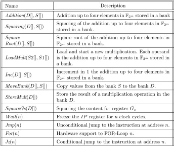
The complete instruction set is shown in table 1 whereS indicates the name of the source bank where the input operands are stored. Inside brackets indicate which registers of bankSare read, for example: F[0] indicates the register 0 of the bankF, andG[0,2,3] indicates the registers 0, 2, 3 of bankG. D indicates the destination bank where the result is stored. Inside brackets indicate which registers of bankD are written. Notice that more than one register of bankD
can be written at the same time with the same result.
Table 1: Instruction set for the proposed architecture.
Name Description
Addition(D[], S[]) Addition up to four elements inF2m stored in a bank
Squaring(D[], S[]) Squaring of the addition up to four elements inF2m stored in a bank.
Square Root(D[], S[])
Square root of the addition up to four elements in
F2m stored in a bank.
LoadMult(S2[], S1[])
Load and start a new multiplication. Each operand is the addition up to four elements inF2m stored in
a bank.
Inc(D[], S[]) Increment in 1 the addition up to four elements in
F2m stored in a bank.
MoveBank(D[], S[]) Copy values from the bankS to the bankD.
StoreMult(D[]) Store the result of a multiplication operation in the bankD.
SquareGs(D[]) Squaring the content for registerGs
Wait(n) Freeze theIP register fornclock cycles.
Jmp(n) Unconditional jump to the instruction at addressn.
For(n) Hardware support to FOR-Loopn.
Jz(n) Conditional jump to the instruction at addressn.
specific registers with in the bank, notice that more than one register within the bank can be read at the same time. The same format is used for the control instructionsJmp, For,Wait and Jz. For these instructionsOP2 and OP1 act like a 12-bit constant. This coding allows a total of four banks used as source banks and other four banks used as destination banks. If needed, more banks could be addressed by incrementing the number of bits in the fieldsOP1 and
OP2.
4.3
F
2marithmetic modules
4.3.1 Addition
In polynomial basis, an element A in the field F2m can be represented as a
(m−1)-degree polynomial as follows:
A=αm−1xm−1+αm−2xm−2+· · ·+α1x+α0=
m−1
X
i=0
αixi (9)
where A is normally represented as a m-bit vector containing all coefficients defining its corresponding polynomial, that is, A= (αm−1, αm−2,· · ·, α1, α0). Due to the polynomial representation, addition in F2m is computed using a
single bit-wise XOR operation. Notice that there is no carry propagation in field addition.
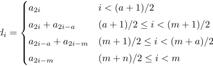
4.3.2 Square root
Square root is also a cheap operation when using trinomials as irreducible poly-nomial. Following the algorithm described in section 2.2.1, matrixM−1 can be computed off-line because the irreducible polynomial is the same when comput-ing the paircomput-ing. The matrix multiplicationM−1Ais very sparse, so just a couple of additions are needed. For the irreducible trinomialf(x) =xm+xa+ 1, the equation 10 performs the computation of D =Pd
ixim −1
i=0 , such that D2 =A modf(x) [30].
di=
a2i i <(a+ 1)/2
a2i+a2i−a (a+ 1)/2≤i <(m+ 1)/2
a2i−a+a2i−m (m+ 1)/2≤i <(m+a)/2
a2i−m (m+n)/2≤i < m
(10)
For the square root module, hardware cost is deduced from equation 10, it can be verified that an addition if required for (a+ 1)/2≥i <(m+a)/2. This results in a total of (m−1)/2 additions, namely XOR gates.
4.3.3 Squaring
As it is shown in equation 5, squaring consists in an expansion of the input vector interleaving a ‘0’ between each bit, followed by a modular reduction. PLFSR are used for this purpose. Figure 2 illustrate the design. For the squaring module, the cost in area is indeed only the cost of the modular reduction.
3 2 1 0 S1 S0R3R2R1R0S1 S0R3R2R1R0
CMD OP2 OP1
0 15
m bits
2m-1 bits
0
...
am-1 am-2 am-3 a0
0 0 0
MOD_RED(PLFSR) m bits
a1 0 a2
Figure 2: Squaring operation overF2m.
4.3.4 Modular reduction
Modular reduction is required within both multiplication and squaring modules. Representing f(x) as a bit-vector notice that fm = f0 = 1. Thus, xA(x) becomes a shift to the left operation onA(x) leading to a (m+ 1)-bit vector,
xA(x) = (am−1, am−2,· · ·. , a1, a0,0). The resulting bit vector is the same with an extra 0 at the least significant position. Ifam−1= 0, a reduction is not necessary. However, ifam−1= 1, the resulting polynomial is reduced modf(x), following equation 11, which definesxA(x) modf(x) consideringfm=f0= 1, where⊕represents a bitwise XOR operation and represents a bitwise AND operation. This expression is well modeled by the Linear Feedback Shift Register (LFSR) shown in figure 3. The combinatorial logic, CL-LFSR performs the required arithmetic to computexA(x) modf(x). Therefore,dCL-LFSR blocks could be connected in a cascade fashion to implement a parallel LFSR (PLFSR) and to obtainxdA(x) modf(x) in just one iteration. More details on the LFSR and the PLFSR are described in [41].
xA(x) modf(x) = (11)
(am−2⊕[fm−1am−1],am−3⊕[fm−2am−1], ..., a0⊕[f1am−1], am−1)
For computing a modular reduction using PLFSR, consider a polynomial
g(x) of degree 2m−1, The polynomialg(x) can be written asg(x) =g2(x)xm+
g1(x). The polynomialg1(x) does not require modular reduction, butg2(x)xm does. The complete modular reductiond is computed following the equation
g(x) modf(x) =g2(x)xm modf(x)+g1(x). The PLFSR cost ismXOR gates as stated above but only computes the first part of the modular reduction; additionally,mXOR gates are necessary to complete the operation. A total of 2mXOR gates are required for computing a modular reduction using PLFSR.
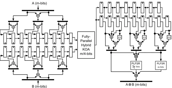
4.3.5 Multiplication
. . .
x·A(x) mod f(x) Combinatorial logic for LFSR
(CL-LFSR)
A(x)=am-1xm-1+am-2xm-2+...+a1x+a0 m
am-1
am-2 am-3 am-4 a0
fm-1 fm-2 fm-3 f1
xdA(x)mod f(x)
(CL-LFSR)1
m
A(x) m m...m m
(CL-LFSR)2 (CL-LFSR)d
m
Figure 3: Modular Reduction using Linear Feedback Shifts Registers.
A (m-bits)
B (m-bits)
Fully-Parallel
Hybrid KOA m/4-bits
<< << <<
A B (m-bits)
PLFSR -bits
m 2
PLFSR
m-bits
Figure 4: Serial-parallel multiplier based on Karatsuba-Ofman algorithm with modular reduction by Parallel Linear Feedback Registers.
bits. Finally, the 9 partial results are merged according to KOA to complete the multiplication. Figure 4 shows the architecture for theF2m multiplication
used in this work. This multiplier requires 9 clock cycles for computing a field multiplication. The output of the serial multiplier was designed to be registered, so after the field multiplication is computed, the result remains available at the module’s output.
odd indexes and even indexes instead of splitting in the most significant part and less significant part, saving one level of logic in each recursive call consuming the same hardware. Additionally, Zhou et. al. shown in [44] that for small inputs size the schoolbook algorithm present better results in resources and time than KOA. Based on that report, the recursive KOA calls were truncated after srecursions and then the schoolbook algorithm was used for the smaller multipliers. In this case, the truncation was implemented in the fully-parallel KOA ofm/4 bits.
Different to the serial multiplier proposed in [3], the integrates the modular reduction computation inside the field multiplier as is explained in [42]. The resource consumption and time processing of the multiplier module is improved. The theoretical cost of the serial multiplier is divided into three parts: the cost of the fully-parallel KOA (fp-KOA) module, the cost before the fp-KOA module, and the cost after the fp-KOA module, see figure 4. To simplify this analysis, only the special case ofmbeing an even number is considered, that is dm/2e=m/2 .
Each input of the serial multiplier is first split using the KOA-LFSR strategy; at this level inputs size ismbits andm/2 XOR gates are required by each input, so first level needsm XOR gates. In the second split the overlap-free strategy is used for three partial multiplications, at this level inputs size ism/2, som/4 XOR gates are required by each input of each partial multiplication, then second level needs 3m/2 XOR gates. Prior the fp-KOA module, the serial multiplier requires 5m/2 XOR gates.
The output of the fp-KOA module is of size m/2 bits, those outputs are merged to get 3 partial results of sizemusing the overlap-free technique. Each merge require 3 additions with operands pfm/2 bits, requiring 9m/2 XOR gates. The final merge has to be done using the KOA-LFSR technique. Two PLFSR are required, one formshifts and other form/2 with a cost of 3m/2 XORs gates for both PLFSR. Four more additions are required in the final merge, that is 4m
XOR gates are additionally require. The serial multiplier requires 10m XOR gates after fp-KOA module. No extra hardware is necessary for the modular reduction as this operation was integrated using PLFSRs.
Regarding the number of registers, each input requires nine register of size
m/4 to store the partial inputs. Partial results are momentarily stored in eight registers of sizem/2, the ninth partial result is taken directly form the output of the fp-KOA module. Nine more register of sizem/2 are used to store finally the partial results keeping the result available at any time. A total of 13mregisters are needed for the serial multiplier.
amount of XOR gates required forsrecursive calls of KOA.
S= (4n−3)
| {z }
1st level
+ 34n 2 −3
| {z }
2nd level
+ 94n 4 −3
| {z }
3th level
+· · ·+ 3s−14 n 2s−1 −3
| {z }
s-th level
= s
X
i=1
3i−14 n 2i−1 −3
(12)
Aftersrecursive calls, the KOA algorithm is truncated and the schoolbook algorithm is used. The schoolbook algorithm cost is quadratic, that isw2AND gates and (w−1)2 XOR gates are required, where w is the input size of the schoolbook algorithm [44]. Aftersrecursive calls of KOA,w=n/2(s+1). Then, considering that the actual input of the fph-KOA module is sizem/4, the hard-ware cost of the fp-KOA module is then expressed by equation 13.
S=
" s
X
i=1
3i−1 m 2i−1 −3
+ 3m 4 −1
2 #
·XOR+3m 2
8 ·AN D (13)
For the entire serial multiplier, the total amount of resources required is given in table 2. Cost is divided in the number of XOR gates, AND gates and registers.
Table 2: Theoretical cost of the serial KOA multiplier.
XORs ANDs REGs
Area
Ps
i=13i−1
m
2i−1 −3
+
3 m
4 −1
2
+23m
2
(3m2)/8 13m
4.4
Cryptoprocessor datapath
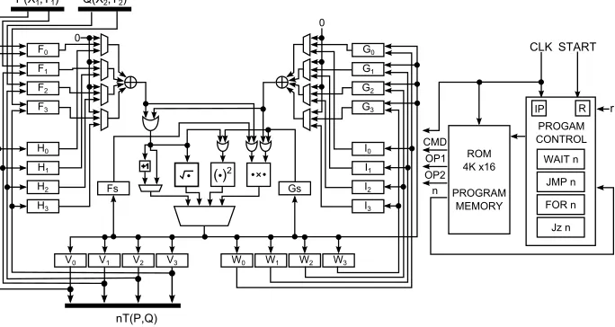
Figure 5 shows the proposed datapath. It contains six bank registersF, G,H,
I,V,W. Only banksF,G,H andIcan be used as source banks for arithmetic operations. For the multiplication, one operand comes from bankF or H and the other comes from bankG or I. Only banks V, W and Gcan be used as destination banks for arithmetic operations. TheMoveBankinstruction is used to copy the values from one bank to another but just certain movements are supported: from V to F or H, and from W to G or I. There are two extra registers,FsandGs, used as alternative inputs for multiplication. Additionally, the registerGs is connected to the squaring module.
G0 G1 G2 G3 F0 F1 F2 F3
V0 V1 V2 V3 W0 W1 W2 W3 Gs ( )2
nT(P,Q)
+ Fs
Q(X2,Y2)
P(X1,Y1)
H0 H1 H2 H3 I0 I1 I2 I3 ROM 4K x16 PROGRAM MEMORY PROGAM CONTROL CLK START FOR n WAIT n JMP n IP n OP2 CMD OP1 Jz n R r +1 0 0
Figure 5: Proposed architecture for computing bilinear pairings over binary fields.
and G also have two inputs, which means that there is a multiplexer at the input for selecting which of the two inputs will be written. Some OR gates are used to drive the right input to the arithmetic module. All arithmetic modules compute their respective operation at the same time, a 4-input multiplexer is used for selecting the right result. The extra hardware for computingA⊕1 is placed in the path of the addition.
Different to the datapath presented in [3], in this new version the bank H
and I are configured to be source banks for arithmetic operations. With this modification, the datapath reaches more flexibility in their operation.
4.4.1 Program control
Program control module is used to implement the instructionsJmp,For,Wait and Jz. These instructions make use of a 12-bit constant contained in the instruction itself. Inside this module there is the 12-bit Instruction Pointer register (IP) used to indicate the next instruction to be executed. A total of 4K instructions can be addressed. The “START” signal resets theIP register to ‘0’. Normally theIP register increments its value every clock cycle. When a control instructions is loaded, the next value of theIP register depends on the instruction.
4.5
Theoretical cost analysis
The theoretical cost in hardware of the complete cryptoprocessor is the addi-tion of each arithmetical module cost, plus the extra hardware required for the interconnection. In the following cost analysis, only is considered the usage of trinomial as irreducible polynomial for definingF2m.
The addition at the output of banksFandGis performed by a 4-input XOR, which in fact can be computed by three XOR gates of 2-inputs. Each addition is of sizem bits. In total 6mXOR gates are required for those additions. As depicted in figure 5, four OR gates of m bits are used to drive correctly the data. 4mOR gates are required in the cryptoprocessor datapath.
Without counting the cost of arithmetic modules, the most hardware usage relays on a series of multiplexers. One multiplexer of 4 inputs is used to select the output of the arithmetic modules. A single multiplexer of 4-inputs can be implemented with three multiplexers of 2 inputs. Prior the additions, there are eight multiplexers of 3 inputs, each one implemented with two multiplexers of 2 inputs. At the input of banksF andGthere are eight multiplexers of 2 bits per bank. Each multiplexer is of sizembits. The multiplexer for selecting. In total there are 27m multiplexers of 2 bits. The amount of registers is very straight forward. There 6 banks of 4 registers each, plus 2 extra registers (F sand Gs), each one ofmbits. 26mregisters are required in the cryptoprocessor datapath. The hardware support for control instructions is performed using 12-bits comparators, 12-bits multiplexers and 12-bits registers. The hardware cost and time delay of this module is very small compared with the cost of the arithmetic modules and the rest of the architecture. For these reasons the cost analysis has been depreciated as do not represent a significant cost.
In table 3, it is summarized the total cost of the proposed cryptoprocessor. Notice that most of the area computed theoretically is due to the multiplication module. The other modules with more area consumption are the multiplex-ers used in the datapath. Also notice that despite the datapath uses several registers, the serial multiplication consumes a third part of the total registers.
4.6
Programmability
The instructions set along with the datapath allow a lot of flexibility for pairing computing because of its programmability. Consider the algorithm depicted in figure 1 and assume that registersF0 to F3 contain the values x1, y1, x2, y2 as shown in figure 5. The additionG0 =F0+F2 is computed by the instruction Addition(G[0], F[0,2]), whileW2=G0+G1+G2+G3is computed by the instruc-tionAddition(W[0], F[0,2,3,4]). Notice that when only one register is accessed at the source bank and destination bank, the instruction Addition(D[], S[]) is equivalent to just move one register to other.
Table 3: Theoretical cost of the proposed cryptoprocessor.
Module XORs ANDs ORs MUXs REGs
Addition 6m - - -
-Multiplication
Ps
i=13
i−1 m
2i−1 −3
+ 3 m4 −12
+232m (3m
2)/8 - - 13m
Squaring 2m - - -
-Square Root (m−1)/2 - - -
-Datapath - - 4m 27m 26m
Total
Ps
i=13
i−1 m
2i−1 −3
+ 3 m4 −12
+ (40m−1)
2
(3m2)/8 4m 27m 39m
Now consider the multiplication s·(x1+x2+γ) in line 5 of algorithm 1. Both operands depend onγand previous multiplication is required to compute
x1= √
x1.
1)Inc(G[0], F[0]): computes=x1+ 1 and store it inG0 2)Addition(Fs, G[0]): movestoFs
3)SquareRoot(G[0], F[0]): computeG0= √
x1 4)Inc(G[0], G[0]): computeG0=
√
x1+ 1 5)Addition(G[1], F[2]): movex2to G1
6)LoadMult(F s, G[0,1]): begins·(√x1+x2+ 1)
whenγ= 0, consider the next sequence instead:
1)SquareRoot(G[0], F[0]): computeG0= √
x1 2)Addition(G[1], F[2]): movex2 toG1 3)LoadMult(F[0], G[0,1]): begins·(√x1+x2)
Notice here that the program complexity is closely related with the amount of operations and the data dependency. Also notice that other operations can be computed while the multiplication is being executed. For this example in line 5 of algorithm 1,y1+y2+ (1 +γ)·x1+δcan be computed in parallel with the multiplications·(√x1+x2+γ).
is required for computing this algorithm in the proposed architecture.
Arithmetic in the extended field is easily supported by the proposed crypto-processor independently of the tower field. Consider raising an element to the
q-th power. Equation 8 computes this operation for the tower field presented in [23]. Nevertheless, in [28] a different tower field is used, so raising an element to theq-th power is computed by equation 14. Both equations, 8 and 14 consist in computing four coefficients overF2m. Implementing this operation with the
proposed architecture consists in four instructionsAdditions(D[], S[]), the only consideration is that all coefficients of the elementGbe in the same bank.
Gq = (g0+g2) + (g2)x+ (g1+g3)x2+g3x4 (14)
5
Experimental results
5.1
Validation estrategy
The proposed architecture was implemented using VHDL as a description lan-guage. For design validation of arithmetical modules, C/C++ routines based on the library Miracl1 were used to generate 1000 random test data vectors for each module. A test bench was written to read the test vector from a file, to instantiate a particular module and to simulate its behavior for all the test vector generated. Xilinx ISim 13.2 was used as simulation environment. For all experiments, the underlying finite field was F21223 defined by the trinomial f(x) =x1223+x255+ 1, in order to reach a security level of 128-bits [27].
The full cryptoprocessor was validated using a similar strategy. Two versions of theηT pairing were used for testing the correct functionality of the datap-ath. First version named Barreto-Beuchat uses the Miller’s algorithm presented in [23] and the final exponentiation introduced in [26]. Second version named Ronan uses the version of theηT algorithm introduced in [28]. Finally, in order to validate the cryptoprocessor under some Pairing-based Cryptography appli-cation, the Identity-based Key Encapsulation Mechanism (ID-KEM) introduced in [45] was implemented in software using the C/C++ Miracl library. ID-KEM scheme consists in four algorithms which in conjunction have the purpose to es-tablish a shared key among two parties, starting from the receiver’s public key. In this case, the receiver’s public key is an identifier related to the receiver’s identity. ID-KEM requires the computation of two bilinear pairings, one extra pairing can be computed in order to ensures that the receiver’s private key is well generated. A total of 35 different identifiers were tested, resulting in a total of 105 bilinear pairing computations. This validation was performed for the two versions of theηT pairing algorithm presented previously.
1Copyright 2012 CertiVox IOM Ltd. Online available:
5.2
Implementation results
The design was implemented in FPGA devices, targeting both Xilinx Virtex-6 (xc6vlx130t) and Xilinx Virtex-4 (xc4vlx200) devices. FPGAs was chosen with comparative purposes, the design is not specific for FPGA devices. Even the Virtex-4 is old device, it was chosen for comparative purposes.
Program memory was implemented with Xilinx’s Block Memory Generator LogiCORE. Xilinx ISE 13.2 was used as synthesis tool using flags by default except for flags -iobuf FALSE and -register balancing YES. The -iobuf states if the synthesis tool attempts to match the inputs and outputs of the design with real pins on the target devices. The flag-register balancing moves regis-ters through combinatorial logic to evenly distribute the paths delay between registers, increasing the maximum clock frequency.
5.2.1 Serial multiplier
As mentioned in section 4.3, for implementing the fully-parallel hybrid KOA module inside the serial multiplier module, the KOA algorithm was truncated after s recursive calls. In [44] it was shown experimentally that the optimal value ofs depends on the implementation technology. In this sense, the serial multiplier was synthesized using several values ofs.
Table 4: Implementation results for serial multiplier using different values ofs.
s LUTs FFs Minimum period Latency A·T
1 40,969 18,244 2.817 ns 25.353 ns 1.04 2 34,734 17,306 2.647 ns 23.823 ns 0.83 3 31,262 17,344 2.882 ns 25.938 ns 0.81 4 28,518 17,507 3.144 ns 28.296 ns 0.80 5 28,990 15,904 7.902 ns 35.559 ns 1.03 6 31,720 15,904 9.325 ns 83.925 ns 2.66
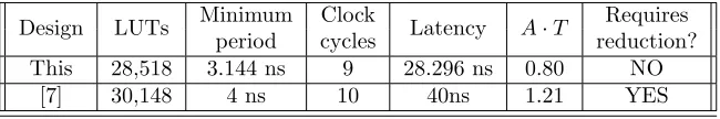
Since the proposed design is based on the serial multiplier reported by Ghosh et. al. in [7], a results comparison against that work is performed. In table 5 the best implementation achieved for the serial multiplier is compared against [7]. Notice that the proposed serial multiplier includes the modular reduction inside the multiplier, different to the multiplier reported in [7] which additionally requires a modular reduction module.
Table 5: Comparative ofF2m serial multipliers.
Design LUTs Minimum Clock Latency A·T Requires
period cycles reduction?
This 28,518 3.144 ns 9 28.296 ns 0.80 NO
5.2.2 Cryptoprocessor
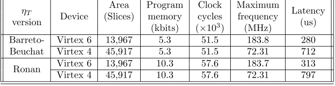
Table 6 shows the implementation results of the synthesis process. The required area is 13,967 slices for a Virtex 6 device. From this area, about 51.04% is used by the field multiplier; being this, as expected, the biggest individual module from all arithmetic modules. Nevertheless, the multiplexers inside each bank register consume a great amount of resources, a total of 35.02%. The remaining 13.94% of the area is used for the rest of the arithmetic modules and the program control unit. Notice how the area is closely related with the technology, for a Virtex 4 a total of 45,917 slices were used. This is due to one Virtex 6 slice contains 4 Look-Up Table (LUT) of 6 bits input, in contrast one Virtex 4 slice contains only 2 LUTs of 4 bits inputs.
The maximum clock frequency depends on the longest path delay among two registers, for the proposed architecture this path is inside the multiplier with 11 levels of logic. The maximum frequency that the architecture can operate with is 183.8 MHz for a Virtex 6. In the same way, time is closely related with the technology, Virtex 6 is a 40 nm device able to work with a clock frequency up to 1,600 MHz, while Virtex 4 is 90nm technology able to work with a clock frequency up to 72.31 MHz.
Results reported in this work outperforms the results previously reported in [3]. With the improvements done, the amount of hardware resources in about 15% in the case of a Virtex 6. While for a Virtex 4, resource consumption is reduced in about 10%. The reason of this reduction relies mainly in the new organization of the working registers, which allows the synthesis tool to find a more compact implementation. Maximum frequency in any case remains almost the same.
The amount of memory required by experiment Ronan is almost the double than the required by Barreto-Beuchat, this is because the operations in Ronan in general are more dependents so more instructions MoveBank(D[], S[]) were required. Additionally, the final exponentiation in Ronan requires a total of five multiplications over Fqk, while final exponentiation in Barreto-Beuchat only
performs one multiplication overFqk, so less code was needed.
Table 6: Implementation results of the proposed architecture for two different version ofηT algorithm.
ηT
Device
Area Program Clock Maximum
Latency version (Slices) memory cycles frequency (us)
(kbits) (×103) (MHz)
Barreto- Virtex 6 13,967 5.3 51.5 183.8 280
Beuchat Virtex 4 45,917 5.3 51.5 72.31 712
Ronan Virtex 6 13,967 10.3 57.6 183.7 313
Virtex 4 45,917 10.3 57.6 72.31 797
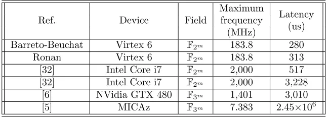
flexible implementations that uses general purposes microprocessors. This com-parative includes the fastest implementation of pairing algorithms in GPUs, and a specialized software library for pairing computations. This comparison only considers the processing time. In all cases the proposed cryptoprocessor com-putes the pairing algorithm faster. Although general purposes microprocessors or GPUs are very powerful technologies, they are limited to their own general purpose instruction set and fixed size operands. In this way, the proposed cryp-toprocessor may be used as a specialized co-processor for pairing computations, leaving the rest computations of any Pairing-based protocol to be executed by the general purpose microprocessor.
Table 7: Comparative of the proposed architecture with software implementa-tions.
Ref. Device Field
Maximum
Latency frequency
(us) (MHz)
Barreto-Beuchat Virtex 6 F2m 183.8 280
Ronan Virtex 6 F2m 183.8 313
[32] Intel Core i7 F2m 2,000 517
[32] Intel Core i7 F2m 2,000 3,228
[6] NVidia GTX 480 F3m 1,401 3,010
[5] MICAz F3m 7.383 2.45×10⁶
A comparison against state-of-art custom implementations of theηT pairing for binary fields is presented in table 8. All works reported in this table reach a security level of 128 bits except for [9], which achieve a security level of 105 bits. For this comparison, only the implementation results of the Barreto-Beuchat version of theηT pairing is considered. It is noticed that custom implementa-tions are faster than the proposed architecture, which is expected because cus-tom implementations make use of parallelization and other techniques in order to achieve faster results. A comparison with [9] make this statement more evi-dent, but the cost of faster architectures is the use of more hardware resources, which is also evident in this comparison. It can be observed that the area con-sumed by the proposed cryptoprocessor is very similar to works [7] and [8]. The
A·T product reached in this work is 3.91, which is just 1.35x bigger than [7] and 2.3x bigger than [8]. Compared to [9] theA·T product is 2.77x bigger, but notice that [9] only reaches a security level of 105 bits. These results show that custom architectures are slightly faster/smaller than the proposed design, but with all the flexibility achieved with the proposed architecture it is a fair cost.
Table 8: Comparative of the proposed architecture against custom architectures for binary fields.
Ref. Device Area
Maximum Clock
Latency A·T (Slices) frequency cycles (us) (Slices
(MHz) (×103) ×Seg.)
Barreto- Virtex 6 13,967 183.8 51.5 280 3.91
Beuchat Virtex 4 45,917 72.31 51.5 712 32.69
[7] Virtex 6 15,167 250 47.6 190 2.88
[8] Virtex 6 16,403 267 27.3 102 1.7
[9]* Virtex 4 78,874 130 2.4 18.8 1.41
*That work targeted a security level of 105 bits.
computation time, that work only achieve a security level of 66 bits whereas the proposed architecture achieves a security level of 128 bits. Comparing area consumption and processing time with the work reported in [35], the proposed cryptoprocessor outperforms that work in both parameters. Comparison with the ASIP reported in [40] is harder because the target devices of this thesis is a FPGA, not an ASIC; anyway it can be notice that the proposed architecture is able to execute a pairing algorithm 20x faster.
Table 9: Comparative of the proposed architecture against works in the litera-ture with some degree of flexibility.
Ref. Field Area
Maximum Clock
Latency A·T (Slices) frequency cycles (us) (Slices
(MHz) (×103) ×Seg.)
Barreto-F2m 45,917 72.31 51.5 712 32.69
Beuchat
Ronan F2m 45,917 72.31 57.6 797 36.59
[38]* F3m 1,851 203 27.8 137 0.25
[35] Fp 52,000 50 1,729 34,600 1,799
[40]** Fp 97kGates 338 N/R 15,800 N/A
*That work targeted a security level of 66 bits.
**That work targeted an ASIC using a 30 nm standard cell library.
6
Conclusion and future work
This work discussed the design and evaluation of a flexible cryptoprocessor able to manage several parameters for computing bilinear pairings, as the elliptic curve, the tower field, the distortion map, or the version of the pairing algo-rithm. These parammeters do not interferer with the security of cryptographic applications but affect the performance.
The design follows a modular approach so it can be constructed to support bilinear pairings defined on other fields asF3m. The results show that the
pro-posed design requires a similar amount of resources compared to related works. In addition, the processing time is shorter than other flexible architectures, in-clusive the proposed architecture is faster that software implementations. Also, the proposed architecture is very competitive in area and processing time against custom architectures of the state-of-art. In conclusion, the proposed design pre-serves the flexibility of the software while conpre-serves the acceleration in pairing computations of custom architectures. The compact instruction format allows smaller programs than related works, therefore using less program memory.
A thorough optimization process can be done to improve the maximum clock frequency, being the pipelining technique a first approach. As this pairing cryp-toprocessor was originally conceived within a whole system, the control unit can be replaced by a general soft-processor like a PicoBlaze and a communica-tion interface to send/receive the operands will be implemented in a HW/SW codesing; for this last purpose an initial idea is to use a shared memory approach so that a master processor uses this memory to transmit data and also to load the desired program.
References
[1] G. Frey and H.-G. Ruck, “A Remark Concerning m-Divisibility and the Discrete Logarithm in the Divisor Class Group of Curves,”Mathematics of Computation, vol. 62, no. 206, p. 865, Apr. 1994.
[2] A. Menezes, T. Okamoto, and S. A. Vanstone, “Reducing elliptic curve log-arithms to loglog-arithms in a finite field,”IEEE Transactions on Information Theory, vol. 39, no. 5, pp. 1639–1646, 1993.
[3] E. Cuevas-Farf´an, M. Morales-Sandoval, R. Cumplido, C. Feregrino-Uribe, and I. Algredo-Badillo, “A programmable FPGA-based cryptoprocessor for bilinear pairings overF2m.” inReconfigurable and Communication-Centric
Systems-on-Chip (ReCoSoC), 2013 8th International Workshop on. Darm-stadt, Germany: IEEE, 2013.
[5] X. Xiong, D. S. Wong, and X. Deng, “TinyPairing: A Fast and Lightweight Pairing-Based Cryptographic Library for Wireless Sensor Networks,” in 2010 IEEE Wireless Communication and Networking Conference. IEEE, Apr. 2010, pp. 1–6.
[6] Y. Katoh, Y.-j. Huang, C.-m. Cheng, and T. Takagi, “Efficient Implementation of the ηT Pairing on GPU,” Cryptology ePrint Archive: Report 2011/540, no. 540, 2011. [Online]. Available: http: //eprint.iacr.org/2011/540
[7] S. Ghosh, D. Roychowdhury, and A. Das, “High Speed Cryptoprocessor for
ηT Pairing on 128-bit Secure Supersingular Elliptic Curves over Charac-teristic Two Fields,” in Cryptographic Hardware and Embedded Systems -CHES 2011, 2011, pp. 442–458.
[8] J. Adikari, M. A. Hasan, and C. Negre, “Towards Faster and Greener Cryp-toprocessor for Eta Pairing on Supersingular Elliptic Curve overF21223,” in
19th International Conference, Selected Areas in Cryptography 2012, 2012, pp. 166–183.
[9] J.-L. Beuchat, J. Detrey, N. Estibals, E. Okamoto, and F. Rodr´ıguez-Henr´ıquez, “Fast Architectures for theηT Pairing over Small-Characteristic Supersingular Elliptic Curves,”IEEE Transactions on Computers, vol. 60, no. 2, pp. 266–281, Feb. 2011.
[10] J. H. Silverman, The Arithmetics of Elliptic Curves, 2nd ed. Springer, 2009.
[11] A. Joux, “A One Round Protocol for Tripartite Diffie Hellman,” Algorith-mic Number Theory, vol. 1838, pp. 385–393, 2000.
[12] W. Diffie and M. Hellman, “New directions in cryptography,”IEEE Trans-actions on Information Theory, vol. 22, no. 6, pp. 644–654, Nov. 1976.
[13] R. Dutta, R. Barua, and P. Sarkar, “Pairing-Based Cryptographic Protocols: A Survey,” Cryptology ePrint Archive: Report 2004/064, no. 64, 2004. [Online]. Available: http://eprint.iacr.org/2004/064
[14] R. Barua, R. Dutta, and P. Sarkar, “Extending Jouxs Protocol to Multi Party Key Agreement,” in Progress in Cryptology - INDOCRYPT 2003, 2003, pp. 205–217.
[15] D. Boneh and M. Franklin, “Identity-Based Encryption from the Weil Pair-ing,” in Advances in Cryptology - CRYPTO 2001, vol. 2139, 2001, pp. 213–229.
[17] F. Zhang and K. Kim, “ID-Based Blind Signature and Ring Signature from Pairings,” inAdvances in Cryptology - ASIACRYPT 2002. Springer Berlin / Heidelberg, 2002, pp. 533–547.
[18] A. Boldyreva, “Threshold Signatures, Multisignatures and Blind Signatures Based on the Gap-Diffie-Hellman-Group Signature Scheme,” inPublic Key Cryptography - PKC 2003, 2003, pp. 31–46.
[19] R. Sakai and M. Kasahara, “ID based Cryptosystems with Pairing on Elliptic Curve,” Cryptology ePrint Archive: Report 2003/054, no. 54, 2003. [Online]. Available: http://eprint.iacr.org/2003/054
[20] X. Cheng, J. Liu, and X. Wang, “Identity-Based Aggregate and Verifiably Encrypted Signatures from Bilinear Pairing,” in Computational Science and Its Applications - ICCSA 2005. Springer Berlin / Heidelberg, 2005, pp. 1046–1054.
[21] P. S. L. M. Barreto, H. Kim, B. Lynn, and M. Scott, “Efficient Algorithms for Pairing-Based Cryptosystems,” inAdvances in Cryptology - CRYPTO 2002, vol. 2442, 2002, pp. 354–369.
[22] V. S. Miller, “The Weil Pairing, and Its Efficient Calculation,”Journal of Cryptology, vol. 17, no. 4, pp. 235–261, Aug. 2004.
[23] P. S. L. M. Barreto, S. D. Galbraith, C. O. H´eigeartaigh, and M. Scott, “Ef-ficient pairing computation on supersingular Abelian varieties,” Designs, Codes and Cryptography, vol. 42, no. 3, pp. 239–271, Feb. 2007.
[24] S. D. Galbraith and J. F. Mckee, “Pairings on Elliptic Curves over Finite Commutative Rings,” Cryptography and Coding, vol. 3796, pp. 392–409, 2005.
[25] F. Hess, N. P. Smart, and F. Vercauteren, “The Eta Pairing Revisited,” IEEE Transactions on Information Theory, vol. 52, no. 10, pp. 4595–4602, Oct. 2006.
[26] J.-L. Beuchat, N. Brisebarre, J. Detrey, E. Okamoto, and F. Rodr´ıguez-Henr´ıquez, “A Comparison Between Hardware Accelerators for the Mod-ified Tate Pairing over F2m and F3m,” in PairingBased Cryptography
-Pairing 2008, 2008, pp. 297–315.
[27] D. Hankerson, A. Menezes, and M. Scott, “Software Implementation of Pairings,” in Identity-Based Cryptography, M. Joye and G. Neven, Eds. IOS Press, 2008, ch. XI, pp. 188 – 206.
[29] I. N. Herstain,Abstract Algebra, 3rd ed. Wiley, 1996.
[30] F. Rodr´ıguez-Henr´ıquez, A. D´ıaz-P´erez, N. A. Saqib, and C. K. Koc, Cryp-tographic Algorithms on Reconfigurable Hardware, ser. Signals and Com-munication Technology. Boston, MA: Springer US, 2006.
[31] J.-P. Escofier,Galois Theory, ser. Graduate Texts in Mathematics. New York, NY: Springer New York, 2001, vol. 204.
[32] D. F. Aranha, E. Knapp, A. Menezes, and F. Rodr´ıguez-Henr´ıquez, “Paral-lelizing the Weil and Tate Pairings,” in13th IMA International Conference, IMACC 2011, 2011, pp. 275–295.
[33] R. C. C. Cheung, S. Duquesne, J. Fan, N. Guillermin, I. Verbauwhede, and G. X. Yao, “FPGA Implementation of Pairings Using Residue Number System and Lazy Reduction,” in Cryptographic Hardware and Embedded Systems - CHES 2011, no. 07, 2011, pp. 421–441.
[34] N. Estibals, “Compact Hardware for Computing the Tate Pairing over 128-Bit-Security Supersingular Curves,” inPairing-Based Cryptography - Pair-ing 2010, vol. 6487, 2010, pp. 397–416.
[35] S. Ghosh, D. Mukhopadhyay, and D. Roychowdhury, “High Speed Flexible Pairing Cryptoprocessor on FPGA Platform,” in Pairing-Based Cryptog-raphy - Pairing 2010, vol. 6487, 2010, pp. 450–466.
[36] G. R. Blakely, “A Computer Algorithm for Calculating the Product AB Modulo M,” IEEE Transactions on Computers, vol. C-32, no. 5, pp. 497– 500, May 1983.
[37] M. Joye and S.-M. Yen, “The Montgomery Powering Ladder,” in Crypto-graphic Hardware and Embedded Systems - CHES 2002, ser. Lecture Notes in Computer Science, B. S. Kaliski, c. K. Ko¸c, and C. Paar, Eds., vol. 2523. Berlin, Heidelberg: Springer Berlin Heidelberg, Feb. 2003, pp. 291–302.
[38] J.-L. Beuchat, N. Brisebarre, J. Detrey, E. Okamoto, M. Shirase, and T. Takagi, “Algorithms and Arithmetic Operators for Computing the
ηT Pairing in Characteristic Three,” IEEE Transactions on Computers, vol. 57, no. 11, pp. 1454–1468, Nov. 2008.
[39] D. F. Aranha, J.-L. Beuchat, J. Detrey, and N. Estibals, “Optimal Eta Pairing on Supersingular Genus-2 Binary Hyperelliptic Curves,” inTopics in Cryptology CT-RSA 2012, ser. Lecture Notes in Computer Science, vol. 7178, 2012, pp. 98–115.
[41] M. Morales-Sandoval, C. Feregrino-Uribe, and P. Kitsos, “Bit-serial and digit-serial GF(2m) Montgomery multipliers using linear feedback shift reg-isters,”IET Computers & Digital Techniques, vol. 5, no. 2, pp. 86–94, 2010.
[42] E. Cuevas-Farf´an, M. Morales-Sandoval, A. Morales-Reyes, C. Feregrino-Uribe, I. Algredo-Badillo, P. Kitsos, and R. Cumplido, “Karatsuba-Ofman Multiplier with Integrated Modular Reduction for GF(2m),” Advances in Electrical and Computer Engineering, vol. 13, no. 2, pp. 3–10, 2013.
[43] H. Fan, J. Sun, M. Gu, and K. Lam, “Overlap-free KaratsubaOfman polynomial multiplication algorithms,” IET Information Security, vol. 4, no. 1, p. 8, 2010. [Online]. Available: http://digital-library.theiet.org/ content/journals/10.1049/iet-ifs.2009.0039
[44] G. Zhou, H. Michalik, and L. Hinsenkamp, “Complexity Analysis and Efficient Implementations of Bit Parallel Finite Field Multipliers Based on Karatsuba-Ofman Algorithm on FPGAs,” IEEE Transactions on Very Large Scale Integration (VLSI) Systems, vol. 18, no. 7, pp. 1057–1066, Jul. 2010.