A Single Phase High Power Factor AC-DC
converter with Soft Switching Characteristics
Neethu Venugopal1, Nimmy George2
PG Student [PE], Dept. of EEE, Sree Narayana Gurukulam College of Engineering, Kadayiruppu, Kerala, India1
Assistant Professor, Dept. of EEE, Sree Narayana Gurukulam College of Engineering, Kadayiruppu, Kerala, India2
ABSTRACT:This paper proposes an integrated high power factor ac-dc converter with soft switching characteristics. The circuit consists of a buck converter and a boost converter that integrates to form the proposed circuit topology. The boost converter operates in discontinuous-conduction mode (DCM) to perform the function of high power factor correction (PFC). The buck converter regulates the output voltage of the boost converter to supply stable dc voltage to the load. Both converters operate at high switching frequency. The active switches of the proposed converter operates at DCM for achieving zero-voltage switch-on(ZVS).The low-pass filter is used to remove the high frequency ripples of current. Circuit configuration and the circuit operation for eight modes explained. The simulink model of the proposed circuit provided.
KEYWORDS: Boost converter, Buck converter, Discontinuous-conduction mode (DCS), Zero-voltage switch-on, Power factor correction (PFC).
I.INTRODUCTION
Ac/dc converters have been widely used in many applications such as LED lighting systems, industrial drives, electric power distribution systems, telecommunication systems, energy conversion systems and other high power applications. The boost, buck-boost converters have been widely used as power factor correctors. The most popular topology in power factor correction application is the boost topology. A boost converter or step up converter is a power dc to dc converter with an output dc voltage which is greater than output dc voltage. The boost topology is simple, and it allows low distorted input currents and an almost unity power factor with different control techniques. At low line input, the switch conduction losses are high, because the input RMS current has the highest value and the highest step-up conversion is required. The inductor has to be over sized for large RMS currents at a low line input, and for the highest volt-seconds applied throughout the input-line range. As a result, a boost converter designed for universal-input PFC applications is heavily oversized, compared to a converter designed for a narrow range of input line voltages. Due to large energy storage filter capacitor at the output, the boost converter has inrush current problems that can be mitigated by using additional components. Here the boost converter performs the function of PFC to obtain high power factor and low current harmonics at the input line. The buck converter further regulates the dc-link voltage to provide a stable dc output voltage.
Hard switching operation of active switches causes many problems in the circuit. This generates high switching losses and introduces high voltage and current stresses on circuit components. The circuit efficiency and stability decreases. In the proposed circuit both active switches are turned on at ZVS. It assures high circuit efficiency and stability. PI control method is used in the proposed circuit.
II.CIRCUIT MODEL
The circuit topology is derived by integrating a boost converter and buck converter. The proposed circuit consists of a low-pass filter circuit, a diode-bridge rectifier, a boost converter, a buck converter. The buck converter is composed of Lb, D5, DS2,
S1
and C0. The boost converter is composed of Lp, DS1, S2 and Cdc. Both converters operate at aremove the high frequency current of the inductor current. The input line current becomes sinusoidal and in phase with the input line voltage. So that high power factor can be achieved. The buck converter regulates the output voltage of boost converter to supply stable dc voltage to the load. In order to prevent both the active switches conducting at same time, there is a short non-overlap time defined as “dead time”.
Fig. 1 Proposed ac/dc converter circuit topology
The proposed circuit shown in figure 1 consists of a low-pass filter circuit, a diode-bridge rectifier, a boost converter, a buck converter.
III.CIRCUIT OPERATION
The circuit operation of the proposed circuit can be described in eight operation modes.
a) Mode 1
Prior to mode 1, S1 is at “ON” state. Boost inductor current Ip is zero. The dc-link capacitor supplies the buck inductor
current Ib which flows through S1, D5, Lb, and C0. This mode starts when S1 is turned off by the gate voltage VGS1. At the
beginning of this mode, Ib is diverted from S1 to flow through the output capacitors CDS1 and CDS2. CDS1 charged and
CDS2 discharged. As the voltage across CDS2, that is VDS2 decreases to be lower than the rectified input voltage Vrec, then
the boost inductor current Ip starts to increase. WhenVDS2 equals to -0.7V, DS2 turns on and mode 1 ends.
b) Mode 2
At the beginning of mode 2, VDS2 maintained at about “-0.7V” by antiparallel diode DS2. After short dead time, S2 is
turned on by the gate voltage VGS2.The on resistance of S2 is small enough, most of Ib will flow through S2 from source
to drain. In this mode Ib is greater than Ip. Ib keep decreases and Ip increases from zero, since boost converter designed
to operate in DCM. Ib has two loops. A part of Ib flows through S2, rest are equal to Ip that flows through the line
voltage source, diode rectifier and Lp. This mode ends when Ip is greater than Ib.
c) Mode 3
In this mode Ip is greater than Ib. Ip has two loops. A part of Ip flows through S2 so the direction of current flow
naturally changes. Current flows from drain to source. The rest flows through buck converter, equals to Ib. In this mode
Ib keep decreases and Ip increases. This mode ends when Ib equals to zero, since buck converter designed to operate at
d) Mode 4
In this mode S2 remains on to carry Ip. Because of Ib is zero, the buck converter is at off state. Here Ip increases. The
output capacitor C0 supplies current to load. This mode ends when S2 is turned off by VGS2.
e) Mode 5
At the beginning of this mode Ib equals to zero. Current Ip reaches maximum when S2 turned off. Ip will be diverted
from S2 to flow through CDS1 and CDS2. CDS1 discharged and CDS2 charged. As the voltage across CDS1 decreases to be
lower than Vdc-V0 then Ib start to increase so that voltage across Lb becomes positive. When VDS1 equals to -0.7V, DS1
turns on and this mode ends. f) Mode 6
At the beginning of this mode, VDS1 maintained to about -0.7V by antiparallel diode DS1. After short dead time, S1 is
turned on by VGS1. On resistance of S1 is small enough, so that rest of Ip will flows through S1 in the direction from
source to drain. In this mode Ip is greater than Ib. There are two loops for Ip. A part of Ip flows through S1 to charge dc
link capacitor. The rest are equals to Ib, flows into buck converter. This mode ends when Ib is greater than Ip.
g) Mode 7
In this mode Ib is greater than Ip. Current Ip keep decreases and current Ib keep increases. Ib has two loops. A part of Ib
flows through S1, the direction naturally changed so that from drain to source. The rest flows through boost converter.
This mode ends when current Ip becomes zero.
h) Mode 8
In this mode S1 remains on and Ib keeps increasing. This mode ends at the time when VGS1 becomes a low level to turn
off S1. The circuit operation returns to mode1.
IV.SIMULATION
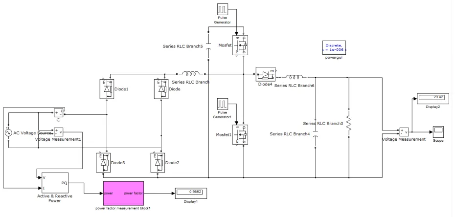
The simulink model of the proposed circuit for an open loop control is as shown in the figure 2. The output voltage waveform obtained is shown in the figure 3.
Fig. 2 Open loop control for proposed circuit
30V and it designed for 0.20 duty ratio. The open loop control of proposed circuit as shown in the figure 2 gives a PF of 0.9852
Fig. 3 Output voltage for open loop control circuit
The output voltage waveform obtained is shown in the figure 3. By using open loop control method the output obtained is 29.42V.
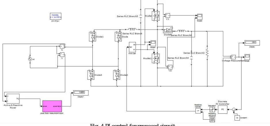
The simulink model of the proposed circuit for PI control is as shown in the figure 4. The output voltage waveform obtained is shown in the figure 5. The gate pulse waveform of switches is given in figure 6.
Fig. 4 PI control for proposed circuit
Fig. 5 Output for the PI control circuit
The output voltage obtained for the PI control method is as shown in the figure 5. PI control circuit gives an output voltage of 29.9V.
Fig. 6 Gate pulse generated for active switches
The gate pulses generated for the on/off operation of active switches is as shown in the figure 6. There is a short non-overlap time defined as “dead time”.
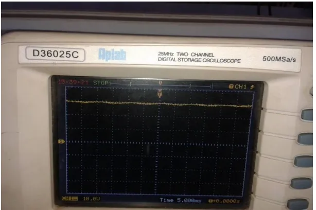
V.HARDWARE IMPLEMENTATION
Fig. 7 Proposed circuit hardware
The output waveform obtained is given in figure 8.
Fig. 8 Output waveform
Output voltage of the proposed circuit is 30V as per the design.
VI.RESULT
Proposed ac/dc converter is shown in the figure 1. By using open loop control circuit the ac/dc converter is as shown in figure 2, the power factor obtained is 0.9852. The circuit gives an output voltage of 29.42V. The output voltage waveform is given in figure 3. The proposed converter use PI control method as shown in figure 4. In the case of PI control the proposed circuit gives power factor of 0.9956 and the output voltage is 29.9V. The output voltage waveform is given in the figure 5. So PI closed loop control method is used in the ac/dc converter. The figure 6 shows gate pulses generated for the active switches that ensure dead time. The PI control assures high circuit efficiency and high power factor. The hardware implementation of the proposed circuit is given in figure 7. It provides an output voltage of 30V. The output voltage waveform is as shown in the figure8.
VII.CONCLUSION
through the intrinsic diodes of the MOSFETs. The boost converter performs the function of power factor correction. For the purpose boost converter is designed to operate at DCM. The buck converter in the circuit regulates the dc-link voltage to provide stable dc output voltage.. The proposed circuit is controlled by PI control method. It provides high power factor and assures circuit efficiency.
REFERENCES
[1] C. M. Wang, C. H. Lin, and T. C. Yang, “High-power-factor soft-switched dc power supply systems,” IEEE Trans. Power Electron., vol. 26, no. 2, pp. 647-654, Feb. 2011.
[2] J. M. Alonso, J. Vina, D. G. Vaquero, G. Martinez, and R. Osorio, “Analysis and design of the integrated double buck-boost converter as a high-power-factor driver for power-LED lamps ,” IEEE Trans. Ind. Electron., vol. 59, no. 4, pp. 1689-1697 April 2012,.
[3] R. T. Chen and Y. Y. Chen, ”Single stage push pull boost converter with integrated magnetic and input current shaping technique, ” IEEE Trans. Power Electron., vol. 21, no. 5, pp. 1193-1203, Sep. 2006.
[4] M. Z. Youssef, and P. K. Jain, “A novel single stage AC-DC self oscillating series-parallel resonant converter , ” IEEE Trans. Power Electron , vol. 21, no. 6, pp. 1735-1744, Nov. 2006.
[5] K. W. Seok, and B. H. Kwon, ”A novel single-stage half-bridge ac-dc converter with high power factor, ” IEEE Trans. Ind. Electron., vol. 48, no. 6, pp. 1219-1225, Dec. 2001.
[6] S. S. Lee, S. W. Choi, and G. W. Moon, “High-efficiency active-clamp forward converter with transient current build-up (TCP) ZVS technique, ” IEEE Trans. Ind. Electron., vol. 54, no. 1, pp. 310-318, Feb. 2007.
[7] D. L. O’Sullivan, M. G. Egan, and M. J. Willers, “A family of single stage resonant ac/dc converters with PFC, ”IEEE Trans. Power Electron., vol. 24, no.2, pp. 398-408, Feb. 2009.
[8] J. W. Yang and H. L. Do, ”High-efficiency ZVS AC-DC LED driver using a self-Driven synchronous rectifier,” IEEE Trans. Circuits and Systems –I: Regular Papers, vol. 61, no. 8, pp. 2505-2512, Aug. 2014.