Practical Implementation and Analysis of EMI Effects on Transistor as an Amplifier
circuit in CE & CB configurations
Mandeep Kaur Saini Ph.D Scholar, ECE Department Sant Baba Bhag Singh University
Padhiana,Jalandhar [email protected]
Dr. Anupamdeep Sharma Professor
Sant Baba Bhag Singh University Padhiana,Jalandhar [email protected]
Abstract: When electromagnetic interference takes place with the input pins of transistor working as an amplifier in Common emitter and Common Base Configurations, it can cause operation variation when practically implemented[9]. This paper deals with the investigation of EMI effects in amplifier circuit using different configurations[2][4]. This work presents evaluation of the EMI effects in transistor as an amplifier circuit by applying a range of EMI signals varying from 3KHz-30MHz with constant magnitude of 10V in series with input signal of 6Khz/10V. The EMI effects on the test circuit are predicted using ORCAD in terms of total job time, time step and output waveform. All the results compiled in the paper are simulated from the same. For easier understanding Bar graph is shown. The work presented shows the maximum range of EMI signals that a circuit can withstand and a range is also defined in which the circuit output is unaffected from EMI signal. Keywords: EMI, Transistor as an amplifier, Common Emitter and Common Base Configuration.
1. INTRODUCTION
The basic concept of electrical and electromagnetic interference involves an emanating source and an affected device or system. The transfer of energy between systems can occur through radiation, conduction, or induction. The actual transfer of energy is facilitated respectively through a transmission path, conductive path, or through magnetic coupling. The interference that affects wireless communication links is typically the result of radiated or conductive energy transfer. The condition of a conductive affect occurs when the signal is picked-up by a conductor attached to the affected system. Several studies related to EMI effects on electronic devices and circuits have been reported in the literature and EMI effects on Passive circuit elements such as resistor and the circuits containing these components have been investigated and analysed by experimental and simulation studies[5][6][7]. The results of these studies indicate that EMI may cause significant changes and incorrect operation of electronic circuits[3]. In this paper, we focused at EMI effects on basic circuit of transistor as an amplifier in CE and CB configurations.. The EMI effects are investigated with the utilization of simulator ORCAD, with interesting results.
Table 1: EMI SIGNAS USED AT DIFFERENT FREQUENCIES
Input signal EMI Signal Frequency range
EMI signal Amplitude
6KHz/10V 3KHz- 30Mhz 10V
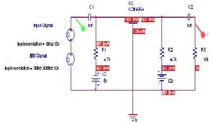
2. TEST CIRCIT
Transistor as an amplifier using CE configuration A common emitter amplifier is one of three basic single-stage bipolar-junction-transistor amplifier, which provides medium input and output impedance levels, typically used as a voltage amplifier. In this circuit the base terminal of the transistor serves as the input, the collector is the output, and the emitter is common to both (for example, it may be tied to ground reference or a power supply.)
In this paper, test circuit is presented on which the EMI effects will be analysed according to configuration shown in Table 1. The circuit of amplifier without EMI signal using CE configuration is shown in Fig. 1and the output waveform of this circuit is shown in Fig. 2.
[image:1.595.326.540.407.532.2]
Figure 1: CE amplifier without EMI signal and input signal 6Khz/10V
Figure 2: Transient Analysis of CE amplifier without EMI Signal
[image:1.595.316.543.570.672.2]Figure 3: CE amplifier with EMI signal from 3KHz-30MHz/10V and input signal 6Khz/10V
.
As shown in Fig 4, the output waveform is much affected when EMI signal is applied along with the input as compared to the output shown in Fig. 2 when there no EMI signal present.
Figure4: Transient Analysis of CE amplifier with EMI Signal
3. EXPERIMENTAL RESULTS
In Fig. 3 EMI signal is injected in series with input signal and applied between base and emitter of transistor. The simulation results are shown at different frequencies of EMI signal in Fig 5.
EMI EFFECTS WITH EMI SIGNAL AT FREQUENCY
30KHz- 30Mhz/10V
Inp ut Sign al
EMI Signa l
Tim e Step
Tota l Job Tim e (sec)
Pow er Diss ipati on
Simulation
6KH z/10 V
3kHz 16.2 3e-06
0.24 1.06 e-02w
6KH z/10 V
10KH z
6.49 6e-06 0.30
1.06 e-02w
6KH z/10 V
20KH z
6.16 0e-06 0.33
1.06 e-02w
6KH z/10
V 40KH
z 3.11 3e-06 0.38
1.06 e-02w
6KH z/10 V
80KH z
1.16 7e-06 0.30
1.06 e-02w
6KH z/10 V
100K Hz
824. 7e-09 0.34
1.06 e-02w
6KH z/10 V
500K Hz
105. 4e-09 1.31
1.06 e-02w
6KH z/10 V
1MHz 103.
0e-09 2.20
1.06 e-02w
6KH z/10 V
5MHz 18.9
7e-09
10.9 5
1.06 e-02w
6KH z/10 V
30M Hz
3.30 7e-09
69.0 9
1.06 e-02w
Figure 5: Output Waveform of CE configuration type transistor as an amplifier
A range of EMI signals varying from 3KHz-30MHz is applied keeping magnitude constant of 10V. As we can see from fig.4 that as the frequency varies from 3KHz to 30Mhz total job time and time step keep on changing but power dissipation is constant for all frequencies. At each frequency output waveform is predicted and if EMI signal Frequency is increased beyond 30Mhz the system is highly unstable.
4. TEST CIRCIT
Transistor as an amplifier using CB configuration A common base amplifier is one of three basic single-stage bipolar-junction-transistor amplifier, provides low input impedance and offering a high output impedance. In this circuit the emitter terminal of the transistor serves as the input, the collector is the output, and the base is common to both (for example, it may be tied to ground reference or a power supply.)
[image:2.595.39.261.56.181.2]in Table 1. The circuit of amplifier without EMI signal using CB configuration is shown in Fig. 6 and the output waveform of this circuit is shown in Fig. 7
[image:3.595.45.247.102.202.2].
[image:3.595.38.247.227.330.2]Figure 6: CB amplifier without EMI signal and input signal 6Khz/10V
Figure 7: Transient Analysis of CB amplifier without EMI Signal
Fig. 8 shows amplifier circuit with EMI signal in CB configuration and the output waveform of this circuit is shown in Fig. 9.
[image:3.595.40.256.414.538.2]Figure 8: CB amplifier with EMI signal from 3KHz-30MHz/10V and input signal 6Khz/10V
Figure 9: Transient Analysis of CB amplifier with EMI Signal
As shown in Fig 9, the output waveform is much affected when EMI signal is applied along with the input as compared to the output shown in Fig. 7 when there no EMI signal present
5. EXPERIMENTAL RESULTS
In Fig. 8 EMI signal is injected in series with input signal and applied between base and emitter of transistor. The simulation results are shown at different frequencies of EMI signal in Fig 10.
EMI EFFECTS WITH EMI SIGNAL AT FREQUENCY
3KHz- 30Mhz/100mV
Input Signal
EMI Signal
Time Step
Tot al Job Ti me (sec )
Pow er Diss ip-atio n
Simulation
6KHz/ 10V
3kHz 12.76
e-06
0.24 9.65 e-06w
6KHz/ 10V
10KHz 3.775
e-06
0.19 9.65 e-06w
6KHz/ 10V
20KHz 3.230
e-06
0.25 9.65 e-06w
6KHz/ 10V
40KHz 788.6
e-09
0.16 9.65 e-06w
6KHz/ 10V
80KHz 429.4
e-09
0.41 9.65 e-06w
6KHz/ 10V
100KH z
1.118 e-06
0.55 9.65 e-06w
6KHz/ 10V
60.10e -09
1.16 9.65
e -06w
60.1 0e-09
6KHz /10V
1MH z
107 .5e -09
2.00 9.65e -06w
6KHz /10V
5MH z
10. 39e -09
[image:3.595.38.258.575.693.2]6KHz /10V 30M Hz 2.4 27e -09 62.4 2 9.65e -06w
Figure 10: Output Waveform of CB configuration type transistor as an amplifier
A range of EMI signals varying from 3KHz-30MHz is applied keeping magnitude constant of 10V. As we can see from fig.9 that as the frequency varies from 3KHz to 30Mhz total job time and time step keep on changing but power dissipation is constant for all frequencies. At each frequency output waveform is predicted and if EMI signal Frequency is increased beyond 30Mhz the system has improved output response as shown in Fig. 10.
6. COMPARISION OF CE AND CB CONFIGURATION OF TRANSISTOR AS AN AMPLIFIER
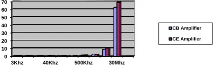
[image:4.595.34.281.54.83.2]Based on various factors like time step, Total Job Time and Power Dissipation, the common base and common emitter configurations are compared. The bar graphs of all factors is shown separately for both configurations to visualize the circuit which is more affected in the presence of EMI signal.
TABLE 2: COMPARISION OF CE AND CB AMPLIFIERS BASED ON VARIOUS FACTORS
Input Signal
EMI Signal
Amplifiers
CB Amplifier CE Amplifier
Time Step Total Job time Power Dissip ation Time Step Total Job time Power Dissipa tion 6KHz/
10V 3KHz
12.76 e-06
0.24 9.65e
-06w
16.23 e-06
0.24 1.06e
-02w
6KHz/
10V 10KHz
3.775 e-06 0.19
9.65e -06w
6.496 e-06 0.30
1.06e -02w
6KHz/
10V 20KHz
3.230 e-06 0.25
9.65e -06w
6.160 e-06 0.33
1.06e -02w
6KHz/
10V 40KHz
788.6 e-09 0.16
9.65e -06w
3.113 e-06 0.38
1.06e -02w
6KHz/
10V 80KHz
429.4 e-09 0.41
9.65e -06w
1.167 e-06 0.30
1.06e -02w 6KHz/ 10V 100KH z 1.118 e-06 0.55
9.65e -06w
824.7 e-09 0.34
1.06e -02w 6KHz/ 10V 500KH z 60.10 e-09 1.16
9.65e -06w
105.4 e-09 1.31
1.06e -02w
6KHz/
10V 1MHz
107.5 e-09 2.00
9.65e -06w
103.0 e-09 2.20
1.06e -02w
6KHz/
10V 5MHz
10.39 e-09 8.63
9.65e -06w
18.97
e-09 10.95
1.06e -02w
6KHz/
10V 30MHz
2.427 e-09 62.42
9.65e -06w
3.307 e-09 69.09
1.06e -02w
Fig11. Shows the bar chart of time step for both configurations and shows that time step of CE amplifier is higher than CB amplifier from 3KHz-80Khz and becomes equal above 100KHz.
[image:4.595.30.295.352.765.2]Figure11. Bar Chart Of Time step Of CE and CB configuration amplifiers
Fig.12 shows the total job time response of both CE and CB configurations which presents that total time taken by the circuit to simulate is more for CE configuration than CB configuration. Total Job Time of CE and CB amplifier is constant for the range 3KHz-100KHz and increased beyond 500KHz.
Figure12. Bar Chart Of Total Job Time Of CE and CB configuration amplifiers
Power dissipation graph is shown in Fig.13 which is constant of Both CE and CB configurations for the frequency range 3KHz-30MHz.
Figure13. Bar Chart Of Power Dissipation Of CE and CB configuration amplifiers
Power dissipation graph is shown in Fig.12 which is constant of Both CE and CB configurations for the frequency range 3KHz-30MHz.
CONCLUSION
In this paper the investigation of EMI effects on Transistor as amplifier circuit using two configurations like common base and common emitter is being analyzed and simulated. A detailed analysis is carried out for EMI signals used at different frequencies and Simulated results show that EMI can cause degradation of operation mostly at
80Khz-0.00E+00 5.00E-06 1.00E-05 1.50E-05 2.00E-05
3Khz 40Khz 500Khz 30Mhz
CB Amplifier CE Amplifier 0 10 20 30 40 50 60 70
3Khz 40Khz 500Khz 30Mhz
CB Amplifier CE Amplifier 0.00E+00 2.00E-03 4.00E-03 6.00E-03 8.00E-03 1.00E-02 1.20E-02
3Khz 40Khz 500Khz 30Mhz
[image:4.595.339.556.376.446.2]transistor an amplifier. But this degradation decreases beyond 10MHz-30Mhz for CB configuration only and output has less effect of EMI signal as shown in Fig 10. So from simulation results it is concluded that EMI can cause degradation of transistor circuit operation mostly when the frequency range raised beyond 80KHz/10V and has no effect of EMI on amplifier circuit below 10 V.
REFERENCES
[1] O.Galip Saracoglu, Recai Kihe, A Simulation Study on EMI Effects in Autonomous Chua’s Chaotic Circuit,IEEE, 2003
[2] Graffi, S., Masetti, G. and Golzio, D., New Macromodels and Measurements for the Analysis of EM1 Effects in 741 Op-amp Circuits, IEEE Trans. OnEMC, vol. 33, no 1, pp. 25-34, 1991.
[3] Florean, D., PineHi M. and Tomasin, P., Analysis of RFI Effects in Voltage Regulator ICs: Measurement Techniques, Picking Capability,
Prediction and Protection Methods, 2000 IEEE lnt. Symp. On EMC, Washington D.C., August 2000.
[4] Florean, D., Marchiori, F., Pinelli M. and Tomasin, P.,Analysis of EMI Effects in Op-Amp IC's: Measurement Techniques and numerical prediction, 2001 IEEE Int. Symp. On EMC, Montreal, August 200 1. [5] Richardson , R. E., Modeling of Low-Level Rectification RFI in Bipolar Circuiby, IEEE Trans. on EMC, vol. EMC-21, pp. 307-31 1, 1979. [6] F. Fiori, V. Pozzolo, “On the Effects of RF in Voltage Regulator Integrated Circuits”, InternationalSymposium on EMC, Zurich 1997. [7] F. Fiori, V. Pozzolo, “On the Effects of RF on Bipolar Integrated
Circuits”, International Symposiumon EMC, Rome 1996.
[8] D. Golzio, S. Graffi, G. Masetti, “New macromodelfor the analysis of EM1 effects in LF355 Op-Amp circuits”, International Symposium on EMC, 1989.
[9] J.Jiraprasertwong, C. Jettanasen,”Practical Design of a Passive EMI filter for Reduction of EMI Generation”, Proceedings of International Multiconference of Engineers and Computer Scientists,Vol II, Hongkong, 2015.