125
Abstract—In recent days, the main motto of VLSI designers is to reduce the power and area as devices are becoming battery-operated, compact and require enhanced functionality and features. Due to the scaling and shrinking of devices, the transistor leakage power has increased at an exponential rate. In this paper, analysis on the research based on the Modified gate diffusion input technique (m-GDI) which has gained much attention in recent days are encompassed. Consequently, 31 research papers homologous to m-GDI technique are assessed and analysed based on the numerous targets. In this review, we present the m-GDI Technique, a low power technique and scrutinize the modern breakthroughs with several pros and cons. The thorough examination is done on finding the inclusion of the issues, methodologies, simulation tools and technologies used.
IndexTerms— Area, Leakage Power, m-GDI, Scaling.
I. INTRODUCTION
LOW-POWER configuration has transformed into an essential matter in VLSI design, particularly for mobile gadgets and high-density frameworks. As the integration density on the chip increments, basic concerns with respect to the size and power dissemination of the components emerges. Also, it has been demonstrated that an increase in 100 C ascend in operating temperature of the electronic gadgets cause a 100% collapse rate. So, the number of transistors to be fabricated in an electronic device must be made as least as possible with an end goal to decrease the area and to squander less power [1].
As the feature size reduces, the following effects arises in the circuits – a) due to reduction in channel length, it results in increase of sub threshold leakage current, b) the output of circuits results in high transients, c) increase in gate leakage current. In order to reduces these losses various VLSI design techniques are implemented like Static CMOS logic,
Manuscript revised May 13, 2019 and published on June 5, 2019
Gautam Nayan, Bachelor of Engineering, Dept. of ECE, Sri Siddhartha Institute of Technology, Tumakuru, India
Rajesh Kumar Prasad, Bachelor of Engineering, Dept. of ECE, Sri Siddhartha Institute of Technology, Tumakuru, India
Praveen Kumar Y G, Assistant Professor, Dept. of ECE, Sri Siddhartha Institute of Technology, Tumakuru, India
Dr. M Z Kurian, Prof. & Head, Dept. of ECE, Sri Siddhartha Institute of Technology, Tumakuru, Indie
Pass transistor logic (PTL), Gate Diffusion Input (GDI) logic and Modified Gate Diffusion Input (m-GDI) logic.
Static CMOS Logic: In this logic, the output is strongly driven between VDD and VSS. This is due to the fact that the
output is coupled to VSS via an N-block and to VDD via a
P-block. With the input to the circuit being fixed, it devours just the leakage current from the couple of transistors. During switching operation, the circuit draws an extra current which is required for charging and discharging the internal capacitances and the load [2,3].
Pass Transistor Logic: It characterizes a few logic families, that lessens the transistor count needed to realize the logic gates by taking out excess transistors. The logic uses primary inputs to drive source, gate and drain terminals. In conventional CMOS logic, primary inputs are permitted to operate exclusively on gate terminals [2-4].
Pass-transistor logic styles are primarily been subdivided into two types: a) CPL- uses NMOS based pass-transistor circuits. b) DPL-uses both NMOS and PMOS pass-transistors.
Complementary Pass-Transistor logic (CPL): As the threshold voltage drop of NMOS transistor degenerates the ―high‖ level of pass-transistor output nodes, the full swing output is achieved using CMOS inverters. CPL circuits are generally connected to the arithmetic building blocks which results in high-speed operation because of its low input capacitance and diminished transistor count [2,4].
Double Pass-Transistor Logic (DPL): In order to achieve reduced noise margins in CPL, twin PMOS transistor branches are attached to N-tree in DPL. This outcomes in enlarged input capacitances. Still, its symmetrical arrangement and twofold-transmission attributes for the slow speed of operation emerging from expanded loading. The full swing operation enhances circuit execution at decreased supply voltage with restricted threshold voltage scaling [2,4]. The principle standpoint of PTL implementation over standard CMOS implementation are - a) PTL based circuits offers small node capacitances which in turn provides high speed operation. b) Since, the quantity of transistors used to actualize the circuit is reduced, it offers less power dissipation. However, PTL implementations generally faces the problem of significant static power dissipation, as logic high levels at the input of regenerative inverters is not the full scale VDD. Hence, the PMOS device in the inverter is not fully
turned off, which results in direct path static power dispersal [2].
Gate Diffusion Input Technique (GDI): - This method permits decrease in power dispersal, delay and area
A Review On Modified Gate Diffusion Input Logic: An
Approach For Area And Power Efficient Digital System
Design
126 consumed by the digital circuits, while keeping up lower
multifaceted nature of logic design. GDI cell comprises of 3 inputs – Gate input of PMOS and NMOS(G), input to drain/source of PMOS (P) and input to drain/source of NMOS (N). The bulk of both PMOS and NMOS are coupled to their diffusion P and N respectively in order to reduce bulk effect. The GDI technique accounts for reduction of both sub threshold leakage current and gate leakage current in contrast to traditional CMOS design [5-7].
Modified Gate Diffusion Input Technique (m-GDI): - It is a new technique for digital system design that results for low power consumption. The design using m-GDI technique accounts for high speed operation, reduced power dissipation, lesser transistors count and minimal area consumption circuits. m-GDI technique is adopted from the GDI technique. m-GDI cell also comprises of 3 input terminals – Gate input of PMOS and NMOS(G), input to drain/source of PMOS (P) and input to drain/source of NMOS (N) with bulk of PMOS constantly coupled to VDD and bulk of NMOS to VSS [8-11].
The output of digital circuits implemented using GDI technique suffers threshold voltage drops. m-GDI excels the drawback of GDI cell. With the scaling in technology, the impact of source body voltage on the transistor threshold potential gets surpassing shortened [8].
In this paper, the design implementation of digital circuits through m-GDI is surveyed. An exhaustive survey is orchestrated on modified gate diffusion input technique- the exploration challenges and the accomplishments are presented in this paper. Correspondingly, 31 research papers are viewed as identified with m-GDI and these papers are surveyed.
Concerning the exploration, the perusal is provided depending on the different criteria such as power dissipation, transistor count, delay, area and various limitations of different design techniques
II. TAXONOMY OF VLSI DESIGN
In perspective of the outline drove in excess of 31 research papers, the taxonomy of different VLSI design techniques for implementation of digital circuits is introduced in this segment. The way towards gathering 31 research papers from the writing is talked about underneath. At first, we choose four well known standard digital libraries, such as IEEE explore, Elsevier, IJSR, ICEE to
gather the articles
(http://ieeexplore.ieee.org/Xplore/home.jsp),
(https://www.elsevier.com/catalog) and so on, afresh, Google scholar is likewise used to discover the articles which are issued in other than these four standard digital libraries (https://scholar.google.co.in/).
In all the standard digital libraries, we explored the terms like, ―Gate diffusion input technique‖ and ―Modified Gate diffusion input technique‖ to gather every one of the articles published till now. At that point, we separated the gathered articles by finding the most pertinent articles which are distributed precisely under this theme. At last, we got 31 articles for the basic audit of modified gate diffusion input technique.
The scientific classification of the review is made by considering the methodology used to diminish the losses in the digital circuits. The individual methodologies in each research paper are portrayed here. The fame of the electronic circuits in different building frameworks raised the requirements for the scientific categorization of plan method of digital circuits.
A. TRADITIONAL APPROACH
In this approach, the accompanying classification, such as static CMOS logic and pass transistor logic (PTL) are scrutinized along with the advantages and drawback of each technique.
A.I. Static CMOS Logic
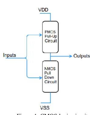
CMOS is referred to complementary-symmetry metal–oxide–semiconductor. It uses both NMOS and PMOS to construct logic gates. A static CMOS circuit is composed of two networks:
Pull-up Network – A set of PMOS transistors connected between VDD and output line. It is referred as pull up
network as output is pulled to VDD when PMOS is on
[2,4].
Pull-down Network – A set of NMOS transistors connected between Vss and output line. It is referred as
[image:2.595.358.507.436.626.2]pull-down network as output is pulled to Vss potential when NMOS is on [2,4].
Figure 1: CMOS logic circuit
A general CMOS logic circuit is shown in the Figure 1. For an N-input logic gate, CMOS circuit uses 2N number of transistor (N- NMOS and N-PMOS). When one MOSFET is ON, other will be in OFF state and hence the name complementary. In addition, in order to implement Ex-OR gates, multiplexers and flipflops efficiently often pass gates or transmission gates are utilized [2].
127 scaling and transistor sizing and so offers dependable
operation at minimal voltages and random (even nominal) transistor sizes (ratio less logic) [2,3].
The downside of CMOS circuit is, 2N nos. of transistors in the circuit increases, it outcomes in increased input loads, thus results in increased power dissipation, area and temperature during operation. Still, better execution of the gate can be accomplished with a PMOS/NMOS width ratio of just about 1.5, and this ratio additionally diminishes in profound deep submicron technologies, where the carrier drift velocities in NMOS and PMOS transistors nearly wind up equivalent to velocity saturation. Another snag of the CMOS circuits is, due to series arrangement of transistors in the output phase the circuit suffers weak output driving capability[2].
A.II. Pass Transistor Logic
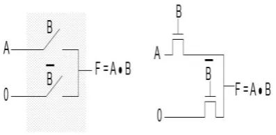
[image:3.595.66.265.409.506.2]In pass transistor logic, the source side of the logic network is associated with a portion of the input signals rather than the power lines. The main standpoint is that, one pass-transistor network (either NMOS or PMOS) is adequate to implement the logic function, which outcomes in reduced count of transistors and lesser input loads, primilarly when NMOS devices are employed. Thus, area, power consumption and temperature also reduced during device operation [2,3]
Figure 2: AND gate using Pass Transistor logic Figure 2 shows AND gate implementation using pass transistor logic. Since, the NMOS transistors can only pass a voltage in the range (0, VDD-VTH ) swing restoration is
necessary while passing a logic ―1‖ to prevent static currents at the outputs of following inverters or logic gates [2,3]. Figure 3 shows an approach to reduce threshold voltage drop.
Figure 3: A method to reduce the threshold voltage drop by using (a) NMOS & PMOS in parallel; (b) swing reclamation inverters.
So as to disjoin gate inputs and outputs and to dispense tolerable output driving capabilities, inverters are for the most part are fixed to the gate output. As, the MOS networks are associated with varying gate inputs as opposed to consistent power lines, only a solitary path through each network must be dynamic immediately so as to prevent shorts between inputs. Consequently, each pass-transistor network must perceive a MUX structure, which restrains the count of logic functions that could be actualized effectively [2,8].
The layout of pass-transistor cells are much complex and less effective because of sporadic transistor positioning and high wiring necessities. Pass-transistor logic circuits with swing reclamation circuitry are delicate to scaling in voltage and transistor sizing as for circuit robustness (decreased noise margins). Hence, dependable performance of logic gates isn‘t ensured at low supply voltages or smaller transistor sizes. The circuit results in large short -circuit because of contending signals in the swing reclamation circuitry [2,3].
Distinctive kinds of pass transistor logic styles are: (a) Complementary Pass-Transistor Logic (CPL): A
CPL gate comprises of two NMOS logic networks (one for each signal rail), a pair of small pull-up PMOS transistors to overcome the swing degradation, and a pair of inverters at the output for the reciprocal output signals [2]. The upside of CPL over PTL are low input loads, proficient XOR and MUX realizations and better output driving capabilities. However, the disadvantage of CPL are significant number of hubs or nodes and high wiring requirements because of dual rail signals and wasteful acknowledgement of basic gates [2,4]. (b) Double Pass-Transistor Logic (DPL): Here, both
PMOS and NMOS logic networks are utilized in parallel. This offers full swing at the output (i.e., no signal reclamation logic is required), and stability of the circuit is thusly high. Still, the transistor count is particularly large and increased count of nodes prompts to significant capacitive loads [2].
Table 1 and Table 2 shows qualitative logic style comparison of traditional logic styles between different logic style [2] and power delay product of basic gates respectively
Table 1 and Table 2 shows qualitative logic style comparison of traditional logic styles between different logic style [2] and power delay product of basic gates respectively.
Table 1: Qualitative Logic Style Comparison [2]
Logi c style
[2] #rai
ls [2]
I/O Decou ple [2]
#MOS Netwo rks [2]
Swin g Rest
ore [2]
Outp ut drivi
ng [2]
Robust ness
[2]
CM OS
Sin gle
Yes n + p No medi um –
[image:3.595.60.284.633.768.2]128 Good
CPL Dua l
Yes 2n Yes Good Medium
DPL Dua l
Yes 2n+2p No Good High Table 2: PDP (fJ) Of Simple Logic Cells [3]
@Vdd=3.0v, T= 60 0
PDP (fJ)
AND 4
XOR NAND
2
2:1 MUX
4:1 MUX CMOS
[3]
57.7 56.0 26.1 57.8 49.8
CPL [3]
34.0 25.7 25.7 47.4 34.9 Figure 4 shows variation of power delay product for different channel lengths for 2:1 multiplex and 2 input NAND gate implemented using CMOS and PTL logic [4]. An exhaustive correlation between the PTL and Static CMOS logic style is introduced [2]
Figure 4: PDP of (a) CMOS type 2-input multiplexer, (b) PTL type 2-input multiplexer, (c) normalization of (b) by (a), (d) CMOS type 2-input NAND, (e) PTL type 2-input NAND, (f) normalization of (e) by (d) [3]
B.MODERN APPROACH
Traditional CMOS design technique has been a choice for most of the digital system designs. The real preferred standpoint of CMOS circuits over Pass transistors circuits i.e. single polarity MOS circuits (either NMOS or PMOS based), is that these circuit offer very minimal leakage and the static power dispersal is negligible. Nonetheless, the
power dispersal of CMOS circuits are dependent on the recurrence of operation. If the input signal frequency increases, the power dispersal of the CMOS circuits increases. The main limitation of CMOS circuits compared to Pass transistors and dynamic circuits is slow speed of operation [5].
In this segment, we will discuss about another technique for low power digital system design. These techniques allow lessening of power utilization, area and the delay of digital circuits, while keeping up low design multifaceted nature. The performance of these circuits are contrasted and the tradition CMOS and various PTL design as for the count of transistors used to actualize the circuits, layout area, delay and power dissipation.
B.I. Gate Diffusion Input Technique
Gate diffusion input technique (GDI) is a methodology for low power digital system design. It solves most of the drawbacks presented in traditional approach. A. Morgenshtein portrayed a new design GDI cell that permits the reduction in delay, area and power dissipation [4]. An extensive variety of complex logic functions can be actualized using only a transistor count of two. This technique is acceptable for designing high speed, power efficient circuits utilizing lesser transistor count (contrasted with traditional CMOS and PTL approach) [6,7].
[image:4.595.61.289.337.637.2]The implementation of all the logic functions are not achievable in standard p-well CMOS process, yet can be effectively implemented in twin-well CMOS or SOI technologies [5]. Figure 5 shows basic GDI cell.
Figure 5: Basic GDI cell
GDI diminishes both sub threshold leakage and gate leakage current when contrasted with conventional CMOS. GDI cell structure is distinctive from the existing PTL techniques, and has some critical highlights, which permits enhancements in design multifaceted nature level, no. of transistors, static power dissemination and logic level swing [5]. Table 3 shows the basic Boolean functions that can be actualized utilizing the two transistor GDI cell.
[image:4.595.373.488.442.594.2]129 The performance of GDI cell degenerates when utilized in
and underneath 90nm technology. When substrate is attached to any of the active region (source or drain), body effect is demolished in underneath equation [8,12].
VTH = VTH0 + γ (
ηVDS (1)
where ‗VTH‘ represents the threshold voltage, VSB
represents source body voltage, ‗VTH0‘ represents zero bias
threshold voltage, ‗γ‘ represents substrate bias coefficient, ‗ ‘ is fermi potential, ‗VSB‘ Source to substrate voltage,
‗VDS ‗drain to source voltage and ‗η‘ is drain induced barrier
lowering coefficient [8].
The digital circuits designed using GDI technique suffer threshold voltage VSB at their outputs homologous to
circuits utilizing Pass-Transistor Logic (PTL). Since, the allocation of VDD and VSS to PMOS and NMOS isn‘t
predetermined in case of GDI, issue of low voltage swing emerges and consequently, it is difficult for digital design implementation. These voltage drops devalue the execution of the circuit attributable to less current drive. In order to overcome the threshold voltage drops repetitive regenerative inverters are used which accounts for larger area occupancy of the digital circuit and disperses static power in direct path in series connected inverters as gate to source voltages of off transistors are amplified [8].
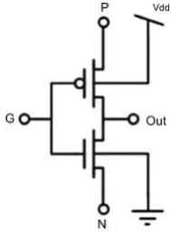
B. II. Modified Gate Diffusion Input Technique(m-GDI)
Modified gate diffusion input technique is a novel scheme for designing area and power efficient digital circuits with high speed operation. It is embraced from the GDI technique. m-GDI cell looks analogous to the basic GDI cell aside from the bulk of PMOS permanently attached to VDD and the bulk
[image:5.595.60.287.87.220.2]of NMOS to gnd [8]. A broad variety of logic functions can be actualized utilizing a solitary m-GDI cell. The basic m-GDI cell is depicted in the Figure 6.
Figure 6: Basic m-GDI cell
m-GDI cell vanquishes the drawback endured by basic GDI cell. As the technology scales down, the impact of source-body voltage on transistor threshold voltage gets exceptionally reduced i.e. the linearized body coefficient ' γ ' in equation (1) diminishes, making m-GDI relevant in 65 nm technology and below [1,8,12].
The implementation of digital circuits through m-GDI technique results in reduction of 60-90% of transistors required when contrasted with the traditional CMOS and PTL implementation. Thus, resulting in significant reduction of area and power consumption. The m-GDI cell looks similar to the GDI cell and hence can implement various function as shown in Table 4. Generally, the realization of basic logic functions using conventional CMOS technique requires a transistor count of 6-12, whereas they can be actualized utilizing a solitary m-GDI cell which comprises of a single PMOS and NMOS transistor shown in Figure 6. The comparison of transistors required for implementation of distinctive logic gates and functions are manifested in below Table 4 [8].
Table 4: Comparison of transistor count used to implement basic logic gates using m-GDI and Static CMOS logic style
[8]
FUNCTION CMOS m-GDI
AND 6 2
NAND 4 4
OR 6 2
NOR 4 4
A’B 6 2
A’+B 6 2
MUX 12 2
NOT 2 2
III. COMPARISON AND ANALYSIS
In this section, various circuits implemented using the m-GDI technique are shown and compared with the traditional CMOS, PTL and GDI based circuits. The comparative analysis is carried out regarding the transistor count required, delay, area, power and speed.
In paper [13,14,15], the design of full adder circuit utilizing m-GDI technique is proposed. In paper [13], 5 different designs of full adder architecture employing m-GDI technique has been implemented with a transistor count of 16T, 14T, 12T, 10T and 8T. The proposed designs are implemented in 250nm technology and simulation is carried out using Tanner EDA with BSIM3v3 with the supply voltage going from 1V to 5V in steps of 0.5V. The aspect ratio of both NMOS and PMOS transistor is taken as 2.5/0.25µm. The execution analysis of different m-GDI based full adder is carried out with reference to CMOS, PTL and GDI technique comsidering the transistor count required, power dispersal and delay offered.
[image:5.595.313.540.382.524.2] [image:5.595.120.215.661.792.2]130 scheme. Since, the GDI based logic gates experiences
threshold loss at their output, mixed threshold voltage transistors are employed to overcome the threshold loss using m-GDI technique. MVT scheme reduces leakage current and enhances the execution of the circuits. The proposed full adder requires a transistor count of 10T. The circuits are implemented in 45nm technology and simulated using BSIM4 Ver4.5.0 in HSPICE. The aspect ratio of PMOS and NMOS transistor is taken as 6/1 and 3/1 respectively.
In paper [15], the full adder circuit designed using m-GDI technique requires a transistor count of 10T. The circuit is implemented in 180nm technology using Cadence Virtuoso environment using bulk CMOS process. The proposed design is contrasted with respect to the tradition CMOS design technique which requires a transistor count of 30T. For the performance analysis of m-GDI based full adder circuit is carried out with respect to traditional design technique the transient analysis is carried out with a rise and fall time of 2ns.
In paper [16], the design of full adder circuit employing GDI approach is proposed. The adder circuit is implemented in 45nm technology in CADENCE environment. The proposed adder employs 10 transistors in GDI design approach and 30 transistors in the conventional CMOS approach.
From the Table 5, it can be found that, full adder design using m-GDI is utilizes lesser number of transistors, consumes lesser power and offers least delay when contrasted with traditional design conveyed in the paper [13,14,15,16]. Figure 7 depicts the comparison of number of transistors required for implementing the different full adder designs. Figure 8 depicts the power-delay performance of the distinct full adder designs.
[image:6.595.315.555.86.643.2]Table 5: Comparative Analysis of performance of Full Adder Circuit.
Figure 7: Comparison of number of transistors [13],[14],[15],[16]
Figure 8: Comparison of Power and Delay Performance [13],[14],[15],[16]
131 In paper [18], the proposed CSLA adder is
implemented in 90nm technology and simulated using TANNER EDA tool. The proposed design provides multi path for carry propagation and the carry select operation is done prior to the computation of final sum as compared to conventional design which offers single path for the carry propagation.
In paper [19,20], the design of carry select adder employing GDI technique has been proposed. The paper [19], proposes the design of 1-bit and 8-bit carry select adder. The GDI CSLA is contrasted with the traditional CMOS CSLA design. The design has been implemented in 90nm technology using Cadence Virtuoso Tool. The conventional CMOS CLSA design has also been implemented using D-latch.
In paper [20], the proposed 2-bit CSLA employs single stage scheme in which the partial sum is generated for the given inputs and later according to the input carry, the carry selection is performed followed by the generation of full sum. The proposed design is implemented in 90nm technology. The proposed design uses GDI XOR gate in half sum generation and full sum generation unit which reduces the transistor count as contrasted with the conventional CSLA, thus resulting in less power dissipation and delay.
In paper [21], a 4-bit parallel adder architecture is implemented employing m-GDI technique. The proposed design is implemented in 180nm technology and simulated using cadence virtuoso tool. The 4-bit parallel adder is actualized using 10T m-GDI full adder.
In paper [11,22,23,24,25,26], the design of various multipliers using m-GDI technique are discussed. In paper [11], the design of 4x4 array multiplier is proposed. The design is simulated in 180nm UMC technology utilizing Cadence Virtuoso Environment. The proposed design is a regular 4x4 bit array multiplier.The paper proposes a novel design of full swing AND gate, half adder and full adder. The design is based upon a hybrid topology which uses m-GDI based XOR and XNOR logic gates along with transmission gates and pass transistors.
In paper [22], the implementation of 4-bit, 8-bit and 16-bit Radix 4 Booth Multiplier is proposed. The simulation is carried out in 0.25µm technology using MICROWIND2 VLSI CAD tool. The aspect ratio of both nMOS and pMOS were taken to be 2.0/0.25μm. For the implementation of booth multiplier initially Booth encoder, 1-bit full adder and partial product generator are designed. The partial product generator uses Wallace tree to add all partial products. The final result of multiplication is obtained by addition of sum and carry using a carry select adder circuit.
In paper [23], a novel architecture of 16-Bit Multiplier is proposed. The proposed multiplier circuit is simulated on Mentor Graphics tool using AMI 0.5μm CMOS technology. The aspect ratio of both pMOS and nMOS transistors were taken to be 2.5/0.25μm. The 16-bit multiplier circuit was implemented by combining different modules i.e. 2‘s complement generator, partial product generator, Wallace Tree adder, booth encoder, and final adder. The design of partial product generator uses 2:1 multiplexer and the final adder uses a Wallace Tree adder.
In paper [24], the design of Hybrid 4-bit Radix-4 Booth Multiplier is proposed. The proposed design is
implemented using TANNER tool at 45nm technology. The multiplier is implemented using hybrid topologies which combines various modules such as Booth Encoder, Partial product multiplexer, full adder and add cell.
In paper [25], the design of 8-bit Vedic multiplier is proposed. The proposed multiplier is implemented on 180nm technology using Cadence Virtuoso Tool. The Vedic multiplier is designed utilizing Urdhva Tiryagbhyam sutra with 4 nos. of 4-bit Vedic multiplier and 3 different adder circuits with different number of transistors resulting in minimization of area and decrease in power dissipation.
[image:7.595.313.563.320.498.2]In paper [26], an optimized 4-bit array multiplier designed is proposed. The proposed circuit is implemented on 90nm technology and the simulation is carried out with the help of Mentor Graphics Pyxis schematic tool. The multiplier is implemented using AND gates which generate the partial product terms and these terms are added up utilizing 4 half adders and 8 full adders implemented using m-GDI technique.
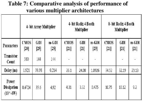
Table 7: Comparative analysis of performance of various multiplier architectures
Table 7 gives the comparative analysis of performance of various multiplier implemented using different design techniques. The multipliers implemented using m-GDI technique offered least transistor count and less power dissipation and delay.
132
Figure 9: Comparison of Power and Delay performance [20], [21], [23], [25]
In paper [27,28,29], various flip flops are implemented using m-GDI technique. In paper [27], synchronously clocked NOR-based JK flip-flop design is proposed. The design is implemented in 45nm technology using Tanner SPICE using BSIM ver 4.5.0. The aspect ratio of nMOS and pMOS transistors were taken to be 2/1 and 4/1 respectively. The JK flip flop is implemented using m-GDI based NOT, NAND and NOR gates. The design offers lesser delay, area and power utilization when contrasted with the JK flip flop designed using traditional design technique.
In paper [28], the design of master-slave D-flip flop utilizing Non-dominated Sorting Genetic Algorithm II (NSGA-II) is proposed. The design employs carbon nanotube field effect transistor (CNTFET). The proposed m-GDI cell is based upon the basic GDI cell which employs CNTFET transistors and dynamic threshold MOSFET technique. The circuit is implemented in 32nm technology and the NSGA-II algorithm is combined in MATLAB software and BSIM PTM in the H-SPICE software and the simulation results are obtained for Si-MOSFET and CNTFET based M/S D-FF.
In paper [29], the design of T-flip flop employing CNTFET transistors is proposed. The design is implemented in 32nm technology for CNTFETs and 48nm technology for Si-MOSFETs and the simulation is carried out with Stanford and BSIM PTM models with the help of H-SPICE software. The aspect ratio for P-CNTFET and N-CNTFET were taken to be equal to have minimum value whereas for the conventional design the ratio was taken 2 to 1 for pMOS and nMOS transistors. The m-GDI design employing CNTFET resulted in minimum area, power and delay in contrast to the conventional design employing Si-MOSFET.
[image:8.595.307.549.235.788.2]Table 8 gives the comparative analysis of performance of various flipflop circuits designed using different design techniques. From the comparative analysis it is found that the flip flops designed using m-GDI technique offers least delay, area and power dissipation. Figure 10 shows the transistors count required to implement different flip flop using various design techniques. Figure 11 shows comparison of power and delay performance of the different flip flop designs.
Table 8. Comparative analysis of performance of JK- FF, D-FF and T-FF
JK-Flipflop [27] M/S D-Flipflop [28] T-Flipflop [29] Si-MOS FET CN TF ET Si-MOSF ET CN TF ET Pa ra me ter C M O S G D I m-G DI m-C2 MO S [30] G D I [3 1] m-GD I Mo difi ed C M OS [32 ] GD I [33 ] m-GD I N u m be r of tr an sis to rs
32 1 6
16 24 1 8
14 24 22 16
De la y (n s) 20 0 1 0 0. 6 2 2. 42 0.05 36 0. 0 5 3 0.04 14 0.0 606 0.0 502 0.0 132 Po we r (µ W ) 0. 25 10 0. 4 5 0 1 0. 11 19
1.39 1. 5 1
0.33 42. 7
0.0 474
133
Figure 10: Comparison of number of Transistors [28], [29], [30]
Figure 11: Comparison of Power and Delay Performance [28], [29], [30]
IV. DISCUSSION
This segment introduces the research gap of existing design techniques with their future proposal
A.Research Gap and Issues
The recognizable proof of existing gap from the writing and tending to the issues introduced in the writing is vital. Here we deliver the issues related to different design techniques for digital circuits. The design of digital circuit using traditional technique requires large transistor count which results in greater power dissipation and delay. The design using CMOS technique requires 2N number of transistors to implement a Boolean expression involving N inputs, which increases the input loads and results in slow speed of operation. The PTL design technique results in high complexity due to irregular arrangement of transistors and these circuits are sensitive to transistor sizing and voltage scaling.
The design using modern technique requires a lesser transistor count and offers minimal delay and power dispersal. The GDI approach was proposed for fabrication in Silicon on Insulator (SOI) and twin-well CMOS process which offered the realization of wide variety of logic functions utilizing two transistors only. But the GDI based circuits suffer from the threshold loss at the output of digital circuits and hence offer lesser current drives.
The m-GDI technique overcomes the drawback the of GDI technique. As the technology reduces, the effect of source body voltage on the transistor threshold voltage gets truncated. From the literature survey it is found that the m-GDI based circuits often results in threshold loss when fabricated using traditional CMOS process. Thus, in order to
achieve full swing output, cascaded regenerative inverters are used at the output of the m-GDI cells which in turn increases the area of circuits.
B.Recommendation for Future Work
This segment proposes the feasible outcomes of future work and approach to broaden existing methodologies
The problem of the low swing output of digital circuits implemented using m-GDI technique can be overcome by utilizing the Full Swing GDI technique (FSGDI). The FSGDI utilizes a solitary swing restoration transistor to achieve full swing output from the digital circuits. The swing restoration transistor is activated only whenever there is threshold voltage drop i.e. VTH occurs at the output. The swing
restoration transistor has a diffusion input like the diffusion input of GDI but are of inverse type. FS-GDI cells are proficient alternatives to regenerative buffers.
The threshold loss observed at the output of conventional m-GDI technique can be overcome by using CNTFET technology. The CNTFET provides various advantages over the Si-MOSFETs. The width of N-CNTFET and P-CNTFET can be taken to be equal and hence it offers a design which consumes lesser area as compared to design using nMOS and pMOS. For the fabrication of CNTFET, a single wall carbon nano tube are used. By changing the chirality vector of the carbon nano tube, the threshold voltage of the CNTFET can be changed since the threshold voltage VTH is inversely
proportional of Carbon nano tube chirality vector
V. CONCLUSION
This paper dispenses the relative evaluation of execution of various digital circuits implemented using different design techniques. The main target of this investigation was to compare and analyse the performance of different digital circuits implemented using m-GDI techniques with respect to those designed using conventional techniques. Here, 31 research papers were taken from IEEE, ICEE, IRJET etc. Also, we have presented the taxonomy of different approaches for the low power VLSI design.
134
REFERENCES
[1] Divya Soni and Mihir V. Shah, Review on Modified Gate Diffusion Input Technique, IRJET 2017.
[2] Reto Zimmermann and Wolfgang Fichtner, Low-Power Logic Styles: CMOS Versus Pass-Transistor Logic, IEEE Journal of Solid-State Circuits, VOL. 32, NO.7, JULY 1997.
[3] Kyoung Hwa Lee, Scaling Characteristics of logic cells: Pass-Transistor logic Versus CMOS logic, SMDL Annual, 1999.
[4] Pankaj Verma, Ruchi Singh and Y. K. Mishra, Modified GDI Technique - A Power Efficient Method for Digital Circuit Design, International Journal of Advanced Technology in Engineering and Science Volume No.01, Issue No. 10, October 2013.
[5] Arkadiy Morgenshtein, Alexander Fish and Israel A. Wagner, Gate-Diffusion Input (GDI) - A Technique for Low Power Design of Digital Circuits: Analysis and Characterization, IEEE,2002. [6] Sudeshna Sarkar, Monika Jain, Arpita Saha and Amit Rathi, Gate
Diffusion Input- A design for fast digital circuit (implemented on 180nm technology), IOSR Journal of VLSI and Signal Processing (IOSR-JVSP), Volume – 4, Issue 2, March- April 2014.
[7] Simran kaur, Balwinder Singh and D.K Jain, Design and Performance Analysis of Various Adders and Multipliers Using GDI Technique, International Journal of VLSI design & Communication Systems (VLSICS) Vol.6, No.5, October 2015.
[8] Arkadiy Morgenshtein Idan Shwartz, Alexander Fish, Gate Diffusion Input (GDI) Logic in Standard CMOS Nanoscale Process, 2010, IEEE 26-th Convention of Electrical and Electronics Engineers in Israel.
[9] Uma.Ramadass and P. Dhavachelvan, New Low Power Delay Element in Self Resetting Logic with Modified Gated Diffusion Input Technique, IEEE-ICSE2012 Proc., 2012, Kuala Lumpur, Malaysia. [10] S.Swettha, S.Rashmi, Dr.N.S.S Reddy and Dr.R.Hemalatha, Area and
Power Efficient MAC unit, SPACES- 2018.
[11] Mahendra Kumar Lariya and D. K. Mishra, A Low Power Array Multiplier Design using Modified Gate Diffusion Input (GDI), Volume 4 Issue 8, International Journal of Science and Research (IJSR), August 2015.
[12] Krishnendu Dhar, Design of a High Speed, Low Power Synchronously Clocked NOR-based JK Flip-Flop using Modified GDI Technique in 45nm Technology, 2014, ICACCI.
[13] R.Uma and P. Dhavachelvan, Modified Gate Diffusion Input Technique: A New Technique for Enhancing Performance in Full Adder Circuits, 2nd International Conference on Communication, Computing & Security, 2012.[14] Krishnendu Dhar, Design of a Low Power, High Speed, Energy Efficient Full Adder Using Modified GDI
and MVT Scheme in 45nm
Technology, International Conference on Control, Instrumentation, Communication and Computational Technologies,2014.
[15] Khoirom Johnson Singh, Tripurari Sharan and Huirem Tarunkumar, High Speed and Low Power Basic Digital Logic Gates, Half- Adder and Full-Adder Using Modified Gate Diffusion Input Technology, STM Journals 2018.
[16] Pragati Sheel and Dr. Rajesh Mehra, Comparative Analysis of Gate Diffusion Input Based Full Adder, IOSR Journal of VLSI and Signal Processing (IOSR-JVSP) Volume 6, Issue 3, Ver. I, 2016. [17] Padmanabhan Balasubramanian and Johince John, Low Power Digital
design using modified GDI method, IEEE, 2006.
[18] S. R. Baliji, Dr. R. Manikandan, V. Vasudhevan, Scaling Down Area – Delay - Power Efficient of Carry Select Adder Using GDI, 2018, International Journal of Engineering Research & Technology (IJERT).
[19] Govind Prasad,V Shiva Prasad Nayak,S Sachin,K Lava Kumar and Soma Saikumar, Area and Power Efficient Carry- Select Adder, IEEE International Conference On Recent Trends In Electronics Information Communication Technology, May 20-21, 2016.
[20] Siva Rongali and Rajanbabu Mallabarapu, Gate Diffusion Input- Based Design For Carry Select Adder, 2018, Springer
[21] G. S. Smitha and H. V. Ravish Aradhya, mGDI based parallel adder for low power applications, 2017, Springer.
[22] Laxmi Kumre, Ajay Somkuwar and Ganga Agnihotri, Implementation of Radix 4 Booth Multiplier using MGDI technique,
International Conference on Microelectronics, Communication and Renewable Energy- 2013.
[23] M. Vinay Babu, M. Damodhar Rao and Dr. V.V.K.D.V. Prasad, A Novel Architecture of 16-Bit Multiplier Using Modified Gate Diffusion Input Logic, International Journal of Computer Science and Information Technology & Security (IJCSITS), Vol.6, No4, July- August 2016.
[24] Mr. Saurabh Katariya and Mr. Manish Singhal, A Hybrid 4-bit Radix-4 Low Power Booth Multiplier With High Performance, IEEE International Conference on Recent Advances and Innovation in Engineering (ICRAIE ), 2016.
[25] Shashank S Meti, Bharath C N, Praveen Kumar Y G and Kariyappa BS, Design and Implementation of 8-bit Vedic Multiplier using mGDI Technique, 6th IEEE International Conference on Advances in Computing, Communication and Informatics, pp:1923-1927,
2017.
[26] Pinninti Kishore, P. V. Sridevi and K. Babulu, Low Power and High Speed Optimized 4-bit Array Multiplier using MOD-GDI Technique, 2017 IEEE 7th International Advance Computing Conference.
[27] Krishnendu Dhar, Design of a High Speed, Low Power Synchronously Clocked NOR-based JK Flip-Flop using Modified GDI Technique in 45nm Technology, IEEE International Conference on Advances in Computing, Communication and Informatics (ICACCI), 2014.
[28] Ebrahim Abiri, Zobeideh Bezareh and Abdolreza Darabi, The Optimum Design of a Master-Slave D-Flip Flap (M/S-DFF) based on the modified GDI (m-GDI) Method Using Non-dominated Sorting Genetic Algorithm II (NSGA-II), 2016, 24th Iranian Conference on Electrical Engineering (ICEE).
[29] Ebrahim Abiri,Mohammad Reza Salehi and Abdolreza Darabi, Design and Simulation of Low- Power and High Speed T- Flip Flap with the Modified Gate Diffusion Input (GDI) Technique in Nano Process, The 22nd Iranian Conference on Electrical Engineering (ICEE 2014), May 20-22, 2014.
[30] J. M. Rabaey, Anantha Chandrakasan, Borivoje Nikolic, Digital Integrated Circuits: A Design Perspective, Second Edition, Prentice Hall, 2007.
[31] A. Morgenstein, A. Fish, I. Wagner, An Efficient Implementation of D Flip-Flop Using the GDI Technique, ISCAS ‘04, pp.673-676, May 2004.
[32] Ken Martin, Digital Integrated Circuit Design, Oxford university press, 2000.
[33] S. Ziabakhsh and M. Zoghi, Design of a Low-Power High-Speed T Flip-Flop Using the Gate-Diffusion Input Technique, Telecommunications forum TELFOR , pp.1470-1473, 2009
![Figure 4 shows variation of power delay product for different channel lengths for 2:1 multiplex and 2 input NAND gate implemented using CMOS and PTL logic [4]](https://thumb-us.123doks.com/thumbv2/123dok_us/749392.1085976/4.595.61.289.337.637/figure-variation-product-different-channel-lengths-multiplex-implemented.webp)
![Figure 7: Comparison of number of transistors [13],[14],[15],[16]](https://thumb-us.123doks.com/thumbv2/123dok_us/749392.1085976/6.595.315.555.86.643/figure-comparison-of-number-of-transistors.webp)
![Figure 9: Comparison of Power and Delay performance [20], [21], [23], [25]](https://thumb-us.123doks.com/thumbv2/123dok_us/749392.1085976/8.595.58.265.83.387/figure-comparison-power-delay-performance.webp)
![Figure 10: Comparison of number of Transistors [28], [29], [30]](https://thumb-us.123doks.com/thumbv2/123dok_us/749392.1085976/9.595.57.287.93.362/figure-comparison-of-number-of-transistors.webp)
