A Monthly Journal of Computer Science and Information Technology
ISSN 2320–088X
IJCSMC, Vol. 2, Issue. 4, April 2013, pg.604 – 609
RESEARCH ARTICLE
© 2013, IJCSMC All Rights Reserved
604
Implementation of Cryptographic
Algorithm on FPGA
Prof. S. Venkateswarlu1, Deepa G.M2, G. Sriteja3
1
Department of Computer Science, K L University, Vaddeswaram, Andhra Pradesh, India
2
Department of Computer Science, K L University, Vaddeswaram, Andhra Pradesh, India
3
Department of Computer Science, K L University, Vaddeswaram, Andhra Pradesh, India
Abstract— Advanced Encryption Standard (AES), a Federal Information Processing Standard (FIPS), is an approved cryptographic algorithm that is used to protect electronic data. The AES can be programmed in software or built with hardware. The paper presents a hardware implementation of the AES algorithm on FPGA. The algorithm was implemented in FPGA using Spartan 3E starter kit and Xilinx ISE development suite. The purpose of this attempt was to test the correctness of the implemented algorithm and to gain experience in optimization of algorithm structure for the embedded implementation in the target application.
Key Terms: - AES algorithm; hardware implementation; FPGA
I. INTRODUCTION
The importance of cryptography applied to security in electronic data transactions has gained essential relevance during the last few years. Everyday many users generate and interchange large amount of information in various fields through Internet, telephone conversations, and e-commerce transactions. These and other examples of applications deserve a security point of view, not only in the transport of such information but also in its storage. This can be achieved by various techniques such as password, cryptography and biometrics. In this sense, cryptography techniques are especially useful.
In cryptography, the AES, also known as Rijndael, is a block cipher adopted as an encryption standard by the US government, which specifies an encryption algorithm capable of protecting sensitive data [1, 2]. The AES algorithm is a symmetric block cipher that can encrypt and decrypt information. The AES algorithm uses cryptographic keys of 128, 192, and 256 bits to encrypt and decrypt data in blocks of 128 bits [3, 4]. The hardware implementation of this algorithm can provide either high performance or low cost for specific applications. At main communication channels or heavily loaded servers it is not possible to lose processing speed, which drops the efficiency of the overall system while running cryptography algorithms in software. On the other hand, a low cost and small design can be used in smart card applications, which allows a wide range of equipment to operate securely.
The AES algorithm can be efficiently implemented by hardware and software. Software implementations cost the smallest resources, but they offer a limited physical security and the slowest process. Besides, growing requirements for high speed, high volume secure communications combined with physical security, hardware implementation of cryptography takes place.
© 2013, IJCSMC All Rights Reserved
605
This paper deals with an FPGA implementation of an AES encryptor/decryptor using an iterative looping approach with block and key size of 128 bits. Organization of the rest of this paper is as follows. Section 2 provides a brief overview of AES algorithm.II. OVERVIEW OF AESALGORITHM
The AES algorithm is a symmetric block cipher that can encrypt and decrypt information. The algorithm is composed of three main parts: Cipher also known as encryption, Inverse Cipher also known as decryption and Key Expansion. Cipher converts data to an unintelligible form called ciphertext while Inverse Cipher converts data back into its original form called plaintext. Key Expansion generates a Key Schedule that is used in Cipher and Inverse Cipher procedure. Cipher and Inverse Cipher are composed of specific number of rounds illustrated in Table 1. For the AES algorithm, the number of rounds to be performed during the execution of the algorithm is dependent on the key length [5].
Table 1. AES
Block size (Nb) Key length (Nk) No. of rounds (Nr)
AES-128 4 4 10
AES-192 4 6 12
AES-256 4 8 14
For both its Cipher and Inverse Cipher, the AES algorithm uses a round function that is composed of four different byte-oriented transformations: SubBytes, ShiftRows, MixColumns and AddRoundKey.
Inputs and outputs: The input and output for the AES algorithm, each consists of sequences of 128 bits. The Cipher Key for the AES algorithm is a sequence of 128, 192 or 256 bits. The basic unit for processing in the AES algorithm is a byte, so the input bit sequence is first transformed into byte sequence. In the next steps a two-dimensional array of bytes (called the State) is built. The State array consists of four rows of bytes, each containing Nb bytes, where Nb is the block size divided by 32 (number of words). All internal operations of the
AES algorithm are then performed on the State array, after which its final value is copied to the output (State array is transformed back to the bit sequence).
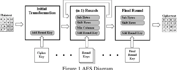
Cipher: Using round function, which is composed of four different byte-oriented transformations, the Cipher converts input data (the input data is first copied to the State array) to an unintelligible form called ciphertext. After an initial Round Key addition, the State array is transformed by implementing a round function with the final round differing slightly from the first Nr−1 rounds. The round function is parameterized using a key
schedule that consists of a one-dimensional array of four-byte words (Round Key) derived using the Key Expansion routine. All Nr rounds (in Table 1) are identical with the exception of the final round, which does not
include the MixColumns transformation.
Figure 1 AES Diagram
Key Schedule: The AES algorithm takes the Cipher Key and performs a Key Expansion routine to generate a Key Schedule. The Key Expansion generates a total Nb (Nr + 1) words (Nr + 1 Round Keys).
© 2013, IJCSMC All Rights Reserved
606
algorithm [9]. The encryption/decryption algorithm needs eleven 128-bit RoundKey, which are denoted RoundKey (0) RoundKey (10) (the first RoundKey [0] is the main key).Inverse Cipher: At the start of the Inverse Cipher, the input (ciphertext) is copied to the State array. After Round Key addition (the last Round Key is added), the State array is transformed by implementing a round function, that is composed of three different inverse transformations and AddRoundKey transformation (Round Keys are applied in the reverse order when decrypting), with the final round differing slightly from the first Nr –
1 rounds. So this procedure converts ciphertext back to its original form called plaintext. All Nr rounds are identical with the exception of the final round, which does not include the Inverse MixColumns transformation. The overall AES algorithm is shown in fig 1.
III. FIELDPROGRAMMABLEGATEARRAY(FPGA)
FPGA is an integrated circuit that can be reconfigured by designers themselves. With each reconfiguration, which takes only a fraction of a second, an integrated circuit can perform a completely different function. FPGAs can be used for specific operational behavior, or general purpose CPU functionality depending on the complexity of the device. FPGA applications include DSP applications, imaging, speech recognition, cryptography, hardware emulation and for many other application specific uses. Many FPGAs are implementing shared general purpose CPUs on chip for shorter latency times between operations resulting in higher performance of the overall system. FPGA is an integrated circuit (IC) that includes a two-dimensional array of[10]-
• Configurable Logic Blocks (CLBs) - These blocks contain the logic for the FPGA fig 2. In the large-grain architecture used by all FPGA vendors today, these CLBs contain enough logic to create a small state machine (figure). The block contains RAM for creating arbitrary combinatorial logic functions, also known as lookup tables (LUTs). It also contains flip-flops for clocked storage elements, along with multiplexers in order to route the logic within the block and to and from external resources. The multiplexers also allow polarity selection and reset and clear input selection.
Figure2. CLB
• Configurable I/O Blocks (IOB) - A Configurable input/output (I/O) Block fig 3, is used to bring signals onto the chip and send them back off again. It consists of an input buffer and an output buffer with three-state and open collector output controls. Typically there are pull up resistors on the outputs and sometimes pull down resistors that can be used to terminate signals and buses without requiring discrete resistors external to the chip.
© 2013, IJCSMC All Rights Reserved
607
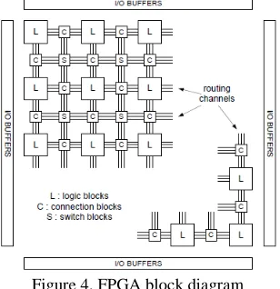
FPGA consists of thousands of universal building blocks, known as configurable logic blocks (CLBs), connected using programmable interconnects. Reconfiguration is able to change a function of each CLB and connections among them, leading to a functionally new digital circuit Fig 4.Figure 4. FPGA block diagram
For implementing cryptography in hardware, FPGAs provide the only major alternative to custom and semicustom Application Specific Integrated Circuits (ASICs). Integrated circuits that must be designed all the way from the behavioral description to the physical layout are sent for an expensive and time-consuming fabrication. The implementation of the AES algorithm based on FPGA devices has the following advantages over the implementation based on ASICs:
• Shorter design cycle leading to fully functioning device.
• Lower cost of the computer-aided design tools, verification and testing.
• Potential for fast, low-cost multiple reprogramming and experimental testing of a large number of various architectures and revised versions of the same architecture.
• Higher accuracy of comparison: in the absence of the physical design and fabrication, ASIC designs are compared based on inaccurate pre-layout simulations [6]; FPGA designs are compared based on very accurate post- layout simulations and experimental testing.
There are several FPGA families available in the market; Altera Stratix II and Cyclone II families, Atmel AT6000 and AT40K families, Lattice LatticeEC and LatticeECP families and Xilinx Spartan-3 and Virtex families we have chosen a Virtex family from Xilinx, Inc. in this paper for implementing AES algorithm.
IV.PROGRAMMING FPGA
Different techniques for programming FPGAs (i.e. to load the configuration bits into SRAM cells) were identified in the open literature. The simplest one is to connect all the bits into a long shift register. This requires only one pin to input the programming data but is the slowest method. Faster configuration speeds are obtained by organizing programming bits into memories and to manage them as parallel data. But software like Xilinx or Altera is used to program FPGA through devices like Spartan and Vertex. The standard FPGA design flow in Fig 5 starts with design entry using schematics or a hardware description language (HDL), such as Verilog HDL or VHDL. In this step, you create the digital circuit that is implemented inside the FPGA. The flow then proceeds through compilation, simulation, programming, and verification in the FPGA hardware.
Steps for designing FPGA:
© 2013, IJCSMC All Rights Reserved
608
3. Generate a UCF file to hold constraints such as pin assignments. Use the PlanAhead tool to generate this file.4. Assign the I/O pins in your design to the pins on the FPGA that you want them connected to. 6. Implement the design to map it to the specific FPGA on the Spartan-3E board.
7. Generate the programming .bit file that has the bitstream that configures the FPGA.
8. Connect Spartan3 board to the computer and use the iMPACT tool to program the FPGA using the bitstream.
V. SIMULATING RESULT
The design has been coded by VHDL and results shown in figure below are synthesized and simulated basing on the Xilinx ISE design suite and Xilinx ISim simulation is used for simulating. Encryption simuation is shown in figure and decryption simulation is shown in figure.
Encryption:
The simulation results of full encryption module is shown in Fig 6 where input vectors and keys are given from FIPS 197 [1] and output was verified.
Input Plain text: 00112233445566778899aabbccddeeff Input Cipher Key: 000102030405060708090a0b0c0d0ef
Figure 6. Encryption
Decryption:
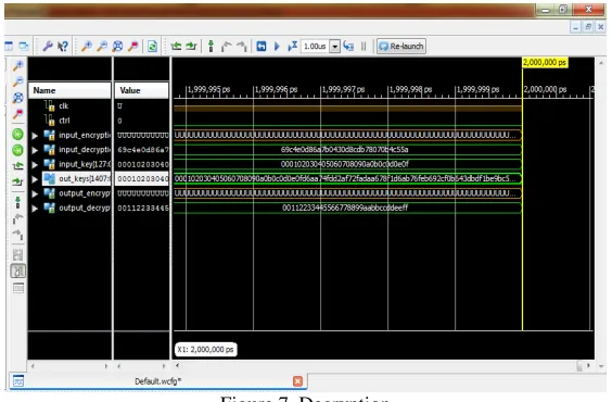
The simulation results of full encryption module is shown in Fig 7 where input vectors and keys are given from FIPS 197 [1] and output was verified.
Input Cipher text: 69c4e0d86a7b0430d8cdb78070b4c55a Input Cipher Key: 000102030405060708090a0b0c0d0ef
© 2013, IJCSMC All Rights Reserved
609
VI.CONCLUSIONThe Advanced Encryption Standard algorithm is a symmetric block cipher that can process data blocks of 128 bits through the use of cipher keys with lengths of 128, 192, and 256 bits. An efficient FPGA implementation of 128 bit block and 128 bit key AES algorithm has been presented in this paper. The design is implemented on Xilinx using Spartan 3E FPGA. The design is tested with the sample vectors provided by FIPS 197 [1]. Future work will be to implement this algorithm on hardware and perform power analysis attack to find the secret key.
REFERENCES
[1] National Inst. Of Standards and Technology, “Federal Information Processing Standard Publication 197, the Advanced Encryption Standard (AES),” Nov. 2001
[2] J. Daemen and V. Rijmen,” AES Proposal: Rijndael,” AES Algorithm Submission, Sept. 1999
[3] William Stallings, Cryptography and Network Security, Principles and Practices, 4th ed. Pearson Education, pp. 134-161, 2006
[4] Charlie Kaufman, Radia Perlman, Mike Speciner, Network Security, Private Communication in a Public World, 2nd ed. Pearson Education, pp. 41-114, 2006
[5] DAEMEN, J.—RIJMEN, V. : AES Proposal: Rijndael, The Rijndael Block Cipher, AES Proposal, pp. 1–45, 1999 (http://csrc.nist.gov/CryptoToolkit/aes/).
[6] Wayne Wolf, “FPGA-Based System Design, Pearson Education, pp. 17-37
[7] Tessier, R., and Burleson, W., “Reconfigurable computing for digital signal processing: a survey”, J.VLSI Signal Process., 2001, 28, (1-2), pp.7-27.
[8] Ahmad, N.; Hasan, R.; Jubadi, W.M; “Design of AES S-Box using combinational logic optimization”, IEEE Symposium on Industrial Electronics & Applications (ISIEA), pp. 696-699, 2010.
[9] Daemen J., and Rijmen V, "The Design of Rijndael: AES-the Advanced Encryption Standard", Springer-Verlag, 2002