LOW POWER DIGITAL IMAGE PROCESSING USING
APPROXIMATE ADDERS
Varsha S Kumar
1, U.Hari
21
M Tech [VLSI], Dept. of ECE, SRM University,Chennai, Tamilnadu, (India)
2
Assistant professor (SG),Dept. of ECE, SRM University,Chennai, Tamilnadu, (India)
ABSTRACT
Low power is one of the emerging trend in the field of VLSI which can be used in portable multimedia devices employing various signal processing algorithms and architectures. In most multimedia applications, human beings can gather useful information from slightly erroneous outputs. Therefore, we do not need to produce exactly correct numerical outputs. So we are using different approximate adders to implement this algorithm in image processing and video processing. Approximate adders with reduced complexity are used in designing this algorithm and the techniques result in significantly shorter critical paths. The proposed adders can achieve significant throughput improvement and total power reduction over conventional adder designs.
Keywords:
Approximate Computing, Adder Design, Low Power, PSNR .
I INTRODUCTION
Digital signal processing (DSP) blocks form the Backbone of various multimedia applications used in Portable devices. Most of these DSP blocks implement image and video processing algorithms, where the ultimate output is either an image or a video for human consumption. Human Beings have limited perceptual abilities when interpreting an Image or a video. This allows the outputs of these algorithms to be numerically approximate rather than accurate. This Relaxation on numerical exactness provides some freedom to carry out imprecise or approximate computation. We can use this freedom to come up with low-power designs at different levels of design abstraction, namely, logic, architecture, and algorithm.
probabilistic CMOS (PCMOS), and implement efficient arithmetic using PCMOS. Shin et al. [11] propose a logic synthesis approach to design an approximate circuit.
II APPROXIMATE ADDERS
Various approximate adders are previously designed to reduce logical complexity and to reduce critical path. In section 2 we are designing a digital approximate adder which cut the carry chain and thus reduce the critical path delay. In section 3 we are designing various approximate adders which reduces complexity in transistor level. Which reduces critical path delay and power? Section 4 we are discussing about image processing algorithm using these approximate adders
III IMPLEMENTATION OF APPROXIMATE ADDER
Previous approximate adders have difficulty detecting and correcting errors since they are designed for error-acceptable applications with target accuracy. However, accurate computations are still required at certain times, according to the application. VLSA can provide accurate results, but has large delay and area overhead for the error detection and correction.
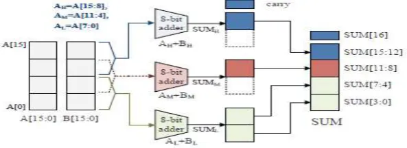
Fig. 1 Proposed Approximate Adder – 16-Bit Adder Case Delay
The central contribution of our present work is to propose an approximate adder which supports both accurate and inaccurate computation with error-correction and accuracy-configuration capability. Figure 1shows our proposed approximate circuit for the case of a 16-bit adder. In the adder, the carry chain is cut to reduce critical-path delay, and three sub-adders generate results of partial summations. With the reduced critical-critical-path delay, high performance (by increasing the clock frequency) or low power consumption (by decreasing the operating voltage) is obtained. A middle adder (AM+BM) is introduced to increase accuracy. Without the middle sub-adder error occurs when the eighth carry bit is high, and for random input patterns the error rate is 50.1%. On the other hand, with the introduction of the middle sub-adder, error rate for random input patterns is reduced to 5.5%. (In the real implementation, all redundant parts (four-LSB output of AH + BH and AM + BM sub-adders) are optimized only for carry-generation.)
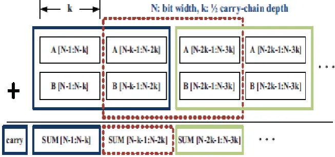
Fig. 2 General implementation for the proposed adder.
The approximate adder thus consists of the (N/k−1) sub-modules as described in Equation (1).
SUM[N-ik-1:N-(i+1)k]=
A[N-ik-1 : N-(i+2)k]+
B[N-ik-1 : N-(i+2)k],
where i=0,…..N/k – 2 (1)
In modern adder designs, such as carry-look ahead (CLA), carry select and Kogge-Stone adders, the path depth and area are asymptotically proportional to log2N and Nlog2N respectively, where N is the bit-width of the adder. Based on this, we can express delay, area and power consumption of the proposed adder in terms of the parameters N and k. The proposed ACA adder has (N/k − 1) sub-adders, each of which is a 2k-bit adder.
Therefore, delay of the critical path can be expressed with Equation (2) and area can be estimated with Equation (3), where Cdelay and Carea are constants for delay and area, respectively.
Delay =𝐶𝑑𝑒𝑙𝑎𝑦(𝑙𝑜𝑔2𝑘 + 1) (2)
Area =𝐶𝑎𝑟𝑒𝑎 (𝑁 − 2𝑘)(𝑙𝑜𝑔2k + 1) (3)
𝑃𝑜𝑤𝑒𝑟𝑑𝑦𝑛=𝐶𝑝𝑜𝑤𝑒𝑟(N-2k)(𝑙𝑜𝑔2k + 1) (4)
Power consumption of the ACA adder can be roughly estimated as follows. Dynamic power consumption with voltage scaling at a fixed frequency is proportional to capacitance · ß 𝑉𝑑𝑑2 where the capacitance is
proportional to the area. Cell delay is proportional to 1/(𝑉𝑑𝑑 − 𝑉𝑡ß) and 𝑉𝑑𝑑2 is roughly proportional to 1/ (cell
delay) if we assume that is 2. Since (cell delay) × (path depth) is constant at a fixed frequency, 𝑉𝑑𝑑2is proportional to the path depth, which is log2k + 1. Consequently, dynamic power with voltage scaling can be expressed using Equation (4), where Cpower is a constant fixed for given Vdd for dynamic power consumption. Static power consumption of the adder can be roughly estimated as proportional to the area in Equation (3).
result will be correct when there are no errors in all (N/k − 1) sub-adders. In the ith sub-adder, errors occur when the LSB part of the result (SUMi[k − 1 : 0]) has all „1‟ values (probability P = 1/2k ) and the LSB part ([k − 1 :
0]) of the (i + 1)th sub-adder produces a carry bit (probability P=(1/4+1/2 .1/4+1/2.1/2.1/4+…..)
Therefore, with a random input vector, the probability of having a correct result in the proposed adder is
𝑃 𝑁, 𝑘 = (1 −21𝑘.22𝑘𝑘+1−1)𝑁𝑘−2 (5)
.
IV APPROXIMATE ADDERS
In this we are implementing various approximate adders using mirror adder logic. We are removing transistors from this adder and constructing approximate adders
.
4.1 Approximation strategies for the mirror adder In this section, we explain step-by-step procedures for coming up with various approximate MA cells with fewer transistors. Removal of some series connected transistors will facilitate faster charging/discharging of node capacitances. Moreover, complexity reduction by removal of transistors also aids in reducing the αC term (switched capacitance) in the dynamic power expression
Pdynamic = αCV2DDf
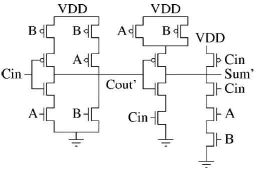
4.1.1 Approximation 1: In order to get an approximate MA with fewer transistors, we start to remove transistors from the conventional schematic one by one. However, we cannot do this in an arbitrary fashion. We need to make sure that any input combination of A,B and Cin does not result in short circuits or open circuits in the simplified schematic. Another important criterion is that the resulting simplification should introduce minimal errors in the FA truth table. A judicious selection of transistors to be removed (ensuring no open or short circuits) results in a schematic shown in Fig. 3.2, which we call approximation 1. Clearly, this schematic has eight fewer transistors compared to the conventional MA schematic. In this case, there is one error in Cout and two errors in Sum.
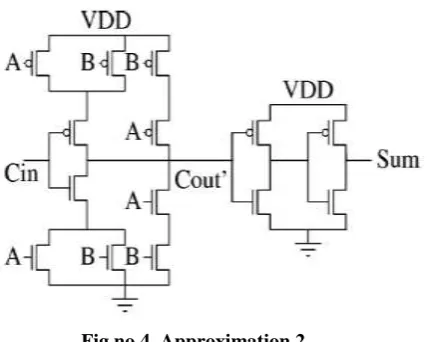
4.1.2 Approximation 2: The truth table of an FA shows that Sum= Cout for six out of eight cases, except for the input combinations A = 0,B = 0,Cin = 0 and A = 1,B = 1,Cin = 1. Now, in the conventional MA, Cout is computed in the first stage. Thus, an easy way to get a simplified schematic is to set Sum= Cout. However, we introduce a buffer stage after Cout to implement the same functionality. The reason for this can be explained as follows. If we set Sum= Cout as it is in the conventional MA, the total capacitance at the Sum node would be a combination of four source–drain diffusion and two gate capacitances. This is a considerable increase compared to the conventional case or approximation 1. Such a design would lead to a delay penalty in cases where two or more multi-bit approximate adders are connected in series, which is very common in DSP applications. Fig. 3 shows the schematic obtained using the above approach. We call this approximation2. Here, Sum has only two errors, while Cout is correct for all cases.
Fig no 4 Approximation 2
4.1.3 Approximation 3:Further simplification can be obtained by combining approximations 1 and 2. Note that this introduces one error in Cout and three errors in Sum.
Fig no 5Approximation 3
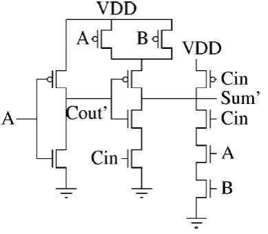
Fig no 6 Approximation 4
Table 1 Truth Table For Conventional FA And Approx 1-4
V IMAGE COMPRESSION
In Section 2 and 3, approximate FA cells were introduced. Using these approximate FA cells also introduces errors in FA. When approximate FA cells are used to design multi-bit adders, the outputs of these adders will be erroneous. Multimedia DSP algorithms mostly consist of additions and multiplications. Multiplications can be treated as shifts and adds. Therefore, adders can be considered as basic building blocks for these algorithms. Interestingly, most DSP algorithms used in multimedia systems are characterized by inherent error tolerance. Hence, occasional errors in intermediate outputs might not manifest as a substantial reduction in the final output quality. We focus on image compression algorithms, and present the results of using our approximate FA cells in these algorithms.
5.1 DCT The DCT and inverse discrete cosine transform (IDCT) are integral components of a Joint Photographic Experts Group (JPEG) image compression system. One-dimensional integer DCT y (k) for an eight-point sequence x (i) is given
y(k) = a k, i x i , k = 0,1, … .7 7
i=0
integer coefficients a(k, i), k = 1, . . . , 7 so that the multiplication a(k, i)x(i) is converted to two left shifts and an addition (using an RCA(Ripple carry adder). Since a(0, i) corresponds to the dc coefficient, which is most important, we leave it unaltered. The multiplication a(0, i)x(i) then corresponds to an addition of four terms. This is done using a carry-save tree using a 4:2 compressor followed by an RCA. Also, each integer DCT and IDCT output is the sum of eight terms. Thus, these outputs are calculated using a carry-save tree using an 8:2 compressor followed by an RCA. Thus, the whole DCT–IDCT system now consists of RCAs and CSAs(carry save adder). In our design, all RCAs and CSAs are approximate, which use the approximate FA cells proposed earlier
DIGITAL APPROXIMATE ADDER
5.2. Output Quality
: We measure the output quality of the decoded image after IDCT using the well-known metric of peak signal-to-noise ratio (PSNR). The output PSNR for the base case is 31.16 dB.5.2.1PSNR Many signals have a very wide dynamic range, (ratio between the largest and smallest possible values of a changeable quantity) the PSNR is expressed in terms of the logarithmic decibel scale. Using PSNR value for the same set of tests images, different image enhancement algorithms can be compared systematically to identify whether a particular algorithm produces better results. The dimensions of the correct image matrix and the dimensions of the degraded image matrix must be identical.
The mathematical representation of the PSNR is as follows:
𝑃𝑆𝑁𝑅 = 20 log10(
𝑀𝐴𝑋𝑓
𝑀𝑆𝐸)
Where MSE is the Mean Squared Error.
𝑀𝑆𝐸 = 1
𝑚𝑛 ||𝑓 𝑖, 𝑗 − 𝑔(𝑖, 𝑗)||2
𝑛−1
0 𝑚 −1
0
This can also be represented in a text based format as: MSE = (1/(m*n))*sum(sum((f-g).^2))
PSNR = 20*log(max(max(f)))/((MSE)^0.5) Legend:
f represents the matrix data of our original image
g represents the matrix data of our degraded image in question
m represents the numbers of rows of pixels of the images and i represents the index of that row n represents the number of columns of pixels of the image and j represents the index of that column MAXf is the maximum signal value that exists in our original image
VI RESULTS
The Low Power Digital Image Processing Using Approximate Adder is implemented in Verilog programming language, MATLAB and simulated. It has been synthesized and implemented by Xilinx ISE 12.3tools.The results are shown in the table 2. Power is reduced and image quality is maintained.
Adders Digital
approximate
adder
Approximation 1 Approximation 2 Approximation 3 Approximation 4
PSNR 32.2 30.12 24.56 34.44 35.56
power 160.mw 163.mw 160.mw 156.mw 154mw
Table 2 Power and PSNR Comparison
VII CONCLUSION
transform is applied row ways and column ways to input image to get the transformed values. Then image is reconstructed using inverse discrete cosine transform. Power and area are reduced while using approximate adder. Image quality is maintained.
REFERENCES
[1] Vaibhav Gupta, Debabrata Mohapatra, Anand Raghunathan, Fellow, IEEE, and Kaushik Roy, Fellow, IEEE, Low-Power Digital Signal Processing Using Approximate Adders, IEEE TRANSACTIONS ON COMPUTER-AIDED DESIGN OF INTEGRATED CIRCUITS AND SYSTEMS, VOL. 32, NO. 1, JANUARY 2013
[2] V. Gupta, D. Mohapatra, S. P. Park, A. Raghunathan, and K. Roy,IMPACT: Imprecise adders for low-power approximate computing,” in Proc. IEEE/ACM Int. Symp. Low-Power Electron. Design, Aug. 2011 [3] A. K. Verma, P. Brisk, and P. Ienne, “Variable latency speculative addition: A new paradigm for
arithmetic circuit design,” in Proc. Design, Automat. Test Eur., 2008,
[4] P. Kulkarni, P. Gupta, and M. D. Ercegovac, “Trading accuracy for power in a multiplier architecture,” J. Low Power Electron., vol. 7, no. 4, pp. 490–501, 2011
[5] Accuracy-Configurable Adder for Approximate Arithmetic Designs Andrew B. Kahng and Seokhyeong Kang ECE and CSE Departments, University of California
[6] D. Shin and S. K. Gupta, “A Re-Design Technique for Datapath Modules inError Tolerant Applications”, Proc. Asian Test Symp., 2008, pp. 431–437
[7] S.-L. Lu, “Speeding Up Processing with Approximation Circuits”, IEEE Computer 37(3) (2004) pp. 67-73. [8] A. K. Verma, P. Brisk and P. Ienne, “Variable Latency Speculative Addition: A New Paradigm for
Arithmetic Circuit Design”, Proc. DATE, 2008, pp. 1250–1255.
[9] N. Zhu, W. Goh and K. Yeo, “An Enhanced Low-Power High-Speed Adder For Error-Tolerant Application” Proc. Intl. Symp. on Integrated Circuits, 2009, pp. 69–72.
[10] N. Zhu, W. Goh, W. Zhang, K. Yeo and Z. Kong, “Design of Low-Power High-Speed Truncation-Error-Tolerant Adder and Its Application in Digital Signal Processing”, IEEE Trans. on VLSI Systems 18(8)
(2010), pp. 1225–1229.
[11] D. Shin and S. K. Gupta, “Approximate Logic Synthesis for Error Tolerant Applications”, Proc. DATE,
2010, pp. 957–960.
Authors
Varsha S Kumar has completed her B.Tech. in Electronics & Communication Engineering Branch in 2012 from Cochin University of Science and Technology, Kerala. She is pursuing her M.Tech in VLSI Design from SRM University, Chennai, Tamil Nadu. At present she is in the 4th and final Semester of M.Tech.