IJEDR1503054 International Journal of Engineering Development and Research (www.ijedr.org) 1
Reduction of Leakage Power in CMOS circuits
(Gates) using LC nMOS Technique
Abhishek Verma1, Vishal Ramola2,
M.Tech. Student of VLSI Design Department, UTU Dehradun, UK India1
Assist. Prof. VLSI Design Department, UTU, Dehradun, UK India2
________________________________________________________________________________________________________
Abstract - Leakage Power is the major problem in digital circuits. There are various techniques to reduce the leakage power technique. One technique discussed in this paper. We propose a technique called LCnMOS for designing logic gates which significantly cuts down the leakage current without increasing the dynamic power dissipation. LCnMOS, a technique to tackle the leakage problem in logic gate circuits, uses single additional leakage control transistor, driven by the output from the pull up and pull down networks, which is placed in a path from pull down network to ground which provides the additional resistance thereby reducing the leakage current in the path from supply to ground. All the performance has been investigated using 90nm and 180nm Technology at 1 voltage and evaluated by the comparison of the simulation result obtain from TSPICE.
Keywords - Leakage control Transistor nMOS, Delay, leakage power, LECTOR Technique
________________________________________________________________________________________________________
I. INTRODUCTION
With the increasing prominence of portable systems, it is important to prolong the battery life as much as possible, since it is the limited battery life time that typically imposes strict demands on the overall power consumption of such systems. Although the battery industry has been making efforts to develop batteries with a higher energy capacity than that of conventional Nickel-Cadmium (NiCd) batteries, a revolutionary increase of the energy capacity does not seem imminent. Therefore, portable applications have led to rapid and innovative developments in low-power circuit designs. Power dissipation is also crucial for Deep Sub- Micron (DSM) technologies [1]. To further improve the performance of the circuits and to integrate more functions on a chip, the feature size has to continue to shrink. As a result, the power dissipation per unit area grows, increasing the chip temperature. Although power dissipation is important for modern VLSI design, performance, speed and area are still the main requirements of a design. However, low-power design usually involves making tradeoffs such as timing versus power and area versus power. Increasing performance, while the power dissipation is kept constant, is also considered to be a low-power design problem.
In fact, higher performance-per-watt is the new technique for micro-processor chip manufacturers today. In order to achieve high density and high performance, CMOS technology feature size and threshold voltage have been scaling down for decades. Because of this trend, transistor leakage power has increased exponentially. The reduction of the supply voltage is dictated by the need to maintain the electric field constant on the ever shrinking gate oxide.
The paper is organized as follows: in Section II, previous work is reviewed. Subsequently, in section III, the modified Low power logic gates with LCnMOS approach are presented. In section IV, the simulation results are given and discussed. The comparison and evaluation for modified and existing designs are carried out. Finally a conclusion will be made in the last section.
II. PRELIMINARIES
(A) Sleep Transistor Technique
This is a State-destructive technique which cuts off either pull-up or pull-down or both the networks from supply voltage or ground or both using sleep transistors. This technique is MTCMOS, which adds high-Vth sleep transistors between pull-up networks and Vdd and pull down networks and Gnd while for fast switching speeds, low-Vth transistors are used in logic circuits [2]. This technique dramatically reduces leakage power during sleep mode. However, the area and delay are increased due to additional sleep transistors. During the sleep mode, the state will be lost as the pull-up and pull-down networks will have floating values. These values impact the wakeup time and energy significantly due to the requirement to recharge transistors which lost state during sleep.
(B) Sleepy Keeper Technique [3]
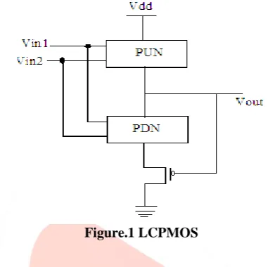
IJEDR1503054 International Journal of Engineering Development and Research (www.ijedr.org) 2 Figure.1 LCPMOS
(E) Proposed LCnMOS
In this proposed technique, we introduce a single leakage control transistor within the logic gate for which the gate terminal of leakage control transistor (LCT) is controlled by the output of the circuit itself. Which increases the resistance of the path from pull down network to ground thereby increasing the resistance from Vdd to ground, leading to significant decrease in leakage currents? The main advantage as compared to other techniques is that LCnMOS technique does not require any additional control and monitoring circuitry, thereby limits the area and also the power dissipation in active state.
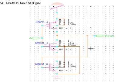
Leakage Control nMOS (LCnMOS) technique is illustrated in detail with the case of an inverter. A LCnMOS inverter is shown in Figure 2. An nMOS is introduced as LCT between M1 and Gnd nodes of inverter. When Vdd=1V, input A=0, the output is high. As the output drives the LCT the LCT goes to ON state hence provides high resistance path between Vdd and Gnd. When A=1, the output is low; hence LCT will be in OFF state hence output is low. LCnMOS inverters for all possible inputs are tabulated in Table 1.
Table-1
In the sleep related technique, the sleep transistors have to be able to isolate the power supply and/or ground from the rest of the transistors of the gate. Hence, they need to be made bulkier dissipating more dynamic power. This offsets the savings yielded when the circuit is idle. Sleep transistor technique depends on input vector and it needs additional circuitry to monitor and control the switch in sleep transistors, consuming power in both active and idle states. In comparison, LC nMOS generates the required control signals within the gate and is also vector independent.
Single transistor is added in LC nMOS technique in every path from Vdd to Gnd irrespective of number of transistors in pull-up and pull-down network. The loading requirement with LCT is a constant which is much lower.
IJEDR1503054 International Journal of Engineering Development and Research (www.ijedr.org) 3 Figure 2. LC nMOS based CMOS Inverter
III. APPLYING LCNMOS TO CMOS CIRCUITS
Various circuit applications of the LCnMOS technique are explored in this section. The LCnMOS technique is applied to the following CMOS circuits and also the irrespective base case are implemented to calculate the amount of leakage power reduced in LCnMOS technique.
(A) LCnMOS based NOT gate
Figure 3. LC nMOS based NOT gate
IJEDR1503054 International Journal of Engineering Development and Research (www.ijedr.org) 4 Figure 4 Simulation Waveform of LCnMOS Inverter
(B) LCNMOS based NAND gate
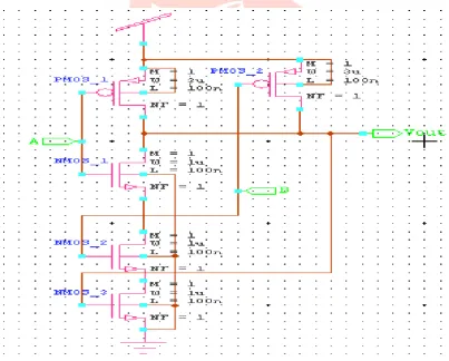
The 2-input CMOS NAND gate is shown in Figure7with the one LCT added between pull-down network and gnd. The simulation wave forms of LCnMOS NAND from Figure5 show that the basic characteristics of NAND are retained by LCnMOS NAND.
IJEDR1503054 International Journal of Engineering Development and Research (www.ijedr.org) 5 Figure.6:Simulation waveforms of LCnMOS NAND gate
(C) LCnMOS based NOR gate
The 2-input CMOS NOR gate is shown in Figure7 with the one LCT added between pull-down network and gnd. The simulation waveforms of LCnMOS NOR from Figure8 show that the basic characteristics of NOR are retained by LCnMOS NOR gate
.
IJEDR1503054 International Journal of Engineering Development and Research (www.ijedr.org) 6 Figure.8:Simulation waveforms of LCnMOS NOR gate
IV EXPERIMENTAL RESULTS
The leakage power is measured using the Tanner Tool S-EDIT simulator. The results obtained through the technique for logic gates are shown in Table 2. Simulation for the logic gates are performed by taking two different process parameters Viz.180nm, 90nm CMOS Technology.
Table-2
CONCLUSION
In this paper we have presented leakage power reduction LCnMOS technique. It becomes a great challenge to tackle the problem of leakage power. LCnMOS uses one LCT which is controlled by the output of circuit itself. LCnMOS achieves the reduction in leakage power compared to other leakage reduction techniques, such as LECTOR, sleep transistor, sleepy keeper, etc. The performance has been investigated using 180nm & 90nm Technology and evaluated by the comparison table 2 of the simulation result obtain from TSPICE.
REFERENCES
[1] John F. Wakerly, “Digital Design- Principles and Practices” , fourth edition [2] M. D. Powell, S. H. Yang, B. Falsafi, K. Roy, and T. N.
IJEDR1503054 International Journal of Engineering Development and Research (www.ijedr.org) 7 [3] S. H. Kim and V. J. Mooney, “Sleepy Keeper: a new approach to low-leakage power VLSI design,” IFIP, pp. 367-372, 2006. [4] Bagadi Madhavi, G Kanchana, Venkatesh Seerapu “Low Power and Area Efficient Design of VLSI Circuits” International Journal of Scientific and Research Publications, Volume 3, Issue 4, April 2013, ISSN 2250-3153.
[5] B. S. Deepak subramanyan and A. Nunez, “Analysis of Sub threshold Leakage Reduction in CMOS Digital Circuits,” Proceedings of the 13th NASA VLSI Symposium, Post Falls, 5-6 June 2007, pp. 1-8.
[6] R. X. Gu and M. I. Elmasry, “Power Dissipation Analysis
and Optimization of Deep Submicron CMOS Digital Circuits” IEEE Journal of Solid-State Circuits, Vol. 31, No. 5, 1996, pp. 707-713. http://dx.doi.org/10.1109/4.509853.
[7] D. Lee, W. Kwong, D. Blaauw and D. Sylvester, “Analysis and Minimization Techniques for Total Leakage considering Gate Oxide Leakage" In Proceedings of the 40th Design Automation Conference, pp. 175-180, Anaheim, 2003.
[8] P. Verma, R. A. Mishra, “Leakage power and delay analysis of LECTOR based CMOS circuits”, Int’l conf. on computer & communication technology ICCCT 2011.
[9] Kaushik Roy, Saibal Mukhopadhyay and hamid mahmoodi-meimand “Leakage Current Mechanisms and Leakage Reduction Techniques in Deep-Sub micrometer CMOS Circuits” in IEEE, Vol. 91, no. 2, Feb 2003.
[10] N. Hanchate and N.Ranganathan, “LECTOR: A Technique for leakage reduction in CMOS circuits”, IEEE Trans. VLSI Systems, vol. 12, pp.196-205, Feb., 2004.
[11] B. Dilip, P. Surya Prasad,” Design of Leakage Power Reduced Static RAM using LECTOR”, in journal (IJCSIT) International Journal of Computer Science and Information Technologies, Vol. 3 (3).