IJEDR1402177
International Journal of Engineering Development and Research (www.ijedr.org)2396
Abstract-This work presents the proposed diode assisted VSI enhances the voltage boost capability which is suitable for wide range voltage regulation in DC to AC power conversion. This project mainly concentrates on the PWM techniques for the diode assisted VSI. Improved PWM strategies demonstrates good performances: less switching device requirement and higher efficiency at high voltage gain. This PWM technique is theoretically studied and analysed for diode assisted and simulation results are validated through Mat lab 2013a.Keyword- SPWM, Boost converter, VSI, Diode Assisted Network
________________________________________________________________________________________________________
I.INTRODUCTION
For sustainable development of economy and environment, solar cells and fuel cells as clean energy are promising in various power electronic applications. Photovoltaic generated system and fuel cells supplied to motor drive systems. The obvious characteristic in these applications is low dc source voltage supply with wide range voltage drop and required high AC output voltage. In hybrid electric vehicles drive system, the AC output voltage should be converted from zero to the rated voltage in order to achieve the high constant power or the maximum torque capability over a wide range of operation. These application raise new requirements for power electronic converters such as the capability of wide range voltage buck-boost and high efficiency.[1-3]
In conventional VSI having the output voltage lower than the DC input voltage or equal to the 1.15 times the DC input voltage. For requiring both voltage boost power conversion conventional two stage DC-DC boosted VSI has been widely used because of its simple structure and mature control technology. Due to additional power Conversion stage increasing system cost and lowing efficiency.
II.DIODEASSISTEDBOOSTVOLTAGESOURCEINVERTER
In industry it is well known that conventional voltage source inverter (VSI) has a limitation in the sense that it can only perform voltage buck operation with its peak ac output voltage always less than or equal to 1.15 times the constant dc input voltage. For application like renewable energy harnessing where the input voltage fluctuates over a wide range voltage boost operation is might, at times, be needed for stabilizing the ac output voltage at a desired value. To achieve this DC to DC boost converter and Z-Source can be use but it has some limitation compare to the Diode Assisted Boost VSI.
The diode-assisted capacitor network introduces an instantaneous intermediate dc-link voltage change of the inverter bridge in one switching time period. However, the PWM strategies presented just utilize active vectors for ac output in the duration when the two capacitors are connected in series. When the switching device SW is turned OFF, the two capacitors are connected in parallel through two forward-biased diodes and the intermediate dc-link voltage Vin is the same as the capacitor voltage. During this interval, the three-phase VSI operates in null state and output ac voltage is zero. In view of the variable intermediate dc-link voltage of the inverter bridge in one switching time period, sufficient utilization of intermediate dc link voltage can improve the voltage transfer ratio and reduce the voltage rating of the capacitors.[2,3]
IJEDR1402177
International Journal of Engineering Development and Research (www.ijedr.org)2397
Fig.1 Diode Assisted Boost Voltage Source Inverter.Above fig.1 shows the circuit diagram for diode assisted boost inverter. In that we show the boost inductor then switch SW then diode capacitor network and then inverter.Diode Assisted Boost VSI has two operating modes according to the switching states of SW. For the convenience of analysis, the two capacitors C1 and C2 in the symmetrical X-shaped are assumed to have the same capacitance and terminal voltages .[3-7]
A.When Switch SW Is On
When switch SW is turned ON, during this interval the two Diodes are reverse biased as shown in fig.2 Therefore, the inductor absorbs energy from the DC source by increasing the charging current and both of the capacitors are connected in series to supply the loads. [5-7]
Fig.2 Diode Assisted Boost VSI when Switch SW is ON. (1)
( ) (2) B.When Switch SW Is Off
When switch is turned OFF, during this the two diodes are forward biased. Therefore, the energy stored in inductor is transferred to the capacitors and both capacitors are connected in parallel to supply the loads.[5-7]
IJEDR1402177
International Journal of Engineering Development and Research (www.ijedr.org)2398
Similarly, the average intermediate dc-link voltage across the inverter bridge can be written as follows: ( )
( ) ………(8)
IV.INDUCTORDESIGN[10,11]
Here we are having the boost inductor so that calculation should apply for this inductor which is used in normal Boost Converter. Here, we need boost voltage double of the input voltage.
Input DC voltage Weneed output voltage Vac = 48V. Duty cycle
………(9)
………..(10) Now, boost inductor L,
( ) ……….(11) ……….(12) .
V.CAPACITORDESIGN[10,11]
Here we are having the two symmetrical capacitors and normal boost converter equations should applying. ………..(13) ………..(14) ………(15) .
VI.IMPROVEDSINEPULSEWIDTHMODULATION[6-9]
IJEDR1402177
International Journal of Engineering Development and Research (www.ijedr.org)2399
Fig.4 Generating pulses for three phase inverterAbove fig.5.2 shows the comparison between the carrier and sine wave to generate the inverters gate pulses. With the help of this comparison we get the eight switching states in this two zero states and six active states. And in this two zero states we are applying the pulse to the switch SW.
Fig.5 Generating Pulses for Switch SW
As shown in above fig.5.2b we can see that we are comparing the carrier signal with the two constant signal. With the help of this we can apply the pulses to the switch SW which are zero states of the inverters.
TABLE NO.I MATLAB PARAMETER FOR SIMULATION
Parameters Values
DC input Voltage 24 V Inductance L 0.135 mh Capacitance C1 and C2 2.6 𝜇F Load Resistance R1, R2 and R3 30 Ω
Switching Frequency 10,000 Hz
VII.SIMULATIONRESULTS
IJEDR1402177
International Journal of Engineering Development and Research (www.ijedr.org)2400
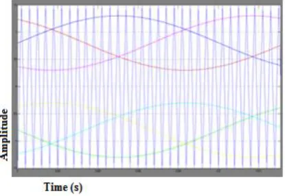
Fig.7 Output Phase currentVIII.CONCLUSION
In this project we have analysed improved Sine PWM technique and apply it in matlab. With the help of Diode Assisted VSI we can enhance the voltage boost capability which is suitable for wide range voltage regulation in DC to AC power
conversion. With an improved SPWM strategy with high dc-link voltage utilization is using to obtain the maximum voltage
gain.
REFERENCES
[1] F. Z. Peng, “Z-Source inverter,” IEEE Trans. Ind. Appl., vol. 39, no. 2,pp. 504–510, Mar. 2003.
[2] F. Gao, P. C. Loh, R. Teodorescu, and F. Blaabjerg, “Diode-assisted buck–boost voltage-source inverters,” IEEE Trans. Power Electron., vol. 24,no. 9, pp. 2057–2064, Sep. 2009.
[3] Maximum Boost Control of the Z-Source Inverter Fang ZhengPeng, Fellow, IEEE, MiaosenShen, Student Member, IEEE, and ZhaomingQian, Senior Member, IEEE.
[4] Comparison of Traditional Inverters andZ-Source Inverter for Fuel Cell Vehicles.MiaosenShen, Member, IEEE, Alan Joseph, Jin Wang, Member, IEEE, Fang Z. Peng, Fellow, IEEE, and Donald J. Adams
[5] Constant Boost Control of the Z-Source Inverter to Minimize Current Ripple and Voltage Stress.MiaosenShen, Student Member, IEEE, Jin Wang, Member, IEEE, Alan Joseph, Fang ZhengPeng, Fellow, IEEE, Leon M. Tolbert, Senior Member, IEEE, and Donald J. Adams, Member, IEEE.
[6] Improved pwm strategies for diode assisted buck-boost voltage source inverter.
[7] Yan Zhang, Student Member, IEEE, Jinjun Liu, Senior Member, IEEE, and Chaoyi Zhang.
[8] M.-K. Nguyen, Y.-C. Lim, and G.-B. Cho, “Switched-inductor quasi-Zsource inverter,” IEEE Trans. Power Electron., vol. 26, no. 11, pp. 3183–3191, Nov. 2011.
[9] L.-S. Yang, T.-J. Liang, and J.-F. Chen, “Transformerless dc–dc converters with high step-up voltage gain,” IEEE Trans. Ind. Electron., vol. 56, no. 8, pp. 3144–3152, Aug. 2009.