Gallium Nitride Materials—Progress, Status,
and Potential Roadblocks
ROBERT F. DAVIS, AMY M. ROSKOWSKI, EDWARD A. PREBLE, JAMES S. SPECK,
BEN HEYING, JAIME A. FREITAS, Jr., EVAN R. GLASER,
ANDWILLIAM E. CARLOS
Invited Paper
Metal–organic vapor phase epitaxy (MOVPE) and molecular beam epitaxy (MBE) are the principal techniques for the growth and n-type (Si) and p-type (Mg) doping of III-nitride thin films on sapphire and silicon carbide substrates as well as previously grown GaN films. Lateral and pendeoepitaxy via MOVPE reduce significantly the dislocation density and residual strain in GaN and AlGaN films. However, tilt and coalescence boundaries are produced in the laterally growing material. Very high electron mobilities in the nitrides have been realized in radio-frequency plasma-assisted MBE GaN films and in two-dimensional electron gases in the AlGaN/GaN system grown on MOVPE-derived GaN substrates at the crossover from the intermediate growth regime to the droplet regime. State-of-the-art Mg doping profiles and transport properties have been achieved in MBE-derived p-type GaN. The Mg-memory effect, and heterogeneous growth, substrate uniformity, and flux control are significant challenges for MOVPE and MBE, respectively. Photoluminescence (PL) of MOVPE-de-rived unintentionally doped (UID) heteroepitaxial GaN films show sharp lines near 3.478 eV due to recombination processes associated with the annihilation of free-excitons (FEs) and excitons bound to a neutral shallow donor (DoX). All six allowed Raman modes were observed with small full-width at half-maximum values. The introduction of Si or Mg introduces an intense edge emission assigned to a recombination process associated with X-Sio or a deep compensating donor, respectively. The PL spectrum of hydride-vapor-phase-epitaxy-derived freestanding GaN templates showed, within the 3.46–3.52-eV region, emission lines assigned to
Manuscript received October 14, 2001; revised February 15, 2002. This work was supported in part by the Office of Naval Research under Con-tract N00014-98-1-0654 and ConCon-tract N00014-99-1-0729 and in part by the Naval Research Laboratory. The work of R. F. Davis was supported in part by Kobe Steel, Ltd.
R. F. Davis and E. A. Preble are with the Department of Materials Science and Engineering, North Carolina State University, Raleigh, NC 27695-7907 USA (e-mail: [email protected]; [email protected]).
A. M. Roskowski is with the Intel Corporation, Portland, OR 97124 USA (e-mail: [email protected]).
J. S. Speck is with the Materials Department, University of California, Santa Barbara, CA 93106 USA (e-mail: [email protected]).
B. Heying is with the TRW Corporation, Redondo Beach, CA 90278-1071 USA (e-mail: [email protected]).
J. A. Freitas, Jr., E. R. Glaser, and W. E. Carlos are with the Naval Research Laboratory, Washington, DC 20375-5347 USA (jaime.freitas@ nrl.navy.mil; [email protected]; [email protected]).
Publisher Item Identifier S 0018-9219(02)05575-5.
the excited state of the FE A (FX1A) and the dominant DoX. Signif-icant concentrations of Si and O donors were revealed by Fourier transform infrared and secondary ion mass spectrometry studies of UID freestanding samples. The results of magnetic resonance studies of shallow donors and acceptors, the 2.2-eV “yellow” PL band, and defects created by electron irradiation of native defects and dopants in GaN and/or AlGaN are detailed.
Keywords—Aluminum gallium nitride (AlGaN), defects, dislo-cations, dopants, electron irradiation, electron mobilities, excitons, Fourier transform infrared (FTIR) absorption, gallium nitride (GaN), heteroepitaxy, hydride vapor phase epitaxy (HVPE), lateral epitaxial overgrowth, magnetic resonance, metal–organic vapor phase epitaxy (MOVPE), Mg doping, molecular beam epitaxy (MBE), pendeoepitaxy, photoluminescence, Raman spectroscopy, recombinations, secondary ion mass spectrometry (SIMS), Si doping, two-dimensional electron gas.
I. METAL–ORGANICVAPORPHASEEPITAXY OFIII-NITRIDE FILMS
A. Overview of Technique and Its Application to III-Nitrides
Chemical vapor deposition (CVD) is the generic name for processes that involve a dynamic flow system in which gaseous reactants pass over a heated substrate and react to form a condensed layer or film on the substrate. Metal–or-ganic vapor phase epitaxy (MOVPE) is one of the forms of CVD that is used for the growth of thin films of (Al, In, Ga)N binary compounds and solid solutions. Several sequential process steps may be applicable in the growth of these mate-rials, e.g., adduct formation in the gas phase [1], adsorption, decomposition, and diffusion and reaction on the existing surface between Group III metal–organic precursors, e.g., triethylgallium or trimethylgallium, trimethylaluminum and trimethylindium, and NH . A large V(NH )/III (metal–or-ganics) gas ratio is used to offset the loss of nitrogen due to surface decomposition. Either hydrogen or nitrogen is used as the diluent to prevent homogeneous nucleation of solid particles in the gas phase. The MOVPE system is operated in a mass-transport limited-growth regime during the growth of III-nitride films, i.e., the growth rate of the film is dependent
(a) (b)
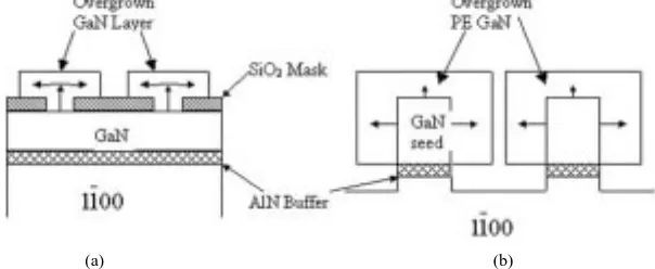
Fig. 1. Schematic of (a) LEO growth through a window in SiO and laterally over the mask. (b) PE growth from GaN seed laterally off the sidewalls and vertically off the stripe.
on the transport of the reactant gases to the surface and layer composition and uniformity are controlled by the reactor ge-ometry and flow conditions.
A complete range of solid solutions can be deposited from pure GaN to pure AlN at substrate temperatures exceeding 1000 C. By contrast, only 30% In can be incorporated (essentially “captured”) into an MOVPE-grown GaN-based alloy prior to the onset of phase separation [2], [3]. Increasing the growth rate and the use of a nitrogen diluent increases the concentration of InN incorporated into a film at a given tem-perature [4]–[6]. Growth temtem-peratures 800 C are normally used.
B. Recent Advances in the MOVPE of GaN and AlGaN
Growth of thin films of GaN and selected AlGaN alloys have cleared three major hurdles: 1) heteroepitaxy, i.e., the epi-taxial growth of a layer on a substrate or another layer having a different chemical composition and/or crystallography via the use of intermediate GaN, AlN or AlGaN buffer layers [7]–[9]; 2) control of donor (n-type) and acceptor (p-type) doping with Si and Mg, respectively; and 3) a marked reduction in the dislocation density. The high residual electron concentrations in the early samples of GaN were almost universally attributed to the donor character of nitrogen vacancies. However, first-principles calculations by Van de Walle [10] showed that the energy of formation of nitrogen vacancies is too high for their incorporation in GaN during growth, but oxygen and silicon readily form donors. This theory has received experimental support as a result of: 1) the decrease/increase in the carrier concentration/mobility of undoped GaN following the development of high-purity ammonia sources having 200 ppb H O levels and 2) the controlled increase in the n-type carrier concentration without compensation via the measured introduction of oxygen with a 33-MeV donor energy level into a GaN film in an extremely clean growth environment via molecular beam epitaxy (MBE) [11]. The results of additional MBE studies are presented below.
The aforementioned high intrinsic donor concentration was an impediment, but not the only problem, in the achievement of p-type conductivity. More recent research showed that a postgrowth exposure to an electron beam [12] or thermal annealing in nitrogen [13] was needed to activate and ionize acceptor dopants, e.g., Mg, to achieve p-type GaN grown via MOVPE. It was subsequently determined [14], [15] that the growth in the presence of hydrogen results in
the formation Mg–H complexes on the growing surface that become incorporated into the film. Heating dissociates these complexes, but the H does not evaporate. A third problem in p-type doping in MOVPE reactors is the “Mg memory” effect that leads to very broad doping profiles, making careful - junction placement difficult. Donor (Si) and acceptor (Mg) doping and corresponding electrical behavior have also been achieved in AlGaN alloys to maximum AlN concentrations of 58% and 13%, respectively [16].
Essentially, all films of III-Nitride materials are het-eroepitaxially grown on sapphire [ –Al O (0001)] or silicon carbide [SiC(0001)]. These substrates have lattice parameters and coefficients of thermal expansion that are, respectively, 16% and 39% (sapphire) and 3.5% and 3.2% (SiC), relative to GaN. The residual stresses caused by these mismatches are accommodated by the formation of misfit and threading dislocations, the latter of which occur throughout thin films in densities of 10 cm . Edge and mixed (screw/edge) dislocations in GaN: 1) are nonradiative recombination centers [17]; 2) act as conduits for charge transport, which results in high leakage currents and slow breakdown of rectifying contacts; and 3) reduce significantly the lifetime of laser diodes. By comparison, dislocation densities in “bulk” GaN single crystals and MOVPE films grown on them are reported to be 10 cm [18]. The latter also exhibit on-axis full-width at half-maximum (FWHM) values of X-ray diffraction rocking curves of 20 arcsec donor-bound exciton (D X) linewidth of 114 eV and an acceptor-bound exciton (A X) linewidth of 95 eV [18]. These values are an order of magnitude lower than the best MOVPE lateral epitaxial overgrowth (LEO) GaN on sapphire [19], [20]. Unfortunately, the limited availability and small size of these crystals have restricted their use.
Many research groups have shown that LEO can reduce the dislocation density in GaN films grown by MOVPE. Early reports of the achievement of material having a low density of dislocations via lateral overgrowth by Nam et
al. [21] and the success of Nakamura et al. [22] in the
(a)
(b)
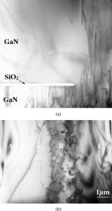
Fig. 2. (a) Cross-sectional TEM micrograph from a stripe along the [1120] direction. Two distinct regions of high-defect density above the window and of nearly defect-free GaN above the SiO are clearly visible. (b) Plan view TEM from a GaN stripe. Region A and C correspond to areas over the SiO and are nearly defect-free. Region B corresponds to the area over the window with a dislocation density of8 2 10 0 4 2 10 cm .
density of threading dislocations in the laterally overgrown layer is markedly reduced, as evidenced by the transmission electron microscopy (TEM) micrographs shown in Fig. 2 [23]. Pendeoepitaxy (PE) is another overgrowth technique in which GaN seed stripes are etched into the SiC substrate and GaN or AlGaN is regrown laterally and vertically off the stripe regions, as shown in Fig. 1(b). The dislocation density in the laterally grown sidewall regions is reduced by at least four orders of magnitude relative to the 10 cm density in the initial GaN seed layer, as shown in the Al Ga N film in Fig. 3 [24], [25].
PE incorporates mechanisms of growth exploited by con-ventional LEO processes with one main advantage, the elim-ination of the growth mask. Conventional LEO employs a SiO or SiN mask to stop the vertical propagations of de-fects into the overgrown material [21]. In PE, GaN selectively grows only off the etched GaN seed, as the substrate acts as a pseudomask and the overgrowth region coalesces and is sus-pended above the substrate [see Fig. 3(a)]. The elimination of a growth mask has three main advantages.
1) Crystallographic tilt in the overgrown material is sig-nificantly reduced. Tilt results in crystallographic
mis-Fig. 3. Composite of cross-sectional TEM micrographs of a PE Al Ga N film. Note the threading dislocations continue from the GaN stripes into the film.
registry and boundary formation at the region of coa-lescence [25], [26].
2) Diffusion of impurities from the mask into the over-growth material increases the background donor con-centration two orders of magnitude in LEO material [27]; carrier concentrations in PE remain below 1E17 cm .
3) AlGaN alloys nucleate on mask materials and PE pro-vides a means for growth of low-defect AlGaN films that cannot be accomplished with LEO [28].
Measurement of strain in GaN films grown via PE indi-cates that the overgrowth or wing material is crystallograph-ically relaxed. The presence of screw- and edge-type disloca-tions in the stripe and wing areas were determined via scans of the (0002) and ( ) X-ray reflections, as described in [29]. The FWHM values of the rocking curves in the on-axis (0002) reflection compare the concentration of screw-type dislocations while comparisons of off-axis ( ) FWHM values determine the relative density of edge-type disloca-tions. Reciprocal space maps of the uncoalesced PE material show a center peak produced by the seed material and two side peaks produced by the two wings when the beam direc-tion is perpendicular to the seed stripe direcdirec-tion. A reducdirec-tion in screw-type dislocations in the wings with respect to the stripes is indicated by a reduction in FWHM of the (0002) re-flections from 646 arcsec to 354 arcsec. The off-axis FWHM of the wing area was 126 arcsec compared to 296 arcsec for the stripe, indicating a reduction in the edge type dislocations as well.
with a FWHM value less than 300 eV (below the resolution of the equipment) and is comparable to homoepitaxy GaN grown on bulk GaN crystals [19]. PE growth of wings off the ( ) surface of a GaN stripe produces a material that is crystallographically relaxed, contains fewer defects com-pared to the stripe, and is atomically smooth on the ( ) surface [31].
Recently, considerable achievements in the homoepitaxial growth and doping of GaN thin films and microelectronic de-vice structures on MOVPE-derived GaN films via MBE have been reported. As such, this technique is becoming competi-tive with MOVPE in some areas for the growth of III-nitrides. The following section details the recent progress and scien-tific understanding in this arena.
II. PROGRESS IN THEMOLECULARBEAMEPITAXY OFGaN ANDITSALLOYS
The growth of thin films by MBE occurs via reactions be-tween thermal-energy molecular, atomic, or ionized beams of the constituent elements on a heated substrate in ultrahigh vacuum. The film composition depends on the relative arrival rates of the constituent elements that, in turn, depend on the evaporation rates or flow rates of the sources. The growth rate of the film is typically one monolayer per second. Mechan-ical shutters in front of the beam sources are used to interrupt the beam fluxes and, therefore, start and stop the deposition. Changes in composition can, thus, be abrupt on an atomic scale.
Homoepitaxial growth of GaN by MBE on 1–2- m-thick GaN “template” layers deposited via MOVPE on either sapphire or Si substrates has been investigated at the University of California at Santa Barbara (UCSB) [32] in collaboration with investigators at Infineon. The templates and the 0.2–0.5- m-thick MBE films have Ga polarity and threading dislocation densities in the mid-10 –10 cm range [33]. Growth diagrams have been instrumental in MBE growth [34], [35]. A regime within a diagram defines a set of growth conditions, i.e., group-III/group-V ratio versus substrate temperature that produces similar surface properties. Films grown under conditions that produce the same surface structure have been found to have similar properties [34], [35]. As such, these diagrams can be used to identify optimum growth regimes.
The characteristics of GaN surfaces have been studied by reflection high-energy electron diffraction (RHEED) surface reconstructions, atomic force microscopy (AFM), and scanning tunneling microscopy (STM) as a function of growth parameters. There seems to be a universal de-pendence of the surface morphology on the Ga/N ratio. Several groups [23], [36]–[39] have reported an abrupt transition in surface morphology between films grown under Ga-stable conditions (high Ga/N ratio) and those grown under N-stable conditions (low Ga/N ratios). Under N-stable conditions, films generally have spotty RHEED patterns and rough faceted morphologies. Ga-stable conditions (high Ga/N ratio) generally produce films having streaky RHEED patterns with smooth two-dimensional (2-D) growth morphologies. Ga-droplet formation has been found
(a)
(b)
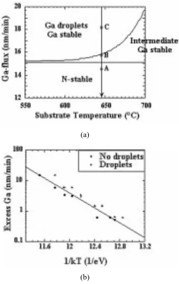
Fig. 4. (a) Surface structure diagram defining the Ga-flux conditions and substrate temperatures for the Ga droplet, intermediate, and N-stable growth regimes at a constant N flux of 15.2 nm/min. The closed circles, labeled A, B, and C, refer to the growth conditions of the samples shown in the AFM and TEM images. (b) Plot of excess Ga versus 1/kT, where the parameter excess Ga= F 0 F . (F is the Ga flux andF is the active nitrogen flux that gives rise to growth). The line was fit between the samples exhibiting droplets after growth and those that did not have droplets.
to accompany Ga-stable growth under conditions of high Ga/N ratios and low substrate temperatures [32], [37], [40].
The results of studies at UCSB [41] have defined three MBE growth regimes for GaN. The growth diagram shown in Fig. 4 depicts the Ga-flux conditions and substrate temper-atures that define these growth regimes at a constant N flux. Films grown with streaky RHEED patterns that exhibit Ga droplets characterize the “Ga-droplet” regime. These films were observed at low temperatures and high Ga fluxes. Films grown with streaky RHEED patterns that did not have Ga droplets were observed at high temperatures and interme-diate Ga fluxes and occurred in the “intermeinterme-diate” regime. The “N-stable” regime, characterized by films having spotty RHEED patterns, was observed at low Ga fluxes for all tem-peratures.
(a)
(b)
(c)
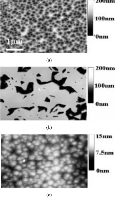
Fig. 5. AFM images of GaN samples grown within the (a) N-stable regime (Ga flux= 14.5 nm/min), (b) intermediate regime (Ga flux= 15.8 nm/min), and (c) Ga droplet regime (Ga flux = 18.2 nm/min).
boundary corresponds to the aforementioned transition between spotty and streaky RHEED patterns. This boundary is constant for all temperatures within the diagram because no temperature dependence was observed in the growth rate of Ga-stable films or N-stable films to at least 700 C.
Growing films under various fluxes and temperatures and subsequently observing whether droplets formed during growth determined the boundary between the intermediate growth regime and the Ga-droplet growth regime. The curve shown in Fig. 4(b) was fit between the samples exhibiting droplets and those that did not. It had an Arrhenius depen-dence with activation energy of 2.832 eV, which corresponds to the activation energy for desorption of Ga from liquid Ga. Films grown within the N-stable regime have a very rough crater-like morphology, as shown in Fig. 5(a). The surface of the films grown within the intermediate Ga-stable regime [see Fig. 5(b)] have large areas of uniform flat surface between pits with irregular faceted edges. The film grown within the Ga droplet regime [see Fig. 5(c)] shows no pit fea-tures and has a uniform atomically flat surface. The mottled appearance of the surfaces grown in the Ga-stable regime is caused by spiral growth about threading dislocations with mixed character. TEM studies on the last samples revealed that the pit features shown in Fig. 5(b) were associated with inclined facets that form at threading dislocations. These facets typically are or planes and are the
Fig. 6. Growth diagram defining the Ga-flux conditions and substrate temperatures for the Ga droplet, intermediate, and N-stable growth regimes at a constant N flux of 2.8 nm/min. Circles define the conditions used for transport studies for n-type GaN.
Table 1
RT Mobilities and Carrier Concentrations in Samples Grown Under the Conditions Signified by the Circles Shown in Fig. 6
MBE equivalent to the common facets observed in MOVPE GaN films.
As noted above, the commonly introduced acceptor is Mg, which has a thermal activation energy of 120–200 MeV. Very sharp Mg doping profiles, both at the upper and lower interfaces for buried finite-thickness radio-frequency (RF) plasma MBE-grown layers, and hole mobilities and carrier concentrations comparable to the state-of-the-art MOVPE material have been reported [44] without the necessity for thermal annealing or the presence of the aforementioned “Mg memory” effect that is common in MOVPE reactors. The highest hole mobilities and the best surface morphologies for MBE-derived GaN have been observed at the crossover from the intermediate Ga-rich regime to the Ga-droplet regime in the growth diagram [45].
RF-plasma MBE has also been very successfully used for the development of high mobility 2-D electron gases (2DEGs) in the AlGaN/GaN system. For growth on Ga polar templates, a fixed positive sheet charge exists at the AlGaN/GaN interface due to the discontinuity in the total polarization between AlGaN and GaN. When the AlGaN cap layer exceeds a minimum thickness, a 2DEG forms at the interface. Contrary to results in MOVPE AlGaN/GaN structures, the 2DEG mobility for MBE AlGaN/GaN struc-tures decreases with increasing sheet carrier concentration [46]. This indicates that the dominant scattering mechanism in MBE structures is either alloy scattering or interface roughness and not ionized impurity scattering. Thus, the highest mobilities in MBE structures have been realized at low Al concentrations and now exceed 60 000 cm /V s at 4 K [47], a value about twice as large as reported in the best MOVPE AlGaN/GaN structures. This overall improvement in mobility is likely due to the reduction in unintentional impurity incorporation in the MBE environment. Similar to the results for n-GaN and p-GaN, 2DEGs with superior elec-trical properties are realized when the growth is conducted at the cross over from the intermediate Ga-rich regime to the Ga-droplet regime [48].
Thin films produced by any technique must be accompa-nied by characterization to provide both basic scientific under-standing of the materials and to inform the grower regarding changes that must be made in the process route to achieve im-proved properties. Microstructural and electrical properties of the MOVPE and MBE films were described in the foregoing sections. However, these must be accompanied by optical and magnetic resonance studies to obtain important information regarding the vibrational characteristics; the presence, iden-tity, and properties of intentionally and unintentionally intro-duced impurities that may or may not be electrically active; and the chemical identity and density of point defects and their magnetic properties. The following two sections address the capabilities and recent achievements in optical and magnetic resonance characterization of GaN films.
III. OPTICALSTUDIES OFUNDOPED ANDDOPEDGaN SEMICONDUCTORS
A. Overview of Selected Techniques
PL is a sensitive and nondestructive technique for the detection and identification of impurities and other defects
in semiconductors. Electrons and holes optically excited across the forbidden energy gap usually become localized or bound at an impurity or defect before recombining. The identity of the localized center to which they are bound can often be determined on the basis of the binding energies in-ferred from the spectral positions or from thermal quenching studies. Qualitative information regarding the structural and microstructural characteristics can be accessed from the efficiency and line widths of near band edge PL spectra. A broad scope of phenomena such as excitation, recombi-nation mechanisms, structural defects, and impurities can be investigated. In general, a number of defects present simultaneously in the material can compete at different rates for the photo-excited carriers resulting in radiative or nonradiative recombination processes. Therefore, PL is not adequate to provide the concentration of defects.
Raman scattering (RS) allows one to study vibrational phenomena in solids. Inelastic light scattering in crystals is susceptible to selection rules originating from momentum conservation [49]. Therefore, RS can be used to assess both the structure and microstructure of bulk and epitaxial layers. Fourier transform infrared (FTIR) absorption is a non-destructive technique to quantify neutral electrically active donors and acceptors. Photons with energies equal to the energy necessary to promote electrons or holes from the ground state to the excited states can be absorbed yielding an intrinsic optical signature of the donors and acceptors. Providing that the excited states are bound to the band by an energy that depends weakly on the nature of the donor or acceptor, the ground-to-excited state transitions of different donors/acceptors are relatively displaced by approximately the difference between their ground state binding energies.
B. Recent Progress in the Optical Characterization of GaN Thin Films
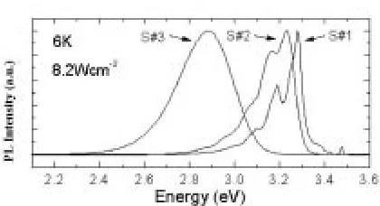
Fig. 7. Normalized low-temperature PL spectra of three GaN : Mg HE films deposited by MOCVD on a-face sapphire. Note the line shape change and the red-shift of the peak position with increasing Mg concentration, from2:5 2 10 to 7 2 10 cm . These samples have been postgrowth thermal annealed at 950 C. Spectra are corrected for instrumental response.
processes associated with the annihilation of free-excitons (FEs) and excitons bound to a neutral shallow donor (D X) [54], [55]. Typical values of the D X full-width-at-half-max-imum (FWHM) linewidth at 6 K are 3 MeV and for FE at 300 K 33 MeV for good UID heteroepitaxial (HE) layers [54]. The RS spectra of such materials showed all the six allowed modes with small FWHM values, which are con-sistent with wurtzite films without high values of residual stress. The PL spectrum of a typical Si-doped film consists of a weak 2.25-eV band and an intense edge emission assigned to a recombination process associated with X–Si (i.e., exci-tons bound to shallow Si donors). Films deposited with these optimized growth conditions have been successfully used for fabrication of high-yield field-effect transistors [56].
As noted above, Mg has a binding energy of 200 MeV in GaN. As such, only about 1% of the atoms are electrically active at RT. Therefore, a higher doping level is required to provide the RT hole concentrations necessary for device fab-rication. However, a deep compensating donor is apparently introduced with increasing activated Mg concentration. The 6-K PL spectra of three GaN films doped with different con-centrations of Mg are shown in Fig. 7. Note the shift between curves (a) and (b) and between (b) and (c). The first shift orig-inates from potential fluctuations induced by charged donor and acceptor centers and the latter is assigned to a recombi-nation process involving a deep donor and the Mg acceptor [57], [58].
C. Optical Properties of the State-of-the-Art GaN Films
The structural and optical properties of homoepitaxial GaN films can be used as a benchmark to which HE GaN films may be compared [59]. To reduce the usual high density of structural defects in HE layers, patterned HE GaN films have been developed for selective deposition of low defect density GaN overlayers, as described in Section I. TEM and X-ray diffraction studies of these LEO layers show that the LEO region contains a lower density of dislocations [60]. However, the regions of coalescence of the lateral growth fronts are characterized by a high concentration of extended defects resulting from the tilting and resultant crystallographic misalignment described in Section I. This problem is considerably reduced in the
Fig. 8. First-order polarized RS spectra of a170-m-thick freestanding GaN template. These spectra are consistent with high crystalline quality relaxed material.
PE films also described in Section I. Another approach to control the propagation of dislocations in HE layers has been the growth of multiple GaN layers with intermediary AlN low-temperature NLs. A considerable increase in carrier mobility has been reported using this approach that may be associated with the reduction in the density of the threading screw dislocations; however, incorporation of a large concentration of donors has been observed in these UID highly strained layers [61].
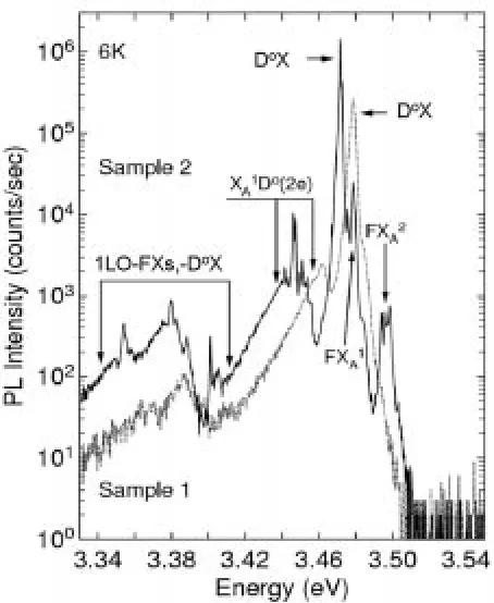
Freestanding films (FSs) of GaN grown via hydride vapor phase epitaxy (HVPE) with a thickness of 400 m have been removed from sapphire substrates by laser-assisted liftoff, mechanically polished and reactive-ion etched to yield 200- m-thick flat and smooth templates that can be used for homoepitaxial growth [62]. These substrates possess a low background donor concentration (
Fig. 9. High-resolution band edge PL spectra of two representative HVPE samples. Sample 1 is still on the sapphire substrate and sample 2 was removed using a laser liftoff technique. Presence of a variety of sharp excitonic lines in this spectral region confirms the single crystalline nature and the low densities of dislocations and other defects in both samples.
2.69 MeV; for sample 2, it is only 370 eV [64]. A 6.2-MeV shift to higher energy resulting from the compressive strain has been measured for sample 1. The results of detailed FTIR and secondary ion mass spectrometry (SIMS) studies conducted on these samples have revealed two pervasive donors. The more shallow and the deeper donors are Si and O, with binding energies of 30.19 0.1 MeV and 33.21 0.1 MeV, respectively [65].
IV. CHARACTERIZATION OFDEFECTS INGaNANDRELATED ALLOYS BYMAGNETICRESONANCETECHNIQUES
A. Overview of the Techniques
The interaction of the electronic spin and an applied mag-netic field splits the ground and excited states associated with point defects, e.g., dopants, transition metals, vacancies, in-terstitial atoms, and antisites, into two or more levels. In principle, transitions between these levels can be detected by spin resonance techniques such as electron paramagnetic resonance (EPR) and optically detected magnetic resonance (ODMR). In addition to giving important information such as chemical identification of the defect through Zeeman split-tings ( factors) and resolved hyperfine (HF) structure, EPR can provide a quantitative measure of the defect densities in the material. Though not quantitative, ODMR combines the attributes of EPR with the sensitivity and selectivity of PL. In particular, this technique gives information on the magnetic properties of the optically excited donor and acceptor states,
e.g., that participate directly (or sometimes indirectly) in ra-diative recombination processes [66].
B. Magnetic Resonance Research on III-Nitrides
Very little magnetic resonance work on GaN and related materials was reported prior to 1990. One example is the nuclear magnetic resonance (NMR) experiments performed on GaN bulk powders that gave the magnitude of the electric field gradients at the host lattice sites [67]. In parallel with the dramatic advances in materials growth and device development, an international effort has been ongoing since that time to obtain a better understanding of the properties of residual defects and dopants in GaN through magnetic res-onance techniques. Most of the EPR and ODMR have been performed on as-grown (n-type and highly resistive) and Si-, Mg-, or Be-doped wurtzite (hexagonal) GaN HE layers [68]–[72] with little work reported for zincblende (cubic) GaN [73]. Some research (mainly EPR) has been conducted on n-type (as-grown or Si-doped) Al Ga N HE layers [74], [75] and, surprisingly, little magnetic resonance has been reported for InGaN epitaxial layers with the exception of In Ga N-based light-emitting diode structures [76], [77].
A variety of defects of donor and acceptor character have been revealed by EPR, ODMR, and related techniques in these GaN-based materials and device structures. However, their microscopic identities have been a challenge based on the absence of resolved HF structure in most cases. Some exceptions where defect identification has been possible in-clude residual transition metals in GaN such as Fe, Ni, Mn, and Cu as well as Ga interstitial-related defects observed re-cently by ODMR on IR emission from electron-irradiated GaN [78]. Examples of magnetic resonance characterization of defects in GaN and related alloys are given below.
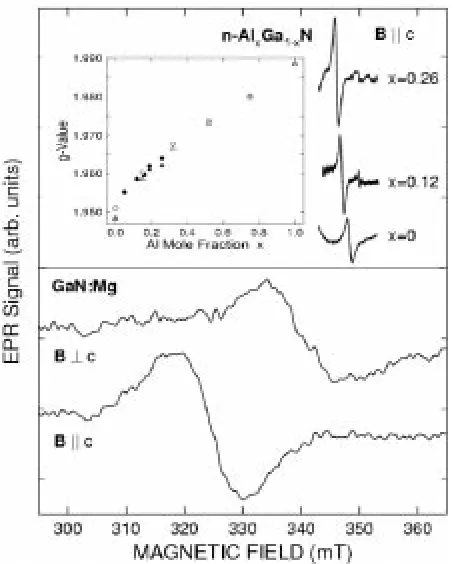
The EPR spectra obtained at 9.5 GHz for as-grown (n-type) GaN and Al Ga N ( 0.12 and 0.26) HE layers grown on 6H–SiC(0001) by MOVPE are shown in the top half of Fig. 10. A single line with axial symmetry
about the axis with and is
found from the GaN film and has been firmly established as a “fingerprint” for shallow donors/conduction electrons [68]. The small shift (i.e., 0.05) from the free-electron value of 2.0023 is in good agreement with that predicted from multiband k p effective-mass (EM) theory [68], [75]. It is generally agreed that likely candidates for residual shallow donors in these materials are Si and O. Unfor-tunately, in contrast to the case of Si, where the EPR is much sharper and different donors could be distinguished by their values [79], it is not expected that a difference in values can be detected for shallow donors with similar binding energies in GaN. For the EPR of shallow donors in Al Ga N, the monotonic increase of the values (see inset in Fig. 10) toward the value of two with increasing Al mole fraction reflects the decrease in spin-orbit splittings of the valence and upper conduction bands and the increase of the interband energies [74], [75].
Fig. 10. Top: EPR spectra found at 9.5 GHz for as-grown (n-type) GaN and Al Ga N epitaxial layers. Also shown is a plot of the donorg values versus Al mole fraction. Closed symbols are from [74], open symbols are from [75]. Circles:g factors with B
k c; triangles: g factors with B ? c. Bottom: EPR spectra for a
Mg-doped (p-type) GaN film.
the need for contacts or the high temperatures required (due to the large ionization energy of 200 MeV) for Hall effect measurements. For example, representative spectra obtained for a Mg-doped GaN sample grown on sapphire by MOVPE with a RT free hole carrier density of 1.7 10 cm are shown in the bottom half of Fig. 10. A single
resonance is found with and and a
spin density of 4 10 cm . This feature is assigned to shallow Mg acceptors based on the similarity of the EPR spin density with the concentration of electronically active Mg acceptors determined by temperature-dependent Hall effect and the total Mg level as revealed by SIMS. In addition, similar magnetic resonance parameters have been found from ODMR studies of shallow Mg acceptors [80] involved in shallow donor–shallow acceptor recombination (ZPL at 3.27 eV) from Mg-doped GaN.
The PL most studied in GaN by ODMR during the last decade is the ubiquitous 2.2-eV emission band [69]–[71]. The spectra obtained using this technique at 24 GHz from n-type (as-grown or Si-doped) GaN epitaxial layers grown by MOVPE, HVPE, and MBE are shown in Fig. 11. The spectra are very similar in spite of the radically different growth
tech-niques. The sharp line with and is
as-signed to (EM) shallow donors based on the EPR work [68]. Most groups associate the broader feature with
and to deep defects. This center was first as-signed to deep donors [69] from the small negative g-shift
rel-Fig. 11. ODMR obtained at 24 GHz on the 2.2-eV “yellow” PL band from n-type GaN grown by CVD, HVPE, and MBE. Inset: ODENDOR spectra found on the shallow donor resonance from an as-grown (highly resistive) GaN sample [83]. Features are attributed to Ga host lattice nuclei that sense the WZ crystal field and local strains through the nuclear quadrupole interaction. Similar ODENDOR has been reported on theg = 1:992 deep defect ODMR [71].
ative to the free-electron -value of 2.0023. However, based on the observation of similar g-shifts for Mg-shallow ac-ceptors in subsequent EPR and ODMR studies (e.g.,
), the donor or acceptor character of this deep center is an open question from a magnetic resonance viewpoint. It has been suggested from the results of other techniques [81] and theory [82] that deep levels, associated with Ga vacan-cies or their complexes, are involved in 2.2-eV PL. More sophisticated magnetic resonance techniques have been ap-plied to determine the origins of both this deep defect and residual shallow donors in GaN. In particular, several groups have performed optically detected electron-nuclear double-resonance experiments [71], [83], [84] on the 2.2-eV band, but evidence has only been found for NMR associated with
Ga lattice nuclei (see inset in Fig. 11).
V. SUMMARY
HE growth of (Al, In, Ga)N compounds and alloys at high rates, excellent compositional control, and uniformity over large areas, low background carrier concentrations, and donor (Si) and acceptor (Mg) doping have been ac-complished via MOVPE on sapphire, SiC, and bulk GaN substrates. However, the Mg memory effect in the system is a significant problem. LEO and/or PE produce GaN and AlGaN continuous layers with a reduced density of dislo-cations, a reduced strain, and strong sharp optical emission; however, tilting and coalescence boundaries are produced by the laterally growing material.
Very high electron mobilities in both n-type GaN and in 2DEGs at the AlGaN/GaN interface have been realized by RF plasma-assisted MBE of these materials on thin-film GaN substrates at the crossover from the intermediate growth regime to the droplet regime in the growth diagram. Transport properties and the sharpness of the Mg doping profiles in p-type GaN exceed the best achieved via MOVPE. In addition, there is no Mg memory effect. Heterogeneous growth, substrate temperature uniformity, and flux control are the significant challenges for MBE.
PL results of MOVPE-derived UID HE GaN films showed sharp lines near 3.478 eV due to recombination processes associated with the annihilation of FEs and excitons bound to a neutral shallow donor (D X). For good HE films, FWHM linewidths for D X at 6 K are 3 MeV and for FE at 300 K are 33 MeV. The RS spectra of such materials showed all the six allowed modes with small FWHM values. The PL spectrum of a typical Si-doped film consists of a weak 2.25-eV band and an intense edge emission assigned to recombination process associated with X–Si . A deep compensating donor is introduced with increasing concentration of the Mg acceptor. The spectrum of HVPE-derived FS GaN templates shows, within the 3.46–3.52-eV region, emission lines assigned to the excited state of the FE A (FX ) and the dominant D X. At 3.45 eV, the two-electron satellite spectrum resulting from the recombination processes in which the D is left in an excited state after the excitons annihilation is observed. FTIR and SIMS studies conducted on the FS samples have revealed the pervasive donors to be Si and O.
The EPR for n-type GaN and Al Ga N HE layers shows single lines with axial symmetry about the axis with and between 1.94 and 1.99. This has been established as a “fingerprint” for shallow donors/conduction electrons. EPR for p-type GaN samples reveals a single resonance
feature with and , which has been
assigned to shallow Mg acceptors. ODMR of the 2.2-eV emission band from n-type GaN epitaxial layers grown by MOVPE, HVPE, and MBE are similar. The sharp line
with and has been assigned to
shallow donors. Most groups associate the broader feature
with and to deep defects whose
electronic character remains controversial. ODMR measure-ments of electron-irradiated GaN have identified the Ga based on well-resolved HF structure.
REFERENCES
[1] S. Jingxi, J. M. Redwing, and T. F. Kuech, “Model development of GaN MOVPE growth chemistry for reactor design,” J. Electron.
Mater., vol. 29, pp. 2–9, Jan. 2000.
[2] N. Elmasry, E. Piner, S. Liu, and S. Bedair, “Phase separation in InGaN grown by metal–organic chemical vapor deposition,” Appl.
Phys. Lett., vol. 72, pp. 40–42, Jan. 1998.
[3] M. McCluskey, L. Romano, B. Krusor, D. Bour, N. Johnson, and N. Brennan, “Phase separation in InGaN/GaN multiple quantum wells,”
Appl. Phys. Lett., vol. 72, pp. 1730–1732, Apr. 1998.
[4] S. M. Bedair, F. G. McIntosh, J. C. Roberts, E. L. Piner, K. S. Boutros, and N. A. El-Masry, “Growth and characterization of in-based nitride compounds,” J. Cryst. Growth, vol. 178, pp. 32–44, June 1997. [5] S. Keller, B. P. Keller, D. Kapolnek, U. K. Mishra, S. P. DenBaars, I.
K. Shmagin, R. M. Kolbas, and S. Krishnankutty, “Growth of bulk InGaN films and quantum wells by atmospheric pressure metal–or-ganic chemical vapor deposition,” J. Cryst. Growth, vol. 170, pp. 349–352, Jan. 1997.
[6] S. Keller, B. P. Keller, D. Kapolneck, A. C. Abare, H. Masui, L. A. Coldren, U. K. Mishra, and S. P. DenBaars, “Growth and character-ization of bulk InGaN films and quantum wells,” Appl. Phys. Lett., vol. 68, pp. 3147–3149, May 1996.
[7] S. Nakamura, “GaN growth using GaN buffer layer,” Jpn. J. Appl.
Phys., vol. 30, pp. L1705–L1707, Oct. 1991.
[8] H. Amano, N. Sawaki, I. Akasaki, and Y. Toyoda, “Metal–organic vapor phase epitaxial growth of a high quality GaN film using an AlN buffer layer,” Appl. Phys. Lett., vol. 48, pp. 353–355, Feb. 1986. [9] W. Weeks, M. D. Bremser, K. Ailey, E. Carlson, W. Perry, and R. F. Davis, “GaN thin films deposited via organometallic vapor phase epi-taxy on 6H–SiC(0001) using high-temperature monocrystalline AlN buffer layers,” Appl. Phys. Lett., vol. 67, pp. 401–403, May 1995. [10] C. Van de Walle, C. Stampfl, and J. Neugebauer, “Theory of doping
and defects in III–V nitrides,” J. Cryst. Growth, vol. 189/190, pp. 505–510, June 1998.
[11] A. J. Ptak, L. J. Holbert, C. H. Swartz, L. Wang, N. C. Giles, T. H. Myers, G. C. B. Braga, J. A. Freitas, D. D. Koleske, R. L. Henry, A. E. Wickenden, C. Tian, A. Hockett, S. Mithra, and P. Van Lierde, pre-sented at the 43rd Electronic Materials Conf., Notre Dame, IN, 2001. [12] H. Amano, M. Kito, K. Hiramatsu, and I. Akasaki, “P-type conduc-tion in Mg-doped GaN treated with low-energy electron beam irradi-ation (LEEBI),” Jpn. J. Appl. Phys., pt. 2, vol. 28, pp. L2112–L2114, Dec. 1989.
[13] S. Nakamura, “Thermal annealing effects on P-type Mg-doped GaN films,” Jpn. J. Appl. Phys., vol. 31, pp. L139–L142, Feb. 1992. [14] W. Gotz, N. M. Johnson, J. Walker, D. P. Bour, and R. A. Street,
“Activation of acceptors in Mg-doped GaN grown by netalorganic chemical vapor deposition,” Appl. Phys. Lett., vol. 68, pp. 667–669, Jan. 1996.
[15] M. Miyachi, T. Tanaka, Y. Kiumur, and H. Ota, “The activation of Mg in GaN by annealing with minority-carrier injection,” Appl.
Phys. Lett., vol. 72, pp. 1101–1103, Mar. 1998.
[16] M. D. Bremser, W. G. Perry, O. H. Nam, D. P. Griffis, R. Loesing, D. A. Ricks, and R. F. Davis, “Acceptor and donor doping of AlGaN thin film alloys grown on 6H–SiC(0001) substrates via metal–or-ganic vapor phase epitaxy,” J. Electron. Mater., vol. 27, pp. 229–232, Apr. 1998.
[17] T. Sugahara, H. Sato, M. Hao, Y. Naoi, S. Kurai, S. Tottori, K. Ya-mashita, K. Nishino, L. T. Romano, and S. Sakai, “Direct evidence that dislocations are nonradiative recombination centers in GaN,”
Jpn. J. Appl. Phys., vol. 37, pp. L398–L400, Apr. 1998.
[18] M. Leszczynski, B. Beaumont, E. Frayssinet, W. Knap, P. Prystawko, T. Suski, I. Grzegory, and S. Porowski, “GaN homoepitaxial layers grown by metal–organic chemical vapor deposition,” Appl. Phys.
Lett., vol. 75, pp. 1276–1278, Aug. 1999.
[19] C. Kirchner, V. Schwegler, F. Eberhard, M. Kamp, K. J. Ebeling, K. Kornitzer, T. Ebner, K. Thonke, R. Sauer, P. Prystawko, M. Leszczynski, I. Grzegory, and S. Porowski, “Homoepitaxial growth of GaN by metal–organic vapor phase epitaxy: A benchmark for GaN technology,” Appl. Phys. Lett., vol. 75, pp. 1098–1100, Aug. 1999. [20] B. Beaumont, M. Vaille, G. Nataf, A. Bouille, J. C. Guillaume, P.
Vennegues, S. Haffouz, and P. Gibart, “Mg-enhanced lateral over-growth of GaN on patterned GaN/sapphire substrate by selective metal organic vapor phase epitaxy,” MRS Internet J. Nitride
Semi-cond. Res., vol. 3, p. 20, 1998.
[22] S. Nakamura, “InGaN/GaN/AlGaN-based laser diodes with an esti-mated lifetime of longer than 10 000 hours,” MRS Bullet., vol. 23, pp. 37–43, May 1998.
[23] O. H. Nam, T. S. Zheleva, M. D. Bremser, and R. F. Davis, “Lateral epitaxial overgrowth of GaN films on SiO areas via metal–organic vapor phase epitaxy,” J. Electron. Mater., vol. 27, pp. 233–237, Mar. 1998.
[24] T. Zheleva, S. Smith, D. Thomson, and K. Linthicum, “Pendeo-epi-taxy—A new approach for lateral growth of gallium nitride films,”
J. Electron. Mater., vol. 28, pp. L5–L8, Apr. 1999.
[25] R. F. Davis, T. Gehrke, K. J. Linthicum, T. S. Zheleva, E. A. Preble, P. Rajagopal, C. A. Zorman, and M. Mehregany, “Pendeo-epitaxial growth of thin films of gallium nitride and related materials and their characterization,” J. Cryst. Growth, vol. 225, pp. 134–140, May 2001.
[26] T. Gehrke, K. J. Linthicum, E. Preble, P. Rajagopal, C. Ronning, C. Zorman, M. Mehregany, and R. F. Davis, “Pendeo-epitaxial growth of gallium nitride on silicon substrates,” J. Electron. Mater., vol. 29, pp. 306–310, Mar. 2000.
[27] F. Bertram, T. Riemann, J. Christen, A. Kaschner, A. Hoffmann, C. Thomsen, K. Hiramatsu, T. Shibata, and N. Sawaki, “Strain relaxation and strong impurity incorporation in epitaxial laterally overgrown GaN: Direct imaging of different growth domains by cathodoluminescence microscopy and micro-raman spectroscopy,”
Appl. Phys. Lett., vol. 74, pp. 359–361, Jan. 1999.
[28] T. Gehrke, K. J. Linthicum, D. B. Thomson, P. Rajagopal, A. D. Batchelor, and R. F. Davis, “Pendeo-epitaxy of gallium nitride and aluminum nitride films and heterostructures on silicon carbide sub-strate,” MRS Internet J. Semicond. Res., vol. 4S1, 1999.
[29] H. Heinke, V. Kirchner, S. Einfeldt, and D. Hommel, “Analysis of the defect structure of epitaxial GaN,” Phys. Stat. Sol. (a), vol. 176, pp. 391–395, Nov. 1999.
[30] C. Kisielowski, J. Kruger, S. Runimov, T. Suski, J. W. Ager, III., E. Jones, Z. Liliental-Weber, M. Ruben, E. R. Weber, M. D. Bremser, and R. F. Davis, “Strain-related phenomena in GaN thin films,” Phys.
Rev. B, vol. 54, pp. 17 745–17 753, Dec. 1996.
[31] A. M. Roskowski, P. Q. Miraglia, E. A. Preble, S. Einfeldt, T. Stiles, R. F. Davis, J. Schuck, R. Grober, and U. Schwarz, “Strain and dislo-cation reduction in maskless pendeo-epitaxy GaN thin films,” Phys.
Stat. Sol. (a), vol. 188, no. 2, pp. 729–732, Nov. 2001.
[32] E. J. Tarsa, B. Heying, X. H. Wu, P. Fini, S. P. DenBaars, and J. S. Speck, “Homoepitaxial growth of GaN under Ga-stable and N-stable conditions by plasma-assisted molecular beam epitaxy,” J.
Appl. Phys., vol. 82, no. 11, pp. 5472–5479, Dec. 1997.
[33] X. H. Wu, L. M. Brown, D. Kapolnek, S. Keller, B. Keller, S. P. DenBaars, and J. S. Speck, “Defect structure of metal-organic chem-ical vapor deposition-grown epitaxial (0001) GaN/Al O ,” J. Appl.
Phys., vol. 80, no. 6, pp. 3228–3237, Sept. 1996.
[34] S. M. Newstead, R. A. A. Kubiak, and E.H.C. Parker, “On the prac-tical applications of MBE surface phase diagrams,” J. Cryst. Growth, vol. 81, no. 1–4, pp. 49–54, Feb. 1987.
[35] S. Y. Karpov, Y. V. Kovalchuk, V. E. Myachin, and Y. V. Pogorel-skii, “Instability of III–V compound surfaces due to liquid phase formation,” J. Cryst. Growth, vol. 129, no. 3–4, pp. 563–570, Apr. 1993.
[36] H. Okumura, K. Balakrishnan, H. Hamaguchi, T. Koizumi, S. Chichibu, H. Nakanishi, T. Nagatomo, and S. Yoshida, “Analysis of MBE growth mode for GaN epilayers by RHEED,” J. Cryst.
Growth, vol. 189/190, pp. 364–369, June 1998.
[37] R. Held, D. E. Crawford, A. M. Johnston, A. M. Dabiran, and P. I. Cohen, “In situ control of GaN growth by molecular beam epitaxy,”
J. Electron. Mater., vol. 26, no. 3, pp. 272–280, Mar. 1997.
[38] R. Held, G. Nowak, B. E. Ishaug, S. M. Seutter, A. Parkhomovsky, A. M. Dabiran, P. I. Cohen, I. Grzegory, and S. Porowski, “Structure and composition of GaN(0001) A and B surfaces,” J. Appl. Phys., vol. 85, no. 11, pp. 7697–7704, June 1999.
[39] H. Riechert, R. Averbeck, A. Graber, M. Schienle, U. Strauss, and H. Tews, “Optimized structural properties of wurtzite GaN on SiC(0001) grown by molecular beam epitaxy,” Proc. Mater. Res.
Soc. Symp., vol. 449, pp. 149–159, 1997.
[40] P. Hacke, G. Feuillet, H. Okumura, and S. Yoshida, “Monitoring sur-face stoichiometry with the (22 2) reconstruction during grwth of hexagonal phase GaN by molecular beam epitaxy,” Appl. Phys. Lett., vol. 69, no. 17, pp. 2507–2509, Oct. 1996.
[41] B. Heying, R. Averbeck, L. F. Chen, E. Haus, H. Riechert, and J. S. Speck, “Dislocation mediated surface morphology of GaN,” J. Appl.
Phys., vol. 88, no. 4, pp. 1855–1860, Aug. 2000.
[42] B. Heying, I. Smorchkova, C. Poblenz, C. Elsass, P. Fini, S. Den Baars, U. Mishra, and J. S. Speck, “Optimization of the surface morphologies and electron mobilities in GaN grown by plasma-as-sisted molecular beam epitaxy,” Appl. Phys. Lett., vol. 77, no. 18, pp. 2885–2887, Oct. 2000.
[43] B. Heying, T. Myers, and J. S. Speck, unpublished data.
[44] I. P. Smorchkova, E. Haus, B. Heying, P. Kozodoy, P. Fini, J. P. Ib-betson, S. Keller, S. P. DenBaars, J. S. Speck, and U. K. Mishra, “Mg doping of GaN layers grown by plasma-assisted molecular-beam epitaxy,” Appl. Phys. Lett., vol. 76, no. 6, pp. 718–720, Feb. 2000. [45] E. Haus, Y. Smorchkova, B. Heying, U. K. Mishra, S. P. DenBaars,
and J. S. Speck, unpublished data.
[46] I. P. Smorchkova, C. R. Elsass, J. P. Ibbetson, R. Vetury, B. Heying, P. Fini, E. Haus, S. P. DenBaars, J. S. Speck, and U. K. Mishra, “Po-larization-induced charge and electron mobility in AlGaN/GaN het-erostructures grown by plasma-assisted molecular-beam epitaxy,” J.
Appl. Phys., vol. 86, no. 8, pp. 4520–4526, Oct. 1999.
[47] C. R. Elsass, I. P. Smorchkova, B. Heying, E. Haus, C. Poblenz, P. Fini, K. Maranowski, P. M. Petroff, S. P. DenBaars, U. K. Mishra, J. S. Speck, A. Saxler, S. Elhamri, and W. C. Mitchel, “Effects of growth conditions on the incorporation of oxygen in AlGaN layers grown by plasma assisted molecular beam epitaxy,” Jpn. J. Appl.
Phys., vol. 39, no. 10B, pp. L1023–L1025, Oct. 2000.
[48] C. R. Elsass, C. Poblenz, B. Heying, P. Fini, P. M. Petroff, S. P. Den-Baars, U. K. Mishra, and J. S. Speck, “Influence of Ga flux on the growth and electron transport properties of AlGaN/GaN heterostruc-tures grown by plasma-assisted molecular beam epitaxy,” J. Cryst.
Growth, vol. 233, no. 4, pp. 709–716, Dec. 2001.
[49] M. Cardona, “Light scattering in solids,” in Topics in Applied
Physics Springer-Verlag, Germany, 1983, vol. 8.
[50] R. Dingle, D. D. Sell, S. E. Stokowski, and M. Ilegems, “Absorption, reflectance, and luminescence of GaN epitaxial layers,” Phys. Rev.
B, vol. 4, pp. 1211–1218, Aug. 1971.
[51] S. Yoshida, S. Misawa, and S. Gonda, “Improvements on the elec-trical and luminescence properties of reactive molecular beam epi-taxially grown films by using AlN-coated sapphire substrates,” Appl.
Phys. Lett., vol. 42, pp. 427–430, Mar. 1983.
[52] H. Amano, N. Sawaki, I. Akasaki, and T. Toyoda, “Metal–organic vapor phase epitaxial growth of a high quality GaN film using an AlN buffer layer,” Appl. Phys. Lett., vol. 48, pp. 353–355, Feb. 1986. [53] A. E. Wickenden, L. B. Rowland, K. Doverspike, D. K. Gaskill, J. A. Freitas, Jr., D. S. Simons, and P. H. Chi, “Doping of galliun nitride using disilane,” J. Electron. Mater., vol. 24, pp. 1547–1550, Nov. 1995.
[54] J. A. Freitas, Jr., K. Doverspike, and A. E. Wickenden, “Excitonic recombination processes in doped and undoped wurtzite GaN films deposited on sapphire substrates,” Proc. Mater. Res. Soc. Symp., vol. 395, pp. 485–490, 1996.
[55] W. Shan, T. J. Schmidt, X. H. Yang, S. J. Huang, J. J. Song, and B. Goldenberg, “Temperature dependence of interband transitions in GaN grown by metal–organic chemical vapor deposition,” Appl.
Phys. Lett., vol. 66, pp. 985–987, Feb. 1995.
[56] S. C. Binari, W. Kruppa, H. B. Dietrich, G. Kelner, A. E. Wickenden, and J. A. Freitas, Jr., “Fabrication and characterization of GaN FETs,” Solid-State Electron., vol. 41, pp. 1549–1554, Oct. 1997. [57] M. A. Reshchikov, G.-C. Yi, and B. W. Wessels, “Behavior of
2.8-and 3.2-eV photoluminescence b2.8-ands in Mg-doped GaN at different temperatures and excitation densities,” Phys. Rev. B, vol. 59, pp. 13 176–13183, May 1999.
[58] H. Teisseyre, T. Suski, P. Perlin, I. Grzegory, M. Leszczynski, M. Bockowski, S. Porowski, J. A. Freitas, Jr., R. L. Henry, A. E. Wickenden, and D. D. Koleske, “Different character of the donor-acceptor pair-related 3.27-eV band and blue photolumines-cence in Mg-doped GaN. Hydrostatic pressure studies,” Phys. Rev.
B, vol. 62, pp. 10 151–10 157, Oct. 2000.
[59] K. Kornitzer, T. Ebner, K. Thonke, R. Sauer, C. Kirchner, V. Schwe-gler, M. Kamp, M. Leszczynski, I. Grzegory, and S. Porowski, “Pho-toluminescence and reflectance spectroscopy of excitonic transitions in high-quality homoepitaxial GaN films,” Phys. Rev. B, vol. 60, pp. 1471–1473, July 2000.
[60] J. A. Freitas, Jr., O.-K. Nam, R. F. Davis, G. V. Saparin, and S. K. Obyden, “Optical characterization of lateral epitaxial overgrown GaN layers,” Appl. Phys. Lett., vol. 72, pp. 2990–2293, June 1998. [61] D. D. Koleske, M. E. Twigg, A.E. Wickenden, R. L. Henry, R. J.
[62] K. Lee and K. Auh, “Properties of freestanding GaN substrates grown by hydride vapor phase epitaxy,” Jpn. J. Appl. Phys., vol. 40, p. L13, Jan. 2001.
[63] J. A. Freitas, Jr., G. C. B. Braga, W. J. Moore, J. G. Tischler, J. C. Culbertson, M. Fatemi, S. S. Park, S. K. Lee, and Y. Park, “Structural and optical properties of thick freestanding GaN templates,” J. Cryst.
Growth, vol. 3, pp. 322–328, Oct. 2001.
[64] J. A. Freitas, Jr., G. C. B. Braga, W. J. Moore, S. K. Lee, K. Y. Lee, I. J. Song, R. J. Molnar, and P. Van Lierde, “Detection and identifica-tion of donors in hydride-vapor-phase-epitaxial GaN layers,” Phys.
Solid State, vol. 188, pp. 457–461, Nov. 2001.
[65] W. J. Moore, J. A. Freitas, Jr., G. C. B. Braga, R. J. Molnar, S. K. Lee, K. Y. Lee, and I. J. Song, “Identification of Si and O donors in Hydride-vapor-phase-epitaxial GaN,” Appl. Phys. Lett., vol. 79, pp. 2570–2572, Oct. 2001.
[66] T. A. Kennedy and E. R. Glaser, “Magnetic resonance of epitaxial layers detected by photoluminescencein,” in Identification of
De-fects in Semiconductors, M. Stavola, Ed. New York: Academic, 1998, vol. 51A, Semiconductors and Semimetals, pp. 93–136. [67] O. Han, H. K. C. Timken, and E. Oldfield, “Solid-state magic-angle
sample-spinning nuclear magnetic resonance spectroscopic study of group III–V semiconductors,” J. Chem. Phys., vol. 89, pp. 6046–6052, Nov. 1988.
[68] W. E. Carlos, J. A. Freitas, Jr., M. Asif Khan, D. T. Olson, and J. N. Kuznia, “Electron-spin-resonance studies of donors in wurtzite GaN,” Phys. Rev. B, vol. 48, pp. 17 878–17 884, Dec. 1993. [69] E. R. Glaser, T. A. Kennedy, K. Doverspike, L. B. Rowland, D. K.
Gaskill, J. A. Freitas, Jr., M. Asif Khan, D. T. Olson, J. N. Kuznia, and D. K. Wickenden, “Optically detected magnetic resonance of GaN films grown by organometallic chemical vapor deposition,”
Phys. Rev. B, vol. 51, pp. 13 326–13 336, May 1995.
[70] B. K. Meyer, “Magnetic resonance investigations of group-III nitrides,” in Semiconductors and Semimetals, R. K. Willardson and E. R. Weber, Eds. New York: Academic, 1999, vol. 57, pp. 371–406.
[71] F. K. Koschnick, K. Michael, J.-M. Spaeth, B. Beaumont, P. Gibart, E. Calleja, and E. Munoz, “Optically detected magnetic resonance study of defects in undoped, Be-doped, and Mg-doped GaN,” J.
Electron. Mater., vol. 29, pp. 1351–1355, Dec. 2000.
[72] E. R. Glaser et al., “Characterization of nitrides by electron paramag-netic resonance (EPR) and optically detected magparamag-netic resonance (ODMR),” Mater. Sci. Eng. B, vol. 93, no. 1–3, pp. 39–48, May 2002. [73] M. Fanciulli, T. Lei, and T. D. Moustakas, “Conduction electron spin resonance in zinc-blende GaN thin films,” Phys. Rev. B, vol. 48, pp. 15 144–15 147, Nov. 1993.
[74] W. E. Carlos, “Magnetic resonance studies of dopants and defects in GaN-based materials and devices,” in Proceedings of the 7th
Inter-national Conference on Shallow Level Centers in Semiconductors,
C. A. J. Ammerlaan and B. Pajot, Eds. Singapore: World Scien-tific, 1997, p. 13.
[75] M. W. Bayerl, M. S. Brandt, T. Graf, O. Ambacher, J. A. Ma-jewski, and M. Stutzmann, “g-values of effective mass donors in Al Ga N alloys,” Phys. Rev. B, vol. 63, Apr. 2001.
[76] E. R. Glaser, T. A. Kennedy, W. E. Carlos, P. P. Ruden, and S Naka-mura, “Recombination processes in In Ga N studied through op-tically detected magnetic resonance,” Appl. Phys. Lett., vol. 73, pp. 3123–3125, Nov. 1998.
[77] W. E. Carlos, E. R. Glaser, T. A. Kennedy, and S. Nakamura, “Mag-netic resonance studies of InGaN- based quantum well diodes,” J.
Electron. Mater., vol. 28, pp. 252–256, Mar. 1999.
[78] K. H. Chow, G. D. Watkins, A. Usui, and M. Mizuta, “Detection of interstitial Ga in GaN,” Phys. Rev. Lett., vol. 85, pp. 2761–2764, Sept. 2000.
[79] G. Feher, “Electron spin resonance experiments on donors in silicon. I. Electronic structure of donors by the electron nuclear double resonance technique,” Phys. Rev., vol. 114, pp. 1219–1244, June 1959.
[80] E. R. Glaser, T. A. Kennedy, J. A. Freitas, Jr., B. V. Shanabrook, A. E. Wickenden, D. D. Koleske, R. L. Henry, and H. Obloh, “Optically-detected magnetic resonance of shallow donor–shallow acceptor and deep (2.8–3.2 eV) recombination from Mg-doped GaN,” Physica B, vol. 273/274, pp. 58–62, Dec. 1999.
[81] K. Saarinen, T. Laine, J. Nissilä, P. Hautojärvi, L. Dobrzynski, J. M. Baranowski, K. Pakula, R. Stepniewski, M. Wodjak, A. Wysmolek, T. Suski, M. Leszczynski, I. Grzegory, and S. Porowski, “Observa-tion of native Ga vacancies in GaN by positron annihila“Observa-tion,” Phys.
Rev. Lett., vol. 79, pp. 3030–3033, Oct. 1997.
[82] J. Neugebauer and C. Van de Walle, “Gallium vacancies and the yellow luminescence in GaN,” Appl. Phys. Lett., vol. 69, pp. 503–505, July 1996.
[83] E. R. Glaser, T. A. Kennedy, W. E. Carlos, J. A. Freitas, Jr., A. E. Wickenden, and D. D. Koleske, “Optically detected electron-nu-clear double resonance of epitaxial GaN,” Phys. Rev. B, vol. 57, pp. 8957–8965, Apr. 1998.
[84] G. D. Watkins, private communication.
Robert F. Davis received the Ph.D. degree in ma-terials science and engineering from the Univer-sity of California, Berkeley, in 1970.
He is a Kobe Steel Ltd. Distinguished University Professor of Materials Science and Engineering with North Carolina State Uni-versity, Raleigh. His current research interests include growth and characterization of SiC, ZnO, GaN and nitride alloy thin films, the development of lateral and pendeoepitaxial overgrowth, and the deposition and characterization of metallic films on nonmetallic substrates. He has edited or coedited six books, authored or coauthored more than 200 chapters in proceedings or books and more than 300 papers in journals, and given more than 160 invited presentations.
Dr. Davis is a Member of the National Academy of Engineering and the Materials Research Society and a Fellow of the American Ceramic Society. He received the National Collegiate Inventor of the Year Award in 1999, the ALCOA Distinguished Research Award, the ALCOA Award for Research Performance in a Given Year, the Alumni Research Award, the ORNL Ex-cellence in Publications Award, the Richard M. Fulrath Memorial Award from the American Ceramic Society, the R. J. R. Reynolds Award for Ex-cellence in Teaching, Research, and Outreach, and the Alexander Quarles Holladay Medal of Excellence.
Amy M. Roskowski received the B.S. degrees in mechanical engineering and chemistry from Ohio Northern University, Ada, and the Ph.D. degree in chemical engineering from North Carolina State University, Raleigh.
She is currently a Senior Process Engineer with Intel, Portland, OR. Her dissertation research was in the area of MOVPE GaN growth and charac-terization.
Edward A. Preble received the B.S. degree in mechanical engineering from Worcester Poly-technic Institute, Worcester, MA, and the M.S. degree in in nuclear engineering and the Ph.D. degree in materials science and engineering from North Carolina State University, Raleigh.
He is currently a Post-Doctoral Researcher with the Department of Materials Science and Engineering, North Carolina State University. His dissertation concerned the characterization of III-nitride thin films on SiC substrates.