Implementation of ZCS-ZVS Buck Converter
Using in Voltage Mode Control with Coupled
Inductor
S.Sathyamoorthi
1, S.Sriram
2Assistant Professor, Dept. of Electrical & Electronics Engineering, Sasurie College of Engineering, Tiruppur, Tamilnadu, India1&2
ABSTRACT:Our new technology has been developed and implement with converters application. Soft switching can
be used to reduce the size and weight of the converters. In most soft switching converters efficiency can be improved greatly under heavy load conditions, but the effects are poor under light load conditions due to additional power dissipations of auxiliary circuit branches. Therefore a novel topology for a buck converter, which works under soft switching conditions, is proposed . The main MOSFET switch can operate under a ZCS (zero current switching) condition at turn on and a ZVS (zero voltage switching) condition at turn off. High efficiency can be obtained under light loads. The analytical model for the switching intervals has been validated with the simulation results using MATLAB simulation tool.
KEYWORDS: Buck Converter, Coupled Inductor, ZVS,ZCS.
I.
I
NTRODUCTIONThe new rapid technological changes lead to the application of buck converters in various areas like aerospace, consumer electronics, appliances and general industries. Nowadays industries demand for small size, light weight and highly reliable dc-dc converters. Switching frequency can be used to reduce sizes and weights of converters.
There are many methods to realize soft switching, and the most common is using additional quasi-resonant circuits. It is not beneficial to select the proper rank of power switches, because there are more conduction losses when using higher voltage power switches.
Adopting interleaved structures is also a method to realize ZVS conditions. Several conventional synchronous dc–dc converters are connected in parallel to constitute interleaved structures [5] where inductor current of each phase flows in bidirectional directions (positive and negative). When the inductor current becomes negative, the energy stored in the inductor will discharge and charge the snubber capacitors, and if the stored energy in the inductor is not enough, ZVS conditions will not be achieved. However, the current ripple of each phase is very large.
Additionally, coupled inductors can also be utilized to achieve ZVS conditions. But in most soft switching converters, efficiencies can be improved greatly under heavy load conditions, but the effects are not good under light load conditions due to the additional power dissipations of auxiliary circuit branches. In some soft switching converters no matter how much the load is, the current waveform of the branch of the auxiliary coupled inductor is always the same.
II.
C
ONVERTER TOPOLOGY AND OPERATING PRINCIPLESThe conventional buck converter topology and ZCS-ZVS buck converter with coupled inductor topologies are described in the following sections.
A. Conventional Buck Converter
Fig.1. Conventional buck converter
The DC-DC converter is a device for converting one dc voltage level to another voltage level with a minimal loss of energy. DC conversion is of great importance in many applications, starting from low power applications to high power applications. A buck converter, as its name implies, can only produce lower average output voltage than the input voltage. The step-down dc-dc converter, commonly known as a buck converter, is shown in Fig.1.It consists of dc input voltage source VS, controlled switch S, diode D, filter inductor L, filter capacitor C, and load resistance R.
When the switch is on for a time duration DT, the switch conducts the inductor current and the diode becomes reverse biased. This results in a positive voltage VL = VS – V0across the inductor. This voltage causes a linear increase in the inductor current i
L. When the switch is turned off, because of the inductive energy storage, i
L continues to flow. This current now flows through the diode, and VL = -V0for a time duration (1-D) T until the switch is turned on again.
The relationship among the input voltage, output voltage, and the switch duty ratio D can be derived, according to Faraday’s law, the inductor volt-second product over a period of steady-state operation is zero. For the buck converter
(VS-V0)DT=-V0(1-D)T (1) Hence, the dc voltage transfer function, defined as the ratio of the output voltage to the input voltage, is
D=VO/VS (2)
The dc-dc converters can have two distinct modes of operation: Continuous conduction mode (CCM) and discontinuous conduction mode (DCM).In CCM mode inductor current is continuous and in DCM mode it is discontinuous
B. ZCS-ZVS Buck Converter with coupled Inductor
The low-efficiency problem at light loads is mainly due to additional power dissipations of auxiliary circuit branches. Therefore an improved soft switching buck converter with coupled inductor topology is preferred to solve the low-efficiency problems at light loads .In this topology, the auxiliary circuit consists of an inductor coupled with the main inductor, a small inductor as well as a diode. The main MOSFET can operate under a ZCS condition at turn on and a ZVS condition at turn off.
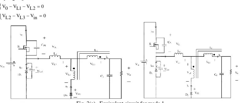
The ZCS-ZVS buck converter topology is shown in Fig.2. In this topology, inductors L1 and L2 are tightly coupled on the same ferrite core, and L1 is the main inductor. S1 and D1 are the main power switches, like a conventional buck converter.D2 is an additional diode. The theoretical current waveforms of L1, L2 , and L3 of the proposed converter at steady state are shown in Fig.3.When S1 is OFF, the converter comes into a free-wheeling stage. The branches of L2 and L3 will supply two flow channels for current freewheeling. Because L3 is very small, the current of L3 drops faster than that of L1 , and also reduces to zero before S1 turns ON. It provides the ZCS condition for S1 .
Due to snubber capacitor Cr1, S1 can turn OFF under a ZVS condition. Cp1 is the parasitic capacitance of the MOSFET S1.But here no extra auxiliary MOSFET switch is added, so the control method is as simple as that of a conventional buck converter. The theoretical waveforms of inductor currents and voltages are required to analyse the ZCS-ZVS buck converter in steady state. III.ANALYSES OF OPERATING PRINCIPLES
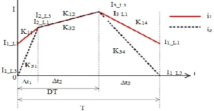
Based on the waveforms of the inductor currents.one switching cycle is divided into five intervals, as shown in Fig. 3,and the equivalent circuits for each interval are given in the section of corresponding modes of operation. Here Kij denotes theslopes of inductor current at a different mode, where i denotes the number of the inductor and j denotes the number of the different operating mode. The detailed theoretical analyses of each mode will be given as follows.
1)Mode 1[t0-t1]
Before t0 ,the converter works at a current free-wheeling stage, and both i3 and is1 are equal to zero. At t0, S1 is triggered to conduct. Due to L3, is1 will increase slowly, so S1 can turn ON under a ZCS condition. Then, i3 and i1 will increase, and i2 will go down. Since L3 is very small, the current-rising rate of L3 is larger than that of L1. At t1, i3 and i1 are equal, and i2 is zero. It means that D2 turns OFF automatically, and this mode ends. Based on KVL and KCL, we can get
0 in V 3 L V 2 L V 0 2 L V 1 L V 0 V 3 i 2 i 1 i (3)
Fig. 3(a). Equivalent circuit for mode 1 The voltage equations of inductors L1,L2 and L3 can be expressed as follows
dt 3 di 3 L 3 L V dt 1 di M dt 2 di 2 L 2 L V dt 2 di M dt 1 di 1 L 1 L V (4)
Where M is the mutual inductance and equal to
L
1L
2.
L1
L2 2M
L3 2 L 3 L 0 V 3 L M 2 L 2 L in V dt 1 di 11 K (5)
L1 L
2 2M
L3 3 L M 0 V 3 L M 1 L 1 L in V dt 2 di 21 K
L2 M
L3 2 L 0 V 3 L in V dt 3 di 31 K (7)
2) Mode 2 [t1-t2]
After t1, i3 and i1 are equal, and both increase linearly. In this mode, D2 is always OFF, and the branch of L2 does not work. At t2, S1 turns OFF, and this mode ends. It is similar to that of a conventional buck converter.
The slopes of i1, i2, and i3
Fig.3(b).Equivalent circuit for Mode2
0 22 K ; 3 L 1 L 0 V in V 32 K 12 K (8)
3) Mode 3[t2-t3]
At t2, S1 turns OFF, and then a resonance occurs between inductors (L1, L3), parasitic capacitor Cp1 , and snubber capacitors Cr1 . Cp1 is charged, and Cr1 is discharged at the same time. When the voltage across Cr1 reduces to zero, D1 will conduct. This interval is very short, so it is assumed that the current in L3 does not change in this mode. Because Cp1 is very small, it can be neglected. Thus, the transition time Tm1 can be obtained as follows.
Fig.3(d). Equivalent circuit forMode 4 Fig.3(c). Equivalent circuit for Mode 3
max
3
L
I
1
r
C
in
V
2
t
3
t
1
m
T
(9)where IL3 max,thevalue of i3 at t2 is positive and reaches a maximum in a switching cycle.
4) Mode 4 [t3-t4]
When D1 conducts, D2 will conduct simultaneously. The condition that D2 will conduct is shown in the following analyses. Firstly, it is assumed that D2 could not turn ON. The numbers of the turns of L1 and L2 are n1 and n2 , respectively, so
L
1
L
3
1
L
0
V
1
L
V
(10) Then3
L
1
L
1
L
0
V
1
n
2
n
1
L
V
1
n
2
n
2
L
V
L
1
L
3
M
0
V
3
L
1
L
1
L
0
V
1
L
2
L
(11)V0-VL1-VL2–VD=0 (12)
Substituting (10) and (11) into (12),we can obtain
3 1 3 0 2 D L L M L V V (13)
If D2 conducts VD2 must be less than zero.i.e.,the next inequality must be met L3<M (14) After t3, i3 will decrease much faster than i1 because L3 is comparatively small. As long as i3 reduces to zero,D1 will turn OFF, and the condition of ZCS for S1 is achieved. Then this mode naturally ends. After D2 conducts,VD2 is equal to zero.Based on KVL and KCL,we can get
0
V
V
0
V
V
V
i
i
i
3 L 2 L 3 L 1 L 0 3 2 1 (15)Substituting (4) into (15).the current slopes of the inductors are obtained as follows:
L1 L2 2M
L3 ) 2 L 3 L ( 0 V dt 1 di 14 K (16)
L
1
L
2
2
M
L
3
3
L
M
0
V
dt
2
di
24
k
(17)
L1 L2 2M
L3 ) M 2 L ( 0 V dt 3 di 34 K (18)
5) Mode 5 [t4-t5]
At t4,D1 turns OFF, thena small resonance between L3 and Cr1 occurs, in which i3 oscillates around zero and the amplitude is pretty small, so i3 issupposed to zero in this mode. Here, the currentjust flows through L1 and L2 , i.e., i1 is equal to i2. Therefore, the slopes of i1, i2, and i3 can be easily obtained as follows:
M
2
2
L
1
L
0
V
dt
1
di
15
K
(19)
M
2
L
L
V
dt
di
K
2 1
0 2
25
K35=0 (21)
III.DESIGNANDSIMULATIONS
A. Conventional Buck Converter The duty ratio is given by:
in out
V
V
D
(22)On substituting the values of input voltage and output voltage given in Table I in (22) we get D = 0.51. The value of capacitor and the inductor can be obtained from the relation below:
0
V
L
8
S
T
)
D
1
(
0
V
S
T
C
(23) ∆V0-Ripple voltage (0-10% of output voltage) and Ts=1\fs=2µs.Onsubstituting the values of Ts,V0,L and assuming ∆V0 = 0.141 and L from the Table I,the value of C is obtained as 100µF. R- Load resistance
C- Capacitance Ts-Switching Time period fs-Switching Frequency
L ΔI
L s
0 in
f
D
V
V
(24)
∆IL-Ripple current (0-30% of the load current). Similarly the value of inductor is obtained as 62.3µH.
The conventional buck converter is designed for a switching frequency of 50 kHz and a duty ratio of 0.51.The parameter values thus obtained are tabulated as shown below.
TABLE I
SIMULATION PARAMETERS OF CONVENTIONAL BUCK CONVERTER
Input Voltage 70V
Output Voltage 36V
Inductance 62.3µH
Capacitance 100µF
Resistive load 2.16Ω
Switching Frequency 50KHz
Fig. 4. Simulation of conventional buck converter
B. ZCS-ZVS Buck Converter with Coupled Inductor
To ensure that the ZCS-ZVS buck converter operates under the soft-switching condition,component parameters must be designed properly,especially the selections of the inductors(L1,L2 and L3).The current of L3 must be discontinuous to achieve soft-switching conditions.As the load increases,the duration that the current of L3 remains zero will reduce to zero,and then L3 will work at a continuous conduction mode(CCM) and discontinuous conduction mode(DCM) can be used to calculate the parameters of main circuits.It can be assumed that the buck converter would operate under BCM at a theoretic maximum load,which is more than the real maximum load.
Fig. 5. Theoretical waveforms of inductors currents at BCM.
TABLE II
RELATED TARGET SPECIFICATIONS OF THE ZCS-ZVSBUCK CONVERTER
Parameters Values
Vin 70 V
V0 36 V
Poutput_max 600 W
fSW 50 kHz
T 20µs
ILoad_Max_Real 16.7 A
ILoad_Max_Theoretic 18.4 A
I1_L1 14.72 A
I2_L1 17 A
I3_L1 22.08 A
I1_L3 0 A
I2_L3 17 A
The theoretical waveforms of inductor currents at BCM are shown in Fig. 5.In this design,the theoretic maximum load is set to be 1.1 times the real maximum load.In Fig. 5,it can be seen that mode 5 does not occur in BCM.Because the duration time of mode 3 is very short,it is not considered for calculating inductor parameters.One switching cycle can be divided into three intervals.Based on the slopes and variations of L1,L2,and L3,some equations can be obtained as in (25).
The Inductor currents of mode 1 and mode 3 are attained by the theoretical maximum load average current,and the ripple coefficient of the inductor current.T is the time of one switching period.Then ∆t1 ,∆t2,∆t3,L1,L2,and L3 can be solved
from (25),and the duty ratio D is equal to (∆t1+∆t2)/T.
3 L __ 3 I 3 L _ 1 I 3 t 34 K 1 L _ 3 I 1 L _ 1 I 3 t 14 K 1 L _ 2 I 1 L _ 3 I 2 t 12 K 3 L _ 1 I 3 L _ 2 I 1 t 31 K 1 L _ 1 I 1 L _ 2 I 1 t 11 K T 3 t 2 t 1 t (25)Fig. 6. Simulation of ZCS-ZVS buck converter
The related target specifications shown in Table II are substituted into (25),the solved results are presented in Table.III,where the basic equation in a buck converter as D = V0/Vin, is also meet in BCM.
TABLE III
SOLVED RESULTS OF INDUCTANCES AND DURATION TIMES
∆t1 0.623µs
∆t2 9.66µs
∆t3 9.71µs
L1 62.3µH
L2 1.49µH
L3 2.37µH
TABLE IV
SIMULATION PARAMETERS OF ZCS-ZVS BUCK CONVERTER
Sl. No. Components Ratings
1 DC Source 70 V
2 Output Voltage 36 V
2 Inductor L1 62.3 μH
3 Inductor L2 1.92μH
4 Inductor L3 1.4 μH
5 Snubber Capacitor Cr1 4700 pF
6 Output Capacitor C0 100 μF
7 Resistive Load R 2.16 Ω
The simulation parameters of ZCS-ZVS buck converter is shown in Table IV.
C. Simulation Results
The conventional buck converter and ZCS-ZVS buck converter was simulated using MATLAB/SIMULINK and the resulting waveforms are as shown below.
Fig. 7. Gate pulse, switch current and voltage waveform of conventional buck converter.
During the turn on process, after the gate trigger pulse is applied switch current increases and switch voltage decreases to zero which give rise to switching loss and during the turn off process switch current decreases to zero and switch voltage rises to a value equal to the input voltage which again give rise to switching losses which in turn reduces the efficiency of conventional buck converter. From the Fig. 7.it can be inferred that soft switching is not applicable here and the basic buck converter works under hard switching conditions. Switch suffers from high voltage and current stress under hard switching conditions.If a converter works under hard switching condition, switching losses increses at higher switching frequency and the total efficiencies will drop.
Here conduction losses will be high and efficiency will be poor at light loads. At higher switching frequency the switching losses will be high when compared to ZCS-ZVS buck converter.It can be inferred from the waveform that switching loss is more for a conventional buck converter which works under hard switching condition. Here soft switching technique cannot be adopted due to the absence of auxiliary circuits used to realize soft switching technique used in the ZCS-ZVS buck converter.
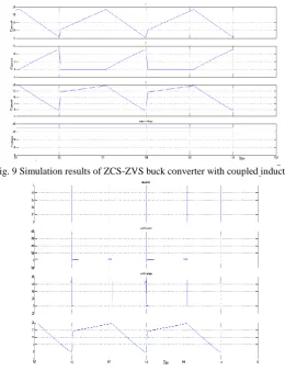
Fig. 9 Simulation results of ZCS-ZVS buck converter with coupled inductor.
Fig.10 Switching waveforms of Switch S1, and Current waveform of L3.
The simulation results of ZCS-ZVS buck converter with coupled inductor is shown in Fig. 9.The theoretical maximum load(18.4A)and the real maximum load(16.7A) along with the simulation waveforms of i1,i2,i3 are obtained from the parameters shown in Tables II and III.In Fig. 9,it can be seen that inductor L3 works under BCM and mode 5 does not occur for a theoretical maximum load. But for a real maximum load i3 remains zero in a short time and thereby ZCS turn on can be realized.
VI. CONCLUSION
The conventional buck converter and ZCS-ZVS buck converter were simulated using MATLAB/SIMULINK. The comparison between the both topologies was made. It was found that by making inductor L3 to work under DCM, ZCS turn on and ZVS turn off for S1 were achieved. Moreover no auxiliary MOSFET is added in this topology, so the control method is as simple as that of conventional buck converter. The low efficiency problem at light loads can be solved easily using the ZCS-ZVS buck converter with coupled inductor topology than the conventional buck converter.
REFERENCES
[1] Lei Jiang, Chunting Chris Mi,Siqi,Li,Chengliang Yin, and jinchuan Li, “An improved soft switching buck converter with coupled inductor,”
[2] M.R.Mohammadi and H. Farzanehfard, “New family of zero- voltage transition PWM bidirectional converters with coupled inductors,” IEEE Trans. Ind. Electron., vol. 59,no. 2,,pp. 912–919, Feb. 2012.
[3]M. Jabbari and H. Farzenehfard,“New resonant step-down/up converters,” IEEE Trans. Power. Electron., vol.25, no. 1, pp. 249–256,Jan. 2010.
[4]S.Urgan,T. Erfidan, H. Bodur, and B. Cakir, “A new ZVT-ZCT quasi-resonant DC link for soft switching inverters,” Int.J.Electron., vol. 97, no. 11, pp. 83–97, 2010.
[5]J. Zhang,J.-S. Lai,R.-Y. Kim and W.Yu, “High power density design of a soft-switching high power bidirectional dc-dc converter,” IEEE Trans.
Power Electron., vol. 22, no. 4, pp. 1145–1153, Jul. 2007.
[6]H. Bodur and A.F. Bakan,“An improved ZCT-PWM DC-DC converter for high-power and frequency applications,” IEEE Trans. Ind. Electron., Vol. 51,no. 1,pp.89–95, Feb. 2004.