University of Windsor University of Windsor
Scholarship at UWindsor
Scholarship at UWindsor
Electronic Theses and Dissertations Theses, Dissertations, and Major Papers
Fall 2017
Phase Locking Authentication for Scan Architecture
Phase Locking Authentication for Scan Architecture
Donatus Silva Richard University of Windsor
Follow this and additional works at: https://scholar.uwindsor.ca/etd Part of the Engineering Commons
Recommended Citation Recommended Citation
Richard, Donatus Silva, "Phase Locking Authentication for Scan Architecture" (2017). Electronic Theses and Dissertations. 7338.
https://scholar.uwindsor.ca/etd/7338
This online database contains the full-text of PhD dissertations and Masters’ theses of University of Windsor students from 1954 forward. These documents are made available for personal study and research purposes only, in accordance with the Canadian Copyright Act and the Creative Commons license—CC BY-NC-ND (Attribution, Non-Commercial, No Derivative Works). Under this license, works must always be attributed to the copyright holder (original author), cannot be used for any commercial purposes, and may not be altered. Any other use would require the permission of the copyright holder. Students may inquire about withdrawing their dissertation and/or thesis from this database. For additional inquiries, please contact the repository administrator via email
Phase Locking Authentication for Scan Architecture
By
Donatus Silva Richard
A Thesis
Submitted to the Faculty of Graduate Studies
through the Department of Electrical and Computer Engineering
in Partial Fulfillment of the Requirements for
the Degree of Master of Applied Science
at the University of Windsor
Windsor, Ontario, Canada
2017
Phase Locking Authentication for Scan Architecture
by
Donatus Silva Richard
APPROVED BY:
______________________________________________
R. Riahi
Mechanical, Automotive & Materials Engineering
______________________________________________
R. Muscedere
Department of Electrical and Computer Engineering
______________________________________________
M. Ahmadi, Co-Advisor
Department of Electrical and Computer Engineering
______________________________________________
R. Rashidzadeh, Co-Advisor
Department ofElectrical and Computer Engineering
iii
DECLARATION OF ORIGINALITY
I. Co-Authorship
I hereby declare that this thesis incorporates material that is result of research conducted under the supervision of Dr. Rashid Rashidzadeh and Dr. Majid Ahmadi. Chapter 3 of the thesis was co-authored with Mr. Yahia Ouahab under the supervision of Dr. Rashid Rashidzadeh. In all cases the key ideas, experimental designs, data analysis, interpretation and writing were performed by both the author and co-author. I am aware of the University of Windsor Senate Policy on Authorship and I certify that I have properly acknowledged the contribution of other researchers to my thesis, and have obtained written permission from each of the co-authors to include the materials in my thesis.I certify that, with the above qualification, this thesis, and the research to which it refers, is the product of my own work.
II. Previous Publication
This thesis includes three original papers that have been previously published/submitted for publication in peer reviewed journals, as follows:
Chapter Publication Title Publication Status
Chapter -3 Y. Ouahab, D. S. Richard, and R. Rashidzadeh, “Secure scan chain using test port for tester authentication,” in 2016 IEEE International Conference on Electronics, Circuits and Systems, ICECS 2016, 2017.
Published
Chapter -4 D. S. Richard, R. Rashidzadeh, M. Ahmadi, “Secure Scan Chain using a Phase Locking
Authentication Technique” IEEE International Symposium on Signals, Circuits and Systems (ISSCS) Romania, 2017.
iv
Chapter -5 D. S. Richard, R. Rashidzadeh, M. Ahmadi, “Secure Scan Architecture Using Clock and Data Recovery Technique,”
Prepared, to be submitted to ISCAS 2018
I certify that I have obtained a written permission from the copyright owner(s) to
include the above published material(s) in my thesis. I certify that the above material
describes work completed during my registration as a graduate student at the
University of Windsor.
III. General
I declare that, to the best of my knowledge, my thesis does not infringe upon
anyone’s copyright nor violate any proprietary rights and that any ideas, techniques,
quotations, or any other material from the work of other people included in my
thesis, published or otherwise, are fully acknowledged in accordance with the
standard referencing practices. Furthermore, to the extent that I have included
copyrighted material that surpasses the bounds of fair dealing within the meaning of
the Canada Copyright Act, I certify that I have obtained a written permission from
the copyright owners to include such materials in my thesis.
I declare that this is a true copy of my thesis, including any final revisions, as
approved by my thesis committee and the Graduate Studies office, and that this
thesis has not been submitted for a higher degree to any other University or
v
ABSTRACT
Scan design is a widely used Design for Testability (DfT) approach for digital
circuits. It provides a high level of controllability and observability resulting in a
high fault coverage. To achieve a high level of testability, scan architecture must
provide access to the internal nodes of the circuit-under-test (CUT). This access
however leads to vulnerability in the security of the CUT. If an unrestricted access
is provided through a scan architecture, unlimited test vectors can be applied to the
CUT and its responses can be captured. Such an unrestricted access to the CUT can
potentially undermine the security of the critical information stored in the CUT.
There is a need to secure scan architecture to prevent hardware attacks however a
secure solution may limit the CUT testability. There is a trade-off between security
and testability, therefore, a secure scan architecture without hindering its
controllability and observability is required. Three solutions to secure scan
architecture have been proposed in this thesis.
In the first method, the tester is authenticated and the number of authentication
attempts has been limited. In the second method, a Phase Locked Loop (PLL) is
utilized to secure scan architecture. In the third method, the scan architecture is
secured through a clock and data recovery (CDR) technique. This is a manuscript
based thesis and the results of this study have been published in two conference
proceedings. The latest results have also been prepared as an article for submission
vi
DEDICATION
Learning is excellence of wealth that none destroy;
To man nought else affords reality of joy. -Thiruvalluvar
Education is the true imperishable riches; all other things are not riches.
I dedicate my work to my parents, Mr. Richard Silvester and Mrs. Alex Majella
Richard and my grandparents. Thank you for always being there. Thank you for
the indestructible wealth of all time. I would also like to thank my family for their
vii
ACKNOWLEDGEMENTS
I would like to sincerely thank my supervisor, Dr. Rashid Rashidzadeh, for his
guidance and support in successfully completing my thesis. I am deeply grateful for
his involvement in all my work, guiding me, mentoring me and providing me with
any help that I needed to complete my degree. It is an honor to have worked under
his supervision.
I am grateful to my co-supervisor Dr. Majid Ahmadi for his support and valuable
comments which helped in completing this thesis.
I would also like to thank my committee members Dr. Roberto Muscedere and Dr.
Reza Riahi for their, encouragement, constructive comments and positive criticism
which in fact improved my ideas and solutions.
I would like to extend my gratitude to my colleagues at the Research Centre for
Integrated Microsystems (RCIM). I appreciate their friendship, support,
encouragement, their constant involvement and valuable feedback.
Finally, I would like to thank the research and financial support received from
Natural Sciences and Engineering Research Council (NSERC) of Canada and CMC
viii
TABLE OF CONTENTS
DECLARATION OF ORIGINALITY ... iii
DEDICATION ... vi
ACKNOWLEDGEMENTS ... vii
LIST OF TABLES ... xi
LIST OF FIGURES ... xii
LIST OF ABBREVIATIONS/SYMBOLS ... xiv
Chapter -1 ... 1
Introduction ... 1
1.1 Testing a Device ... 3
1.2 Test During VLSI Manufacturing Process ... 5
1.3 Problem Statement: Need for Hardware Security ... 7
1.4 Research Objectives ... 7
1.5 Thesis Overview ... 8
1.6 References ... 9
Chapter -2 ... 11
Design for Testability ... 11
2.1 Ad Hoc ... 12
2.2 Built-In-Self-Test ... 13
2.3 Scan Architecture ... 14
2.3.1 Scan Cells or Scan Flip-Flops. ... 15
2.3.2 Scan Chain ... 15
2.3.3 Joint Test Access Group (JTAG) Port ... 16
2.3.4 Scan based Testing ... 17
2.3.5 Boundary Scan Testing ... 18
2.4 References ... 19
Chapter -3 ... 21
ix
3.1 Introduction ... 21
3.2 Proposed Solution ... 24
3.2.1 Tester Authentication Block ... 25
3.2.2 Scan based attacks ... 26
3.2.3 Secure scan chain ... 27
3.3 Implementation ... 29
3.4 Comparative analysis ... 31
3.5 Conclusion ... 32
3.6 References ... 33
Chapter-4 ... 36
Secure Scan Chain using a Phase Locking Authentication Technique ... 36
4.1 Introduction ... 36
4.2 Scan Based Attack: ... 39
4.3 Proposed Solution For Secure Scan Architecture In 3D-IC... 40
4.3.1 Phase Locked Loop (PLL) ... 41
4.3.2 Secure scan chain ... 42
4.4 Implementation And Simulation Results ... 43
4.5 Comparative Analysis ... 46
4.6 Conclusion ... 47
4.7 References ... 48
Chapter-5 ... 51
Secure Scan Architecture Using Clock and Data Recovery Technique ... 51
5.1 Introduction ... 51
5.2 Scan Based Attack ... 53
5.3 Proposed Solution for Scan Architecture ... 54
5.3.1 Clock and Data Recovery(CDR) ... 56
5.3.2 Delay Locked Loop ... 57
5.3.3 Authentication Block ... 58
5.4 Implementation ... 59
5.5 Security Analysis ... 62
5.6 Conclusion ... 64
x
Chapter -6 ... 67
Conclusions and future work ... 67
6.1 Conclusions ... 67
6.2 Future Works ... 68
APPENDIX :COPY RIGHT PERMISSION... 69
xi
LIST OF TABLES
Table 1: JTAG Boundary Scan Interface Based on IEEE Standard
1149.1………..16
Table 2: Area overhead measurements………...…….29
xii
LIST OF FIGURES
Figure- 1 Testing at various levels of Manufacturing………..………...2
Figure- 2 Overview of Testing……….………..5
Figure- 3 Testing during VLSI Development Process……….…….…………..5
Figure- 4 Ad Hoc with MUX as insertion point at (a) input of internal node and (b) output of internal node……….……….…...12
Figure- 5 A Basic BIST Structure……….………...13
Figure- 6 Scan cell or a Scan Flip-Flop……….………...15
Figure- 7 Structure of a Scan chain……….……….15
Figure- 8 Testing using Scan Architecture……….………..17
Figure- 9 Boundary Scan Architecture [7]……….………..18
Figure- 10 Tester Authentication block diagram………..……....23
Figure- 11 Two phases of test port for authentication………....……...24
Figure- 12 Tester Authentication Block constitution……….……..25
Figure- 13 Hardwired flip-flops with BIST to store encryption key………..……...28
Figure- 14 Area overhead of the authentication block………..………29
xiii
Figure- 16 Components of DUT……….………….39
Figure- 17 PLL Block Diagram……….…………..42
Figure- 18 Hardwired flip-flops with BIST to store encryption key [13]..………...43
Figure- 19 PLL Frequency synthesis with divide by 2 frequency divider...………..44
Figure- 20 Output response when the tester and the DUT are in a locked state…….45
Figure- 21 A sample of the output response when the tester and the DUT are not in a locked state Scenario 2……….………..…...45
Figure-22 Scan architecture………...53
Figure- 23 The frequency matching process involving PLL……….…...55
Figure- 24 Components of DUT……….……….55
Figure- 25 CDR Block Diagram……….……….…56
Figure- 26 DLL Block Diagram………..……….…57
Figure- 27 Authentication Block Diagram………...58
Figure- 28 DLL clock recovery with Charge pump in locked state………..59
Figure- 29 Manchester encoding of 8-bit data………..60
Figure- 30 Decoded data using 40MHz clock………..60
xiv
LIST OF ABBREVIATIONS/SYMBOLS
Abbreviations/Symbols Description IC VLSI SOC ATPG RNG CUT DUT DfT ATE BIST ORA PCB SFF SC PLL DLL CDR PFD VCO Integrated Circuit
Very Large-Scale Integration
System on Chip
Automatic Test Pattern Generator
Random Number Generator
Circuit Under Test
Device Under Test
Design for testability
Automatic Test Equipment
Built-In-Self-Test
Output Response Analyzers
Printed Circuit Board
Scan Flip-Flops
Scan Cell
Phase Locked Loop
Delay Locked Loop
Clock and Data Recovery
Phase Frequency Detector
xv VCDL CP LPF TAP JTAG MUX SDI SDO TDI TDO TMS TCK MKR 3D-IC TSV
Voltage Controlled Delay Line
Charge Pump
Low Pass Filter.
Test Access Port
Joint Test Action Group
Multiplexer
Scan Data In
Scan Data Out
Test Data In
Test Data Out
Test Mode Select
Test Clock
Mirror Key Register
3-Dimensional Integrated Circuit
1
Chapter -1
Introduction
Integrated Circuits (ICs) have advanced steadily from Small Scale Integration (SSI)
devices to Very Large-Scale Integration (VLSI) devices. This progression in the reduction
of the size of ICs has followed the Moore’s law. Moore’s law states that the number of
transistors in an IC doubles every 18 months. VLSI devices nowadays have hundreds of
millions of transistors on them. Most chips that are used in computers and electronics
devices contain millions of transistors. This is due to the reduction in feature size of
transistors. Interconnecting wires used in these devices have also seen a significant
reduction in thickness. The current wires are in the scale of nanometers. These reductions
in dimensions allow transistors to be compacted in a small area leading to smaller chips.
Smaller chips are faster and have lower power consumption. Current ICs have operating
frequencies in the range of several gigahertz.
The size of IC plays a major factor in defects that may occur during their manufacturing
processes. The probability of defect occurring in an IC increases with its size reduction.
Transistors in an IC can become faulty even if there is a minute defect. It takes a single
defective transistor to make the entire IC faulty. Manufacturing defects are inevitable,
therefore some of the manufactured ICs will be flawed. Testing is required to weed out the
faulty ICs from the fault free [1].
The cost of developing integrated circuits is high. There is a rule of ten which states that
the cost of detecting faults in an IC increases by magnitude as we move through the various
2
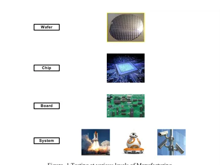
Figure 1. The cost of testing will increase as we move up from ICs to Printed Circuit Boards
(PCBs) and PCBs to system level. The system level may contain many PCBs, which will
further increase the cost of testing. Aside from manufacturing phase, integrated circuits
need to be tested prior to releasing them to the market. These requirements prompted the
development of testing techniques that allows ICs to be tested at various manufacturing
stages and during system operation. These techniques are called Design for Testability
(DfT).
Figure -1 Testing at various levels of Manufacturing Wafer
Chip
Board
3
1.1Testing a Device
Testing a circuit requires external stimuli to be applied to the circuit. These stimuli are in
the form of binary inputs called test vectors or test patterns. For a circuit with inputs,
n-bit test vectors must be applied to obtain responses. There are many testing techniques
available which can be categorized into two types: functional and structural testing. In
functional testing, as the name suggests the function of the Circuit Under Test (CUT) is
tested. If the CUT performs its function properly then the CUT is said to be fault free. For
a CUT with n-bit input, all possible 2n test vectors can be applied. If the correct responses
are produced for the applied test vectors then the CUT is fault free. This method covers
most of the fault models and faulty circuits can detected. However, when functional testing
is performed, the type of fault that is in the CUT cannot be determined. The time taken to
test are usually high for those CUTs with a high number of inputs.
Structural testing on the other hand employs specific test vector for a set of fault models
based on the structural information of the CUT. Only these test vectors are applied to the
CUT to obtain the responses. Structural testing is less time consuming compared to the
functional testing. However, a structural test can only cover the defects that are modeled
since the test vectors are generated using the fault models. It cannot detect any other faults
in the CUT [3].
Various faults that occur during the manufacturing process of the CUT are modeled by
different fault models. Test vector generated based on these models stimulate the CUT to
detect the defects in the CUT. There are two criteria under which a fault model should be
4
1) The behavior of the defect must be accurately reproduced by the fault model
2) It should efficiently simulate the fault and produce test vectors based on the fault.
The area of the circuit where faults occur are called fault sites. At each potential fault site,
different faults can occur which can be bunched together into one single fault model.
Assuming that there are n possible fault sites in a CUT and k different types of faults, there
are two types of fault models: single fault model and multiple fault model. In the single
fault model, there is only one type of fault that occurs in the CUT. The total number of
possible faults is:
Number of single faults = k × n (1)
Multiple fault models consist of different types of faults but each model can contain at most
2 types of fault in them (k=2). The total number of possible faults in this case is:
Number of multiple faults = (k+1)n -1 (2)
Equation (2) shows the realistic approach to calculating the number of possible faults in a
circuit since any number of faults may occur during the manufacturing process. While
generating test vectors to test a circuit multiple fault models can be taken into account [4,8].
Test vectors can be generated using Automatic Test Pattern Generators (ATPG) [5]. These
ATPGs utilize algorithms that produce test vectors with a high fault coverage. They can be
configured to produce specific test vectors for fault models or the entire truth table of the
n-bit input for a more exhaustive testing. The simplest way to generate a test vector is a
Random Number Generator (RNG). However, it does not generate test vectors based on
5
Most devices are tested by Automatic Test Equipment (ATE) [6]. These ATEs have
advanced processing units, pin electronics and fixtures to apply stimuli to the CUT. They
also have ATPGs to generate the test vectors based on the type of testing that needs to be
performed and Output Response Analyzers (ORA) to verify the responses. The devices
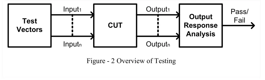
that produce correct responses are fault-free [7]. An overview of testing has been illustrated
in Figure 2.
1.2Test During VLSI Manufacturing Process
VLSI devices are tested at various stages of their manufacturing process. They are tested
during development process, electronic system manufacturing process and system level Figure - 2 Overview of Testing
Test Vectors CUT Output Response Analysis Input1 Inputn Output1 Outputn Pass/ Fail
6
operation. During development process, the function of the VLSI device based on the
customer requirement is formulated and a circuit is synthesized based on the design
specifications. Then design verification takes place, where the circuit design is analyzed to
predict its function before the fabrication process. The fabricated ICs are then tested for
faults that may have occurred during fabrication processes at wafer level. Fault free ICs are
the packaged and tested once again for any defect caused by packaging process or by a
defective package. Before shipping, final test is conducted to assure the IC quality. This
process is shown in Figure 3. Since faulty ICs are unavoidable during the manufacturing
process, yield and reject rates are necessary to minimize the loss. Yield is defined as the
percentage of acceptable parts among all parts that are fabricated. In some cases, a faulty
IC may appear functional and pass the final test. Reject rate is the number of faulty parts
passing the final test among the total number of parts passing final test. An acceptable
reject rate is 500 parts per million (PPM). Reject rate of 100PPM or below is a high quality
manufacturing process. DfT techniques are commonly utilized to reduce the reject rate [8].
Electronic systems are made up of one or more Printed Circuit Boards (PCBs) which hosts
VLSI devices. These PCBs need to be tested after fabrication for any defects before
mounting any VLSI devices on them. Once the PCB is assembled, further tests are
performed to check for any faults. The tested PCBs are then assembled into units and
systems that are tested prior to shipping [8].
Electronic systems are often tested on field from time to time to ensure that the systems
are in working condition. DfT techniques provide a way to test the devices at various
staged of the manufacturing process. DfT techniques have been explained in detail in
7
1.3 Problem Statement: Need for Hardware Security
Testing techniques play a vital role in detecting faults and producing fault free circuits.
Testing techniques like DfT provide a high level of access to the circuits to conduct
extensive and efficient testing. DfT techniques offer controllability and observability over
Device Under Test (DUTs). However, this level of access leaves the circuit vulnerable to
an attack. DfT techniques can be used as a pathway to gaining sensitive information that
are stored in the circuit. For example, consider a device consisting of a crypto-core with a
DfT architecture embedded in it during the development process. Attackers can access the
crypto-core through the DfT architectures and obtain the secret key in the crypto-core.
Hence it is necessary to prevent such attacks from happening. To do so, secure DfT
technique should be designed. There is a trade-off between testing and security. To test a
device completely for any kind of faults, complete and unrestricted access is required.
However, securing a DfT technique may restrict the tester from having complete access to
the DUT which is needed to perform the necessary tests. The focus of this thesis is on scan
architecture, one of the widely used DfT techniques. Three different solutions have been
proposed to protect hardware devices against scan-based attacks without limiting
controllability and observability.
1.4 Research Objectives
The objective of this research is to design a secure scan architecture against scan-based
attacks without compromising the controllability and observability.
8
1. In the first solution, a secure scan chain using test port for tester
authentication has been proposed. The CUT requires an authentication code to grant
access to the scan architecture and limits the number of trials to enter the
authentication code.
2. In the second solution, a secure scan architecture using Phase Locking
Authentication has been proposed. User authentication is achieved using a Phase
Locked Loop. To access the scan chain the user must synchronize with the CUT.
This solution has been implemented and simulation results are presented. Phase
locking authentication also serves as a viable solution for 3D ICs.
3. The third solution involves the Clock and Data Recovery technique used to
authenticate the user. The CUT requires the user to know its operating frequency,
authentication key and the line coding used to merge the data and the clock.
1.5 Thesis Overview
This thesis is organized as follows:
Chapter-1 gives a brief overview of why testing is important, how to test a device and the
testing involved during a VLSI development process. It also presents the problem statement
and the solutions proposed to address the problem statement.
Chapter -2 provides insight on Design for Testability (DfT) techniques that are available
with a focus on scan architectures. It also describes scan based attacks and a brief overview
of existing security measures has.
Chapter-3 presents the first solution proposed for a secure scan architecture. Secure scan
9
been published as a paper in IEE International conference on Electronics Circuits and
Systems (ICECS) 2016, ISBN-978-1-5090-6113-6.
Chapter-4 explains the second solution proposed for a secure scan architecture. Secure scan
chain usinga Phase Locking Authentication Technique has been published as a paper in
IEEE International Symposium on Signals, Circuits and Systems (ISSCS) 2017.
In chapter-5 a solution to authenticate users based on lock and key method, clock
synchronization and line coding technique has been proposed. The proposed work has been
prepared to be submitted to ISCAS 2018.
Chapter-6 covers conclusion and future works.
1.6 References
[1] G. Moore, “Cramming more components onto integrated circuits”, Electronics, vol 38,
no (8), pp 114–117, 1965.
[2] Davis B, “The Economics of Automatic Testing”, McGraw-Hill, London, United
Kingdom, 1982.
[3] M. Tehranipoor, C. Wang, " Background on VLSI Testing," Introduction to Hardware
Security and trust., pp. 1-26, 2006.
[4] C. Stroud, J. Emmert, and J. Bailey, A new bridging fault model for more accurate fault
behavior, in Pro. Automat. Test Conf. (AUTOTESTCON), September 2000, pp. 481–485.
[5] J. Roth, Diagnosis of automata failures: A calculus and a method, IBM J. Res. Develop.,
10
[6] A.C. Strover, ATE: Automatic Test Equipment, New York, McGraw Hill, 1984.
[7] M. Abramovici, M. A. Breuer, and A. D. Friedman, Digital Systems Testing and
Testable Design, IEEE Press, Piscataway, NJ, 1994 (revised printing).
[8] L. T. Wang, C. W. Wu and X. Wen, " Introduction," VLSI Test Principles and
Architectures., pp. 1-36, 2006.
[9] P. Goel, “An implicit enumeration algorithm to generate tests for combinational
11
Chapter -2
Design for Testability
Design for Testability (DfT) can be defined as the integration of testing capabilities into
the design of a circuit. DfT solutions are included in the design of a circuit during the
development process. DfT techniques are developed to test the circuit at a given stage of
the manufacturing process. They provide access to the internal nodes of the circuit. Without
DfT techniques test solutions with a high fault coverage become a major challenge. DfT
techniques provide support for structural testing. They increase the circuit controllability
and observability considerably. To test a circuit, the tester has to able to control the internal
nodes of CUT to apply test vectors and observe its responses. There are various DfT
techniques but they can be categorized into three main types: (1) Ad Hoc, (2)
Built-in-Self-Test (BIST) and (3) Scan architecture [1]. This chapter will briefly discuss Ad Hoc and
BIST. Scan architecture will be discussed in detail as the focus of this thesis is on a secure
12
2.1 Ad Hoc
Ad hoc techniques are implemented by adding extra circuitry to test parts of the circuit that
are difficult to access. This extra circuitry allows the tester to control and observe the
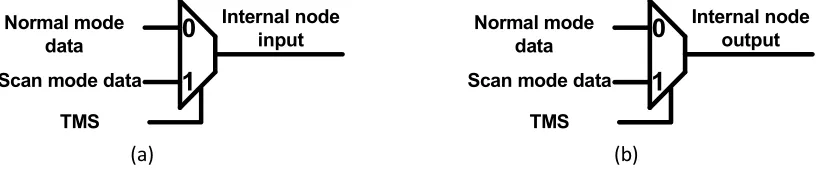
internal nodes in the target area. Test point insertion is a typical example of Ad hoc. It is
used to improve the controllability and observability of the circuit. Test point insertion can
be metalized by adding a multiplexer at an input or an output node. The multiplexers
(MUX) can be used to apply test data and capture the responses of desired nodes. Figure
4(a) and 4(b) shows a MUX used at the input and the output nodes of a circuit-under-test
[2]. Adding extra circuitry to the CUT increases the overhead area. Moreover, to access the
test insertion points probes are used.
(a) (b)
Figure -4 Ad Hoc with MUX as insertion point at (a) input of internal node and (b) output of internal node.
0
1
TMSNormal mode data Scan mode data
Internal node input
0
1
TMS Normal mode data Scan mode data13
2.2 Built-In-Self-Test
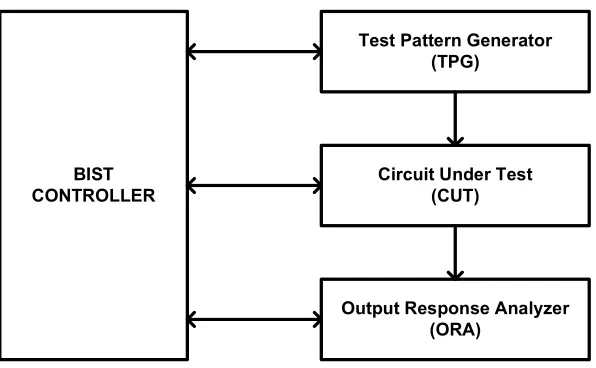
Built-In-Self-Test (BIST) technique enables a circuit to test itself and produce a pass/fail
output without any stimuli from an outside source. BIST consists of a BIST controller, Test
Pattern Generator (TPG) and an Output Response Analyzer (ORA). The TPG generates
test vectors to be applied to the CUT. The ORA commonly compacts the output responses
of the CUT into a signature. The BIST controller coordinates the TPG, CUT and ORA by
synchronizing them. It also provides a golden signature that is the correct output response
for the test vector applied. The signature provided by the ORA is compared with the golden
signature. Once the comparison is done, the BIST controller provides a pass/fail result.
Since the output is only a pass/fail indication, it is not possible to determine the type of
fault that is present in the circuit or where the fault has occurred. The area overhead of the
circuit increases with the addition of BIST to the circuit. The BIST can be present near the
target circuit or away from it on the board in which the circuit is embedded. Figure 5 shows
a typical BIST.
Figure -5 A Basic BIST Structure
Test Pattern Generator (TPG)
Circuit Under Test (CUT)
Output Response Analyzer (ORA)
14
2.3 Scan Architecture
Scan Design is a widely used DfT techniques. Scan architecture utilizes flip-flops that are
present in the circuit. By adding extra logic to the flip-flops, they are converted to a
scannable flip-flops. These modified flip-flops are called Scan Cells (SCs) or scan flip-flop
(SFFs). A number of scan flip-flops are connected properly together to form a shift register.
The shift registers are called scan chain. This DfT technique allows the tester to switch
between operation mode and test mode. Scan architecture provides a high controllability
and observability since SFFs provide access to the internal nodes of the circuit-under-test.
The SFFs can be inserted at any internal node of the circuit during the design phase. If
SFFs are inserted into part of the circuit that are difficult to test during the design phase,
the observability and the controllability of the CUT increases leading to a high fault
coverage. There are two modes of operations for scan architecture: 1) Normal mode of
operation where the input of the circuit can be any logic data depending on the function of
the circuit and 2) Test mode where test vectors are applied through scan chain to the CUT
and its responses are observed. On board level and system level, accessing scan chains
become difficult due to the pin configurations on each circuit. To overcome this limitation,
boundary scan technique was introduced by Joint Test Action Group (JTAG) which utilizes
15
2.3.1 Scan Cells or Scan Flip-Flops.
Scan Flip-Flops are typically made up of Multiplexers and D flip-flops as illustrated in
Figure 6. The multiplexers in SFF allow the tester to choose between test input and data
input. SFFs can be switched between the normal mode and the test mode [6].
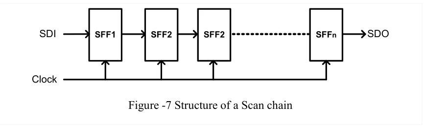
2.3.2 Scan Chain
A scan chain is a shift register made of Scan Flip-Flops as shown in Figure 7. Test vectors
are applied to the scan chain through Scan Data In (SDI) to test the circuit and the responses
are obtained from Scan Data Out (SDO) [7]. These pins are accessed through JTAG port,
which also controls the transition between the normal mode and the test mode. Figure -6 Scan cell or a Scan Flip-Flop
Figure -7 Structure of a Scan chain
SFF1 SFF2 SFF2 SFFn SDO
SDI
16
2.3.3 Joint Test Access Group (JTAG) Port
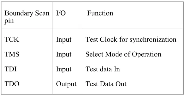
JTAG introduced Test Access Port (TAP) as IEEE standard 1149.1, which is used at the
board level and the system level to access scan chains [8]. TAP consists of a four-wire
serial bus interface through which the mode of operation for the boundary scan is
controlled. TAP provides access to the scan chain through four pins shown in table I. The
TCK pin provides the test clock to synchronize the tester and the scan chain. TMS selects
the mode of operation. It controls the MUX in SFFs. Test vectors can be applied through
TDI pin and their responses are obtained through TDO. TAP is also popularly known as
JTAG port which serves as interface to access and test various system level devices [9]. Table I: JTAG Boundary Scan Interface Based on IEEE Standard 1149.1
Boundary Scan
pin I/O Function
TCK
TMS
TDI
TDO
Input
Input
Input
Output
Test Clock for synchronization
Select Mode of Operation
Test data In
17
2.3.4 Scan based Testing
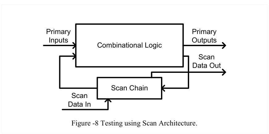
Figure 8 shows a combinational circuit with the scan architecture embedded in it. In the
normal operation mode, the CUT performs its function on the supplied input without any
intervention from outside source and the response is obtained. In the test mode, the test
vectors can be applied to any internal node of the circuit with the help of scan architecture
[10]. The process involved in scan based testing is summarized below:
Scan in: The CUT is switched to test mode and the test vectors are shifted or scanned into
the scan chain to be applied to the circuit-under-test.
Capture mode: The test vectors are applied to the CUT and the CUT is switched back to
the normal mode to perform its operations. Once the CUT completes its function, it is then
switched to test mode and the output responses are recorded in the scan chain:
Scan out: The output responses are then scanned out to be analyzed to check if any part of
the CUT is faulty. A pass/fail result can be inferred from the analysis. Figure -8 Testing using Scan Architecture.
Combinational Logic
Scan Chain Primary
Inputs
Primary Outputs
Scan Data In
18
2.3.5 Boundary Scan Testing
PCBs have many VLSI circuits mounted on them and systems have many PCBs assembled
in them. If all ICs in the PCBs and system have scan architecture built in them, they are
difficult to test due to limited access at the board level. This is because there are no
configurations on the PCBs to access the scan chain in each individual ICs. To overcome
this difficulty boundary scan was introduced. Boundary scan provides access to the input
and the output pins of all ICs on a PCB by connecting SFFs to them and forming a scan
19
scanned in through the scan chain and applied to the target IC’s input pins and the responses
are obtained for fault analysis. Boundary scan uses JTAG port as an interface to perform
tests. Boundary scan also provides access to DfT techniques embedded in individual ICs
in PCBs [11].
2.4 References
[1] L. T. Wang, C. W. Wu and X. Wen, "Design for Testability," VLSI Test Principles and
Architectures., pp. 37-104, 2006.
[2] M. Abramovici, M. A. Breuer, and A. D. Friedman, Digital Systems Testing and
Testable Design, IEEE Press, Piscataway, NJ, 1994.
[3] C. E. Stroud, A Designer’s Guide to Built-In Self-Test, Springer Science, Boston,MA,
2002.
[4] L. T. Wang, C. W. Wu and X. Wen, "Logic Built-In Self-Test," VLSI Test Principles
and Architectures., pp. 263-340, 2006.
[5] T. W. Williams and K. P. Parker, Design for testability: A survey, Proc. IEEE, 71(1),
98–112, 1983.
[6] E. B. Eichelberger and T. W. Williams, A logic design structure for LSI testability, in
Proc. Des. Automat. Conf., June 1977, pp. 462–468.
[7] M. Tehranipoor, C. Wang, " Background on VLSI Testing," Introduction to Hardware
20
[8] IEEE Standard 1149.1–2001 (2001) Standard test access port and boundary-scan
architecture. IEEE Standards Board.
[9] Oshana R (2002) Introduction to JTAG. In: EE Times Design, 29 October 2002
[10] Bushnell ML, Agrawal VD (2000) Essentials of Electronic Testing for Digital,
Memory, and Mixed-signal VLSI Circuits. Kluwer Academic Publishers, Dordrecht
(Hingham, MA)
[11] L. T. Wang, C. W. Wu and X. Wen, " Introduction," VLSI Test Principles and
21
Chapter -3
Secure Scan Chain using Test Port for Tester Authentication
3.1Introduction
Test engineers seek for greater controllability and observability in order to manage test
stimuli and observe the responses. Scan architecture is known as an effective DfT measure
for digital circuits. Scan chains are used to increase the testability of circuits to apply test
vectors and observe their responses. However, scan architecture can also be used as a back
door for hackers to break down a chip security [2]. Scan architecture has been used to hack
various crypto hardware implementations such us AES, RSA etc. A secure scan
architecture to protect CUT against scan-based attacks while maintaining a high
controllability and observability has become a design requirement. There are two
commonly used methods to provide security for scan architecture against potential attacks.
First, the access to the scan chain is restricted using a private controller. Second, the access
to the scan chain is open; however, the data are encrypted [3]. Many solutions to protect
crypto cores against the scan chain attacks have been reported in the literature. In [4] access
to the scan chain is granted only if a predetermined key is entered. Test patterns are used
as the authentication keys to allow access to the scan chain [5]. A function/test mode
control method has been proposed in [6]. It limits the transitions between normal function
mode and the test mode for crypto cores. However, this method is not suitable for at-speed
online testing.
The second secure scan architecture method allows access to the scan chain but during the
22
different methods such as adding gates like invertor, XORs, XNORs or scrambling the scan
chain. Various encryption methods are used to encrypt the actual scanned output and make
the output data as random as possible so that the attacker is unable to deduce the secret
keys of the crypto cores. A secure scan architecture using the second method is the flipped
scan technique [7]. In this technique, inverters are randomly placed in the scan chain to
confuse the attacker, as the locations of the invertors in the scan chain are not known to the
attacker. Although, it is difficult to guess the location of the invertors but a “reset” attack
on the system can reveal the location of the invertors. When the flip flops are reset, the
scan out become a stream of zeroes with ones indicating the locations of invertors.
Another secure scan architecture is the random placement of XORs between scan cells [8].
This serves to confuse attacker as the nature of the gates inserted would be unclear and the
attacker might not consider the possibility. This method offers better security than the
above technique since this method passes the “reset” attack. Most of the available solution
for a secure scan architecture allow the testers to access the scan chain, apply test vectors
and observe the output responses. Moreover, the access to the scan chain is not limited and
tests can be performed any number of times. Therefore, there is a possibility of access to
critical information through analysis of applied inputs and corresponding outputs.
Depending on the required level of security and the possible class of attackers, different
measures can be taken. The solutions range from a basic security solution to a full fledge
encryption method. An attacker can be categorized as follows [4]:
23
Independents: The hackers of this class are experienced. An independent attacker has large
resources, a good knowledge of the field and can easily hack basic security systems.
Business: Hackers in this class are performing business secret activities. They commonly
work in organized groups with highly qualified attackers. They have access to sophisticated
hardware and software packages to wage attacks. These activities are commonly supported
by governments trying to access security information. If we consider a novice hacker, the
designer has a little to concern about when designing a circuit. The next two levels of the
hacker categories require much more effort to prevent an attack. It is extremely difficult to
secure a design against government hacking because of the vast resources available to
them.
24
3.2Proposed Solution
The proposed method consists of two layers of security against hackers (a) tester
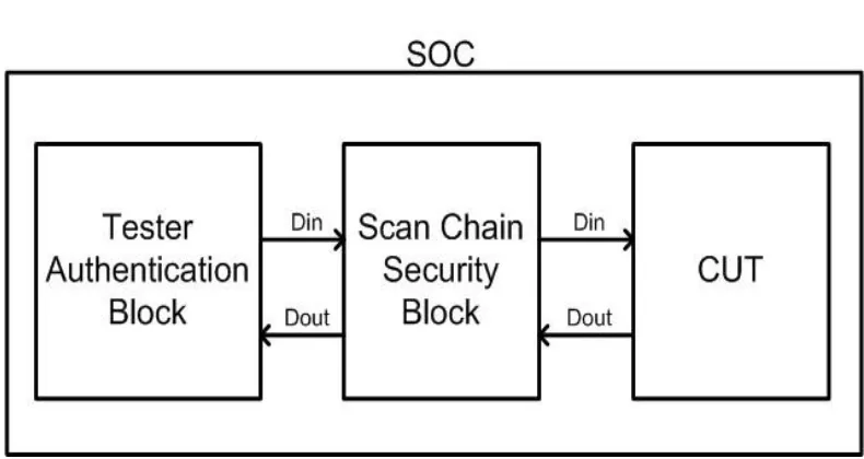
authentication and (b) scan protection. The proposed internal structure of a CUT is shown
in Figure 9. The CUT consists of a tester authentication block and a scan-chain security
block. In the proposed solution, unlike previously implemented methods, where the tester
can apply test vectors to the scan chain, the CUT requests the tester identification code
before allowing the tester to apply test vectors to the scan chain as shown in Figure 10. The
(a)
(b)
25
number of attempts for the tester authentication is limited and exceeding the maximum
number will result in denying further authentication attempts.
3.2.1 Tester Authentication Block
The steps for tester authentication by CUT are described below:
Step 1: Once the connection between the CUT and the tester is established, the CUT
applies a Clk signal to the tester to obtain the serial key from the tester through Dout as
shown in Fig. 10 (a).
Step 2: The tester receives the Clk signal and sends the serial key to the CUT as indicated
in Fig. 10 (b).
Step 3: The CUT receives the serial key and compares it with a preloaded serial key in the
authentication register.
26
Step 4: If the authentication is successful, the second layer of security is activated. Else,
the CUT sends an authentication failure message to the tester.
Step 5: When the authentication fails, the trial counter is incremented. If the count reaches
a predefined number, the pass/fail logic is disabled which in turn blocks the access to the
secure scan chain.
The authentication block in Figure 11 mainly consists of n-bit authentication register, a key
comparator, a pass/fail logic and a counter. The authentication register stores a predefined
n-bit serial key to authenticate the tester. The key comparator compares the tester key and
the authentication key and sends the result to pass/fail logic. The counter is used to
determine the number of authentication failures and blocks further authentication attempts
once a predetermined number of failures has been reached.
3.2.2 Scan based attacks
Scan chains are designed to provide access to the circuit-under test through test access port
in order to apply test data to CUT during the test mode. The responses obtained from CUT
are also captured by the scan chain for evaluation. A scan-based attack incorporates four
operations as follows:
1) Scan-in: This step is divided into two phases as well. First, test data are serially loaded
into the scan flip-flops connected to the input pins. Second, the loaded data is applied as a
test vector to the CUT.
2) Response capture: The CUT response to the applied test vector is captured by the scan
27
3) Scan-out: Shifting out the responses captured by the scan-flip to make the data available
serially at Test Data Output (TDO).
4) Response evaluation: The CUT response to the applied test vectors is analyzed to unfold
the internal circuitry and to determine the position of the secret registers.
To counter the steps involved in the scan-based attack, and make the data obtained from
scan chain many solutions have been presented in the literature. Adding random inverters
to the scan-chain [7], scrambling the scan chain [3] and using a mirror key in the test mode
[5] for cryptography are among the known solutions.
3.2.3 Secure scan chain
After tester authentication, access to the scan chain is granted and the tester can apply test
vectors to the scan chains and observe the output responses. An authenticated user can
encrypt the scan output. There are various encryption methods to prevent the use of scan
architecture by attacker. In [11] the flip-flops in a scan chain are dynamically reordered to
protect the secrets. However, the scan chain structure can be revealed by statistical analysis
of the information scanned out from chips. In [4] a lock and key security solution that is
based on a test key to secure the on-chip information is presented. This technique suffers
from the problem of large area overhead. A method proposed in [12] where a secure scan
chain architecture, based on Mirror Key Register (MKR), is used to maintain testability
and security. In this method, the encryption key is used for functional mode of operation
however; a fake mirror key is loaded in the test mode to protect the genuine key against
28
In this work to protect against the scan-based attacks, the solution presented in [12] is used
as the second layer of security for the proposed tow-layer security solution. To ensure
protection against scan-based attacks, the encryption key in [12] is generated by an array
of flip-flops. The flip-flops are hardwired to generate a private encryption key at the power
on state as shown in Fig. 4. To protect the secret code against scan-based attacks, the direct
access to the flip-flops has not been provided in the test mode. Instead, a Built-In Self-Test
(BIST) method using a Linear Feedback Shift Register (LFSR) is implemented. In the test
mode as shown in Figure 12, an LFSR is formed using the first three flip-flops in the chain
of flops. The test patterns generated by the LFSR are applied to the hardwired
flip-flops in the test mode. Using such a BIST solution for the flip-flip-flops containing the
encryption key eliminates the chance of obtaining the key through the scan architecture.
29
3.3 Implementation
Figure -14 Area overhead of the authentication block
Table 2: Area overhead measurements
32 bits of register test key
Element Size (µm x µm)
A counter 18 × 189.8
An XOR 5.8 × 6.6
A trial counter 6 × 73.8
30
The proposed solution of the tester authentication for scan chain has been implemented
with Cadence design tools using CMOS 0.18µm technology as shown in Figure 13. The
area overhead including: test key comparator, counter, 32-bits register and trial counter is
reported in table 2. The area overhead for the scan protection block depends on the number
of bits in the register and the counter. When the register test key size increases, the counter
size increases as well. The size of the test key comparator does not change with the
variations of the register test key size. The trial counter’s operation is mostly independent
of the size of the register test key, which is based on the number of attempts. For the
implementation in work, a 32-bit test key is used.
The number of bits in the test register is dependent on the degree of the complexity required
to prevent a scan chain against attacks. Increasing the size of the register test key increases
the security of scan architecture at the cost of a higher area overhead due. A large size test
key register makes a brute force attack impossible in practice. In the proposed solution, the
number of unsuccessful attempts is limited to four times. After four unsuccessful attempts,
the circuit is locked and it has to receive a power on reset to restart. This by default takes
about two seconds. Assuming a tester with a clock frequency of 2.9GHz is used to break
a 64-bit user identification key through a brute force attack, the estimated time to apply test
vectors thorough a brute force attack exceeds more than 15 years. It is assumed that each
cycle of applying an input test vector and observing the output response takes 20 clock
cycles.
The attacker may try to use a side channel attacks such as power analysis [13] timing
analysis [14], or fault injection attacks [15] [16] to obtain the critical information. To
31
the test mode. In the test mode, an attacker can apply inputs and observe corresponding
outputs. The correlation between the inputs and outputs can provide the required data to
extract the security critical information. In the proposed solution, the content of the
encryption key registers is protected against side channel attacks in the test mode.
Revealing the encryption key in the proposed solution becomes extremely difficult as the
number of bits in the register test key increases. An unauthorized tester will be able to apply
test data for one of the following cases:
• An unauthorized user must first determine the technique used to protect scan chain
• An unauthorized user has to figure out that there is a limited number of trail for
tester authentication
• If an unauthorized user figures out that there is a tester authentication, the user still
cannot access the critical security information due to the implemented BIST for the
encryption key.
The proposed solution is scalable and depending on the desired security level, the level of
the security can be determined. It is clear that a higher level of security requires more
resources and more silicon area for implementation.
3.4Comparative analysis
There is a range of solutions in the literature for security against scan-based attacks [4, 7].
The proposed approach, presents tester authentication to prevent unauthorized tester from
32
architecture using a mirror key register. The area occupied by the secure scan architecture
is 412 gates that is 1.32% of the original area.
The area overhead for implementation of Lock and Key security solution [4] on a chip is
relatively low for 4 bits (327 gates). However, increasing the number of bits to 12 bits has
a significant effect on the area overhead (5817 gates) due to the use of linear shift
registers (LFSR’s) and decoders. The proposed solution uses a minimum number of
components including resulting in an area overhead of about 2200 gate using CMOS 0.18
µm technology.
3.5Conclusion
This paper presents a new approach to protect scan architecture against attacks. The
proposed solution has two layers of security. First, the circuit-under-test identifies testers
by requesting an identification code through test access port. The tester authentication
process limits the access to the scan chain only to known testers. Once the tester is
successfully identified, it is allowed to carry out tests however, the tester still cannot
access critical security information in the circuit-under-test due to the second layer of
security. The private encryption key, which is the target for attackers, is not accessible
through the scan architecture. In the proposed solution, a built-in self-test measure is used
to test the private key generator rather than the scan architecture.
The proposed solution has been implemented using Cadence design tools in CMOS
0.18μm technology. A comparative analysis was also performed in order to evaluate the
33
3.6References
[1] D. Rolt, Jean, et al. "A smart test controller for scan chains in secure circuits."
2013 IEEE 19th International On-Line Testing Symposium (IOLTS). IEEE, 2013.
[2] D. Mukhopadhyay, S. Banerjee, D. RoyChowdhury, & B. Bhattacharya, "
CryptoScan: A secured scan chain architecture," 14th Asian Test Symposium (ATS'05)
(pp. 348-353). IEEE. (2005, December).
[3] Y. Atobe, Y. Shi, M. Yanagisawa, & N. Togawa, "Dynamically changeable
secure scan architecture against scan-based side channel attack," CUT Design Conference
(ICUTC), 2012 International (pp. 155-158). IEEE (2012, November).
[4] J. Lee, M, Tehranipoor, C, Patel, and J. Plusquellic "Securing Scan Design using
Lock and Key Technique," 20th ternational Symposium on Defect and Fault Tolerance in
VLSI Systems, 2005, pp. 51-62.
[5] B. Yang, W. Kaijie, and K. Ramesh, "Secure scan: A design-for-test architecture
for crypto chips," IEEE Transactions on Computer-Aided Design of Integrated Circuits
and Systems 25, no. 10 (2006): 2287-2293.
[6] Y. Shi, T. Nozomu, Y. Masao, and O. Tatsuo, "Robust secure scan design against
scan-based differential cryptanalysis," IEEE Transactions on Very Large Scale
Integration (VLSI) Systems 20, no. 1 (2012): 176-181.
[7] G. Sengar, D. Mukhopadhyay, and D.R. Chowdhury, "Secured Flipped
Scan-Chain Model for Crypto Architecture," IEEE Transactions on Computer-Aided design of
34
[8] M. Agrawal, S. Karmakar, D. Saha, & D. Mukhopadhyay, "Scan based side
channel attacks on stream ciphers and their counter-measures," International Conference
on Cryptology in India (pp. 226-238). Springer Berlin Heidelberg (2008, December).
[9] J. Lee, M. Tebranipoor, & J. Plusquellic, "A low-cost solution for protecting IPs
against scan-based side-channel attacks," 24th IEEE VLSI Test Symposium (pp. 6-pp).
IEEE (2006, April).
[10] D. Hely, F. Bancel, M.L. Flottes, B. Rouzeyre, "A Secure Scan Design
Methodology," in Proceedings of Design Automation and Test in Europe, 2006 , pp. 1-2.
[11] Y. Atobe, Y. Shi, M. Yanagisawa, & N. Togawa," Secure scan design with
dynamically configurable connection," Dependable Computing (PRDC), 2013 IEEE 19th
Pacific Rim International Symposium on (pp. 256-262). IEEE (2013, December).
[12] A. Mehta, D. Saif, R, Rashidzadeh, "A Hardware Security Solution against
Scan-based Attacks," unpublished.
[13] P. Kocher, J. Jaffe, and B. Jun, "Differential Power Analysis," Lecture Notes in
Computer Science, vol. 1666,pp. 388–397, 1999.
[14] J. Kelsey, B. Schneier, D. Wagner, and C. Hall, “Side Channel Cryptanalysis of
Product Ciphers," in Proc. Of the European Symposium on Research in Computer
Security, Sept. 1998, pp. 97–110.
[15] D. Boneh, R. A. Demillo, and R. J. Lipton, “On the Importance of Checking
Cryptographic Protocols for Faults,” Lecture Notes in Computer Science, vol. 1233, pp.
35
[16] E. Biham and A. Shamir, "Differential Fault Analysis of Secret Key
36
Chapter-4
Secure Scan Chain using a Phase Locking Authentication Technique
4.1 Introduction
The advent of three-dimensional integrated circuits (3D IC) brings forth a range of
possibilities through heterogeneous integration circuit integration. In 3D ICs the
conventional 2D dies are stacked to create a vertical structure. The dies that are stacked
over each other can be of different technology and can be integrated using the die to die
interconnects TSVs (Through Silicon Via) [1]. The DfT (Design for Testing) techniques
like scan architecture or BIST implemented in each level of 3D ICs serve as a gateway for
attackers to access any sensitive information stored in the 3D IC [2].
3D ICs face security threats similar to the conventional 2D ICs like scan-based attacks,
hardware Trojan, overbuilding and side channel attacks [3]. Existing security solutions and
countermeasures for 2D ICs can be integrated with 3D ICs. However, the tester may lose
controllability and observability since there is a tradeoff between security and testability.
Securing 3D ICs will restrict access to the DfT architecture, which lowers security risks
but also lowers its testability. The area overhead of 3D ICs will increase as each layer of
the 3D IC needs to be secured. There are many 3D IC architectures that utilizes scan
architecture in their DfT [4] solution. 3D ICs face the same security risk as the conventional
2D ICs that use scan architecture based DfT with access to the scan architecture. In scan
based attack, an attacker with access to the scan chain can apply input to the scan chain
37
For known scan based attacks there are two types of secure scan chain architectures which
are most commonly used [6]. The first type restricts access to the scan chain via tester
authentication with the use of a private controller. Only authorized testers are allowed to
access the scan chain. The access to the scan chain is granted only if a predetermined key
is entered [7]. In some cases, the test vectors are used as authentication keys [8].
The second type allows the tester to access the scan chain but the captured responses are
encrypted. In this method, the scan chains are modified by adding various gates and using
various encryption techniques to encrypt the output response obtained through the scan
chain. In [9] a smart test controller is introduced which masks the scanned-out responses.
In [10], inverters are randomly placed in the scan chain to make the output seem random.
It is difficult for a hacker to guess the location of the inverters, but a reset attack can reveal
the location of the inverters. When the system is reset, a stream of zeroes with ones are
obtained where the ones indicate the locations of the inverters present in the scan chain.
This paper presents a secure solution against scan-based attacks on 3D ICs. In the proposed
solution, a Phase Locked Loop (PLL) is used to authenticate the tester. The
device-under-test (DUT) includes a PLL based fractional-N synthesizer to generate an internal clock for
the scan architecture. The synthesizer generates a clock with frequency N times higher than
the frequency of a reference oscillator. The tester has to know “N” to be able to apply data
to the scan chain. Moreover, the tester has to be synchronized with the embedded
synthesizer and lock on the DUT internal clock to apply the data to the scan chain. This
method requires the tester to enter a secret code to become synchronized with the DUT to
access the scan chain as shown in Figure 14. If the tester and the DUT are not synchronized,
38
layer of a 3D IC can have its own authentication requirement. The proposed method
provides security to scan architectures in all layers. The tester needs to synchronize with
the DUT to access the scan chain in each layer. The hardware synchronization requirement
reduces the security threats using a brute force attack. The area overhead remains the same
irrespective of the number of layers in the 3D IC.
The rest of the paper is organized as follows: section II explains how the scan attacks work;
section III discusses the proposed solution for 3D ICs security threat; section IV provides
implementation and simulation results; section V compares the proposed method with
existing methods and conclusion in section VI.
Figure -15 The frequency matching process involving PLL.
DUT Scan Flip Flop 1 Scan Flip Flop 2 Scan Flip Flop N
PLL Based Frequency Synthesizer
Oscillator Synthesized
Clock(Nfref)
39
4.2 Scan Based Attack:
The process for a scan-based attack is described below:
1) Scan in: The test vectors are shifted in serially through the test access port into the
scan flip-flops connected to the input pins of the device and applied to the DUT inputs.
2) Capture response: The DUT’s response to the test vectors are captured by the scan
flip-flops.
3) Scan out: The captured responses are shifted out serially at the test port.
4) Response evaluation: The scanned-out output is then evaluated to determine the
internal circuitry or the encryption key used.
Figure -16 Components of DUT.
Phase Locked Loop
Scan Chain
Security Block CUT
Dout Din DUT
40
4.3 Proposed Solution For Secure Scan Architecture In 3D-IC
The proposed method involves a PLL used to authenticate the tester and support a secure
scan architecture as shown in Figure 15. In this method, the DUT initiates the
authentication process rather than the tester. In the DUT, an oscillator generates a reference
clock signal, fref . The clock signal is fed into the divide by N PLL based synthesizer to
generate an internal clock signal (Nfref) for the scan architecture. N is a secret code for
the Frequency Divider in the PLL. The reference clock signal, fref , is applied to the tester
through the TCK pin of the Test Access Port (TAP). The tester uses its own divide by N
synthesizer to lock on the applied clock signal to generate an internal clock signal(Nfref )
synchronized with the internal clock of the DUT. After the tester clock become
synchronized with the DUT internal clock, it can properly access the scan chain and apply
the test vectors to the DUT and capture the responses. The tester cannot synchronize its
operation with the internal clock of the DUT without the knowing the value of “N”.
This solution provides an advantage of securing 3D ICs by utilizing the phase locking
technique. Conventional security measures used for scan architecture in 2D ICs can be
integrated into 3D ICs. However, in this case each layer of scan architecture will require
its own security increasing the area overhead and the complexity. The proposed method
serves as a single authentication method for the entire 3D IC. This solution can be further
developed by assigning different N value to different layers in the stacked ICs. Thus, each
layer will require a unique synchronization requirement between the tester and the DUT.
The tester must know the secret code, N, for each layer of 3D IC to perform the test.
41
the output response obtained will be random and inconclusive. This method also has a
secure scan architecture, which prevents the tester from accessing the sensitive information
stored in the DUT [13].
4.3.1 Phase Locked Loop (PLL)
The PLL block in Figure 16 consists of a Phase Frequency Detector, a charge pump,
Voltage Controlled Oscillator (VCO) and a Frequency Divider (N-Divider) [11]. The
divide by N frequency divider used in the PLL can be replaced with a fractional divider
(M/N Divider) for higher security.
The process involved in synthesizing internal clock frequency for both tester and the DUT
using PLL is described below:
Step 1: The Frequency Phase Detector compares the clock frequency and the N- divided
feedback frequency and produces a voltage proportional to their phase difference.
Step 2: The output voltage of the Frequency Phase Detector is then fed into the Charge
Pump where a control voltage is produced and applied to a Low Pass Filter.
Step 3: The filtered control voltage drives the Voltage Controlled Oscillator (VCO) made
up of a ring oscillator is used to create a signal with a frequency proportional to the input
clock frequency.
Step 4: The output is then fed to a frequency divider, which divides the VCO signal, by an
integer N and looped back to the Frequency Phase Detector. Depending on the value of the
integer N, the PLL generates a clock signal with frequency that is relative to the input clock
42
4.3.2 Secure scan chain
Once the PLL inside the tester locks on the clock signal supplied by the DUT, it can apply
the data to the scan chain. However, the tester still cannot access the internal circuit of the
DUT due to the second layer of security.
The second phase of the proposed method uses the solution proposed in [13] in
which an array of flip-flops is utilized to generate an encryption key at power on state as
shown in Fig. 4. This method utilizes the Mirror Key Register (MKR) where the encryption
key is utilized during the normal functional mode however during the test mode; a fake key
is loaded into the register to protect the encryption key from the tester. A linear Feedback
Shift Register(LFSR) based Built-In-Self-Test(BIST) is implemented to restrict access to
the scan chain. The LFSR is formed using the first three flip-flops of the scan chain as
shown in Figure 17 The test patterns generated by the LFSR are applied to the hardwired
flip-flops in the test mode. This method protects the encryption key against a scan chain
based attack.
Figure -17 PLL Block Diagram.
Charge Pump And Low Pass
![Figure -9 Boundary Scan Architecture [7].](https://thumb-us.123doks.com/thumbv2/123dok_us/1377666.1170450/34.612.111.542.78.524/figure-boundary-scan-architecture.webp)