ABSTRACT
KOMMAJOSHYULA, PRADYUMN. Experimental Study of Nano Electro Machining. (Under the direction Dr. Paul Cohen.)
Scanning Probe Lithography (SPL) is one of the methods used for synthesizing
nano-structured materials and devices. SPL potentially 3D, relatively fast and needs no expensive
masks. Nano milling and nano electro machining are recent developments in SPL. Nano
electro machining is analogous to electric discharge machining which removes material by
discharge between two electrodes (work piece and tool). The nano-scale version involves
Atomic Force Microscope (AFM) tip and sample act as electrodes. Previous works
removed material by adding negative pulses to AFM tip. These attempts resulted in hole
with diameters typically spanning around 100 nm in width or diameter and 50 nm in depth.
Some environments in which nano electro machining was done include air and dielectric
oil. Some sample materials include Highly Ordered pyrolitic Graphite (HOPG), gold,
copper. Here an experimental study of the process parameters of the nano electro
machining is done using HOPG. The process parameters peak to peak voltage of the pulse
and number of pulses or time of machining are studied using factorial experiments by
fabricating holes with several combinations of these parameters. Out of these two
parameters peak to peak voltage or simply voltage was found have a much greater impact
on the material removed on the HOPG work-piece. Further fabrication of trenches or slots
was also found to be feasible. In addition nano electro machining HOPG using a
Finally the dimensions of holes made by the nanowire and standard tip were compared and
Experimental Study of Nano Electro Machining
by
Pradyumn Kommajoshyula
A thesis submitted to the Graduate Faculty of North Carolina State University
in partial fulfillment of the requirements for the Degree of
Master of Science
Industrial Engineering
Raleigh, North Carolina
2013
APPROVED BY:
__________________________ ________________________ Dr. Ronald Scattergood Dr. Jingyan Dong
____________________________ Dr. Paul Cohen
ii
BIOGRAPHY
Pradyumn Kommajoshyula was born in Chennai, India on April 30th 1989. He
completed the greater part of his school education there and finished high school in Boston
School, Chennai, India. In 2006, he began college at Velammal Engineering College,
under the umbrella of Anna University, majoring in Mechanical Engineering. He
enrolled for the Master of Science program in 2010 at North Carolina State University,
iii
ACKNOWLEDGMENTS
I would first like to thank my advisors, Dr. Paul Cohen and Dr. Jingyan Dong for all
of t heir guidance and support, during the research. I also want to thank Dr. Ron
Scattergood for being a committee member, as well as for his guidance. I am indebted to
Li Zhang for all his assistance without which this would not have been possible. I
also thank all the other students in Dr. Cohen and Dr. Dong’s group for their assistance.
Finally, I would like to thank my family and friends for their support throughout my
iv
TABLE OF CONTENTS
LIST OF TABLES ... vi
LIST OF FIGURES ...x
1. INTRODUCTION ...1
2. LITERATURE REVIEW ...3
2.1 Scanning Probe Lithography ...3
2.2 Mechanical Scratching and Nano-milling ...3
2.3 Oxidation and Scanning Tunneling Lithography ...4
2.4 Nano Electro Machining ...5
3. EXPERIMENTS ...8
3.1 Equipment and Setup ...8
3.2 Outline of the Experiments ...11
4. RESULTS AND DISCUSSION ...15
4.1 Study of the Resulting Hole Dimensions Made by a Wide Range of Voltages ...15
4.1.1 Variation of the Resulting Hole Dimensions Made by a Wide Range of Voltages ...16
4.2 Study of Repeatability ...19
4.2.1 Characterization of Repeatability ...20
4.3 Investigation of Voltage and Pulses on the Dimensions ...22
4.3.1 Influence of Voltage and Pulses on the Dimensions and Repeatability ...23
4.4 Fabrication of Slots ...31
4.4.1 Dependence of Slot Dimensions on the Input Parameters ...31
v
4.6 Explanation of Different Hole Shapes Arising due to Different Tip Geometries...38
4.7 Comparison with Other Results ...46
5. CONCLUSION AND FUTURE WORK ...50
6. REFERENCES ...53
7. APPENDIX ...57
A. Additional Results from HOPG Experiments ...58
B. Additional Images from the HOPG Experiments ...68
C. Images from the HOPG experiments ...74
D. SEM Images Showing Tip Wear ...77
E. Derivation of the Transmission Coefficient for F.N. Tunneling ...82
vi
LIST OF TABLES
Table I The parameters used in all experiments on HOPG. ...12
Table II Parameters used in experiments with the standard tip. ...16
Table III ANOVA of the 3x3 factorial experiment with 7V, 6V and 5 V and 4,8 and 12 pulses. ...27
Table IV Input parameters used in making each slot. ...32
Table V Experimental data showing the differences in the dimension of holes made by two tips of different aspect ratios with same voltage and number of pulses. The sample was HOPG. ...38
Table VI Various material removal rates for various experiments. ...47
Table VII A statistical model for the 7V, 6V and 5 V and 4,8,12 experiment ,repeated four times, with depth as the output variable ‘Y’. (‘X variable 1’ is ln(PV) and ‘X variable 2’ is ln(P)). ...63
vii
LIST OF FIGURES
Figure 1 Schematic experimental setup of the system. ... 9
Figure 2 Conductive epoxy to the chip carrier plate. ... 11
Figure 3 (a) AFM image of a 12x3 factorial experiment done with 9.5 V to 4 V (from left to right) in steps of 0.5 V and 1,2,4 (top, middle and bottom row in that order) taken in non-contact mode (b) is the profilometer image. ... 17
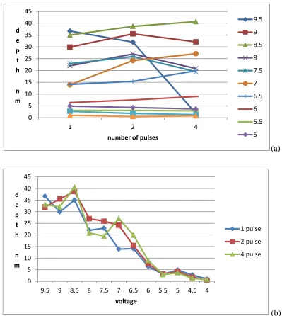
Figure 4 (a) Plots of depth vs. number of pulses for each voltage and (b) depth vs. voltage for each. ... 18
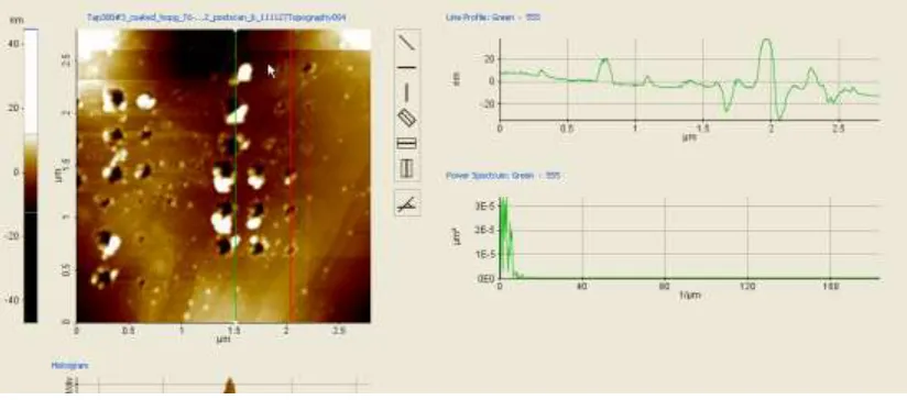
Figure 5 AFM image of four 3x3 arrays on the left hand side. Each array consists of 9 holes made in a factorial experiment with 7 V, 6 V and 5 V (in that order) and 1,4 and 8 pulses. The green line indicates the cross-Section of some of the holes that is found in the right hand side of the figure. ... 21
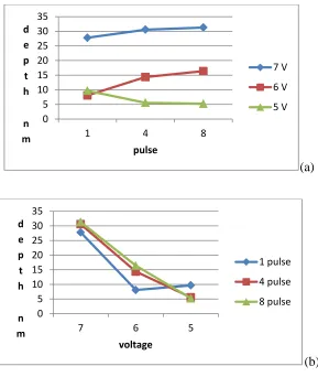
Figure 6 (a) Plots of average depth vs. number of pulses for each voltage and (b) of average depth vs. voltage for each pulse. ... 22
Figure 7 Left hand side is the AFM image of a 3x3 array made in factorial experiment. The input number of pulses increase in steps of 4,8 and12 with each hole from left to right. The input voltage increases in steps of 7 V, 6 V and 5 V in that order, with each hole from top to bottom. Right hand side depicts the cross Section of some of the holes corresponding to the red line on the L.H.S. ... 23
Figure 8 (a) Plots of average depth vs. number of pulses for each voltage and (b) plot of average depth vs. voltage for each pulse. ... 25
Figure 9 Shows the range (difference between maximum and minimum values) of width of holes in the factorial experiment involving 7 V ,6 V & 5 V and 4,8 &12 pulses repeated four times against the voltage. ... 30
Figure 10 Shows the range (difference between maximum and minimum values) of depth of holes in the factorial experiment involving 7 V ,6 V & 5 V and 4,8 &12 pulses repeated four times against the voltage. ... 30
Figure 11 AFM image of a slot of 8 holes made by 6 V and 4 pulses each. The other slot is made by 6 V and 8 pulses. ... 33
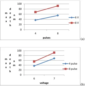
Figure 12 (a) Plots of max depth vs. number of pulses for each voltage and (b) plot of max depth vs. voltage for each pulse. ... 34
viii
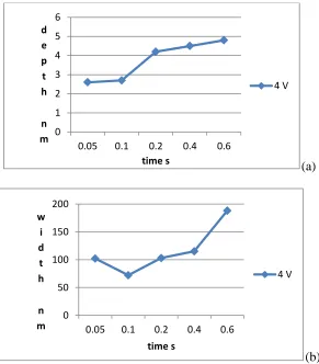
Figure 14 (a) Plot of width(diameter) of the resulting hole when using the nanowire against number of pulses for 4 V. (b) Plot of depth of the resulting hole when using the nanowire against number of pulses for 4 V. ... 37
Figure 15 (a)The schematic representation of the trends of the distribution of the squared transmission coefficient. For the sharper tip the distribution on the flat surface broadens (depicted more clearly in Figure 15). The y-axis is the transmission coefficient and the x-axis can be thought of as the same surface relative to the location of the tip. (b)The distribution of squared transmission coefficients of the standard tip (red) and nanowire (blue) are plotted in the same graph. The x-axis represents the location on the flat sample surface. The origin represents the point directly underneath the center of the tip. ... 44
Figure 16 The average width dependence for an experiment done with 7 V, 6V and 5 V and 1,4 and 8 pulses on (a) pulse for each voltage and (b) voltage for each pulse. ... 58
Figure 17 The average width dependence for an experiment done with 7 V, 6V and 5 V and 4,8 and 12 pulses on (a) pulse for each voltage and (b) voltage for each pulse. ... 59
Figure 18 The width dependence for an 12x3 experiment done with 1,2,4 pulses and voltage decrease from 9.5 to 4 V in steps of 0.5 V on (a) pulse for each voltage, x-axis is number of pulses and (b) voltage for each pulse x-axis is voltage. ... 60
Figure 19 (a) Depth dependence on pulse for each voltage for all four times repeated and (b) width dependence on pulse for each voltage for all four times repeated for a 3x3 experiment with 7V,6V and 5V and 4,8,12 pulses. ... 62
Figure 20 The plot shows the volume of material removal removed (assuming the holes are cones) against the number of pulses or machined time. Y-axis is in 1000 cu. Nm. The x-axis is in seconds. The slope of the curve would give the material removal rate for each voltage. ... 65
Figure 21 (a) Depth in nm and (b) width in nm of the holes made by the nanowire in a 3x3 experiment that depends on voltage for each pulse. The decrease in dimension towards the end may attribute to the gradual wearing of the nanowire which stopped working just after this experiment. ... 66
Figure 22 Width dependence of the slot on the parameters in a 2x2 experiment on (a) pulse for each voltage and (b) voltage for each pulse. ... 67
ix
varies as described in the figure. (b) AFM image of the same experiment. Each of the colored boxes corresponds to the box in Figure 24 (a) which gives the sequencing of machining of each hole within an experiment. ... 69
Figure 24 (a) 3D image of the 3x3 experiment. There are 3x3 four matrices each made by combinations of 5V, 6 V and 7 V and 1,4 and 8 pulses. (b) Inverted image of the 3x3 factorial experiments shown in Figure 24 (a) to show clearly the dimensions of holes. ... 70
Figure 25 Four holes fabricated using the nanowire with 4 V. There is one hole at each corner of the box. As depicted in Section 4.5 and Section 4.6 the holes made by the nanowire are shallow (slightly higher in depth and much larger in diameter/width) than those made by standard tip. ... 71
Figure 26 A successfully fabricated slot using 6 V which has the ‘best’ step-over distance between each hole. The top holes show a failed attempt as the step-over distance between the holes was too large. ... 72
Figure 27 (a) A 12x3 factorial experiment. Holes are fabricated with varying voltage from 9.5 V to 4 V in steps of 0.5 V. This structure resembles a quantum anti-dot array. (b) The inverted image of the same 12x3 experiment shown to illustrate the variation hole depth and diameter with voltage. ... 73
Figure 28 (a) A slot fabricated on aluminum by nano electro machining using -9.8 V (b) 3D image of the same trench or slot. . ... 75
Figure 29 (a) AFM image of another slot on aluminum made by -9 V. (b) 3D image of the aluminum trench made by -9 V. It is not as conspicuous as the one in Figure 28 because the tip was on the verge of completely wearing out and the roughness of the sample. ... 76
Figure 30 (a) SEM image of a typical brand new silicon tip coated with gold. (tip was pre-coated by the manufacturer; tip was a Ktek tetra-16 Au) (b) And SEM image of the same tip after nano electro machining multiple times with voltages up to 8 V. ... 77
Figure 31 (a) SEM image of a polycrystalline Ag nanowire tip around 3 to 4 um in length attached to a standard tip (b) Magnification of the mentioned tip shows that the very tip is curved (c) The red circle profiles the tip as a hemisphere with 200 nm diameter. ... 79
x
Figure 33 (a) SEM image of a standard tip before attaching a nanowire. This tip represents the profile of a typical standard tip before nano electro machining. (b) Magnification of the mentioned tip shows that the very tip is curved (c) The red circle profiles the tip as a hemisphere with 200 nm diameter. The standard tips that were used for nano electro machining were used previously used extensively as a mechanical ploughing tool on polymer films for a different project. ... 81
Figure 34 Schematic representation of the two types of tunneling. ... 82
Figure 35 Potential between two materials (region 0 and l) with uniform electric field.. 84
Figure 36 Approximation of the potential from smooth line to piece-wise potential. ... 85
Figure 37 The approximated potential. The stepwise region has N segments. ... 85
1
1. INTRODUCTION
Increasing demands of the electronics sector is pushing the semiconductor industry
into reducing the size of transistors, photodiodes, emitters and sensors from micro-scale to
nano-scale. The advantage of nano-scale features is not just the obvious size advantage but
also exploiting quantum effects [1]. Fabrication of devices in the nano-scale involves
several choices of processes like etching [2] and deposition [3] which is top-down and
bottom-up respectively. However there are several devices that need to be selectively
etched or deposited in order to fabricate them. Most of these involve slots trenches or
holes. The fundamental limit of photo-lithography is light itself. The resolution of the
nano-scale features are limited by the wavelength of light. Thus these smaller patterns are made
by other means with scanning probe lithography being one of them. Electron beam
lithography [4] which can easily fabricate these features places many constraints on the
equipment used because of the requirement of vacuum. Scanning probe lithography
facilitates relatively simple handling of equipment. There are many forms of scanning
probe techniques some are the oxidation and mechanical scratching using an atomic force
microscope. The other is the scanning tunneling microscope lithography. A relatively new
type of lithography is the spark erosion, “electric pen” or the nano electro machining. This
has several advantages over the other processes which are briefly discussed in the next
section. Potential applications include plasmonic LEDs [5] and the quantum anti-dot arrays
2
lithographically resembles a quantum anti-dot array. In this thesis the process parametrical
3
2. LITERATURE REVIEW
2.1 Scanning Probe Lithography
The atomic force microscope was primarily built for imaging surfaces of materials [7]
or for imaging the nano-scale patterns fabricated on the material [8]. The AFM can be used
to measure electrical properties [9], magnetic properties [10] or measuring surface topology
[11]. However, the atomic force microscope has also been used to fabricate nano-scale
patterns. Most of these involve the tip removing material [12] [13] [14] and others build up
or change the composition of the material [15] [16]. Usually this method of fabrication
produces patterns in the form of holes or trenches [17]. In many cases this is not the final
product or device and further processing is needed. In case of mechanical scratching the
photo-resist needs to be removed after etching the material underneath.
2.2. Mechanical Scratching and Nano-milling
In this form of lithography the tip approaches the surface, indents it and is moved to
form a pattern. The tip can be move to plough the material to make nano-scale slots [18].
However due to the nature of the process it is almost always limited to soft materials
although there were exceptional cases [19]. This leads to making patterns only on soft
polymers like photo-resists deposited on a substrate material and then further processed to
make the desired device [20]. Using this method the AFM tip is used to make nano-scale
trenches on the photo-resist which is deposited on the substrate thus exposing the substrate
4
micro or nano-sensor or an actuator [21]. There are several improvements to this process to
remove more material including vibrating the sample on a custom made z-stage [22]. A
hardened diamond-like carbon tip can remove a large volume of material by vibrating the
stage x and y direction and may be even in the z direction [22]. This simulates the milling
machining operation in machine shop.
2.3. Oxidation and Scanning Tunneling Lithography
Another lithography process involves patterning by means of electrical contact. The tip
is approached to the surface and instead of mechanically ploughing or scratching; an
electric field is applied between the tip and surface. This electric field causes some
manipulation on the surface. The surface features formed are in most cases oxides of the
work-piece material. The electric field can be direct current or a pulse. This electric field
induced oxidation [23] can be used for further processing, making the desired devices. The
areas where the AFM tip enabled oxidation produce a different reaction to etching agents
[25]. This can be used to make patterns as the etching material removes material around the
oxidized regions. The second kind of manipulation is scanning tunneling lithography.
Scanning tunneling microscopy is used to map the surface topology of a material by
measuring the tunneling current between the tip and the sample while scanning [25]. The
STM can also be used for patterning as a chemical reaction by the free charges of the
5 2.4 Nano Electro Machining
A new kind of lithography performed by means of applying basically an electrical pulse
to sample via the AFM tip is the nano electro machining. Nano electro machining is
analogous to the electric discharge machining at the macro scale. Electric discharge
machining or spark erosion is a non-traditional machining process at the macro scale. This
involves material removal by means of spark erosion between the tip which acts as the
electrode and the conducting sample in presence of a dielectric medium. This process has
also been replicated in the micro-scale [28 to 30] in which pulses (hundreds of
microseconds in periods) are applied between a tool (ex: Tungsten and 50 um diameter)
and a conducting work piece in presence of a hydrocarbon based dielectric. The electric
discharge between the tool and work-piece creates in holes of around 100 um in diameter.
The material is eroded by the thermal energy that results from the discharge [29].
The nano-scale version is performed by treating AFM tip (as opposed to the micro
fabricated and cylindrical tool in micro EDM) and sample surface as electrodes and
applying a pulse in between. The tip is given the negative pulse and the sample which is
grounded and gets eroded. The mechanism of material removal in the nano electro
machining is not known although; a previous publication ruled out some of the possible
mechanisms such as electro-migration [31]. This process has some advantages over the
processes previously mentioned. As this is direct fabrication, further process is not needed.
It can be only performed on conducting materials. However the patterns are directly
6
removal of photo-resist etc. Most of the experiments done here required no special
modifications of the AFM system other than the coating of the cantilever (40 to 60 nm of
gold and palladium by sputtering) only to make it conductive.
As the mechanism is still not completely clear, here the dependence on several
parameters of the width of the geometries and dimensions of eroded areas are explored by
means of design of statistical experiments. Many of the previous works were performed
with the medium between the tool and the work-piece being dielectric oil [32, 33]. Also
these were performed on a system designed for scanning tunneling microscopy and hence
the precise measurement of distance between the tip and substrate was possible. This
facilitated the measurement of I-V characteristics and Paschen curves which provided a
deeper understanding of the nano electro machining process. In one experiment, a tungsten
electrode was used on a gold sample showed formation of tungsten carbide and oxide
precipitates in a nano-crystalline form. This carbide formation enhanced the nano electro
machining capability. It was hypothesized that the mechanism was because of the dielectric
breakdown with some contribution of tunneling electrons. The tool after nano electro
machining had a smaller radius than the original electric field assisted nucleation of
nano-crystalline tungsten oxide and carbide phases on tool surface and sub-surface was observed.
In another study the tip was coated with Ir-Pt and performed on <111> gold under
dielectric oil. The material removal rate was 141 cu. nm/second. The authors have
demonstrated nanometer scale material removal as small as 10 nm in diameter and under 1
nm in depth. Another study was done on highly ordered pyrolytic graphite (HOPG) without
7
standard tip. The equipment used there was a scanning tunneling microscope and had
feature to precisely measure tip-surface distances and I-V characteristics. It was
hypothesized that the possible removal mechanism was that tunneling electrons induced
chemical reaction. The I-V characteristics showed that the nano electro machining
mechanism was influenced the maximum by voltage and not current. In this study, a
comparison between voltage and time of machining was thoroughly investigated. Due to
equipment restrictions it was not possible to measure the I-V characteristics nor accurately
8
3. EXPERIMENTS
3.1 Equipment and Setup
The experiments were conducted using a Park Systems XE-70 Atomic Force
Microscope. This is a standard AFM which scans images by the XYZ scanner and a
micro-cantilever. It is placed on a Minus K vibration stabilizer and enclosed in an acoustic
chamber. The AFM tips used for this experiment are the following:
1. Park Systems NCHR (stiffness: 40 N/m , radius: <30 nm, mode: non-contact)
2. Nanoandmore Tap300 (stiffness: 40 N/m , radius: <30 nm, mode: non-contact)
3. Ktek Tetra-16(Au) 40 N/m (stiffness: 40 N/m , radius: 50 nm, mode: non-contact)
For all the experiments the first two tips were coated with approximately a total
thickness of 40 nm to 60 nm of gold and palladium by sputtering to make them conductive.
The equipment for pre-coating SEM samples, at NCSU analytical instruments facilities
(JEOL 6400F), was used to coat these tips. The coating increases the tip radius, so the
actual tip radius is higher than the one specified above and depends on the coating
thickness. The third tip was already coated with gold and titanium (total thickness of 40
nm) by the manufacturer.
One of the samples used was aluminum film. This sample was prepared by thermally
depositing aluminum on silicon <100> wafers with a thickness of about 100 nm. The other
was a 10 x 10 x 3 mm highly ordered pyrolithic graphite (HOPG). The samples were
9
conductivity, is then grounded using a wire attached to the AFM ground. Two electrical
sources were used. One was a Keithley source meter was used for DC source while the
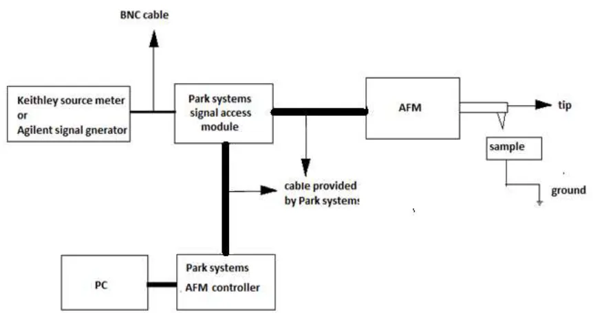
Agilent signal generator was used for pulsed signals. The ‘signal access module’ provided
by Park Systems was a box with BNC ports connecting to various systems of the AFM
including tip bias, sample bias, various imaging signal I/O etc. This access module can be
used to send custom signals into the AFM for various purposes. In this setup we send the
custom electric pulse into the AFM via the access module. The BNC from the Agilent or
the Keithley source meter is directly connected to the ‘tip bias’ port of the signal access
module. This setup ensures that the signal from the signal generator directly goes to the
AFM cantilever. Figure 1 shows a schematic of the setup.
10
All of the entities in Figure 1 except ‘Keithley source meter..’ and the ‘ground’ are
provided by Park Systems and from the normal setup. Connecting a BNC from the Agilent
to the ‘tip bias’ port of the signal access module sends the signal directly to the tip. Any
wire attached securely to the sample and the ground forms the only addition to the normal
setup of AFM in order to perform this experiment.
In addition to these two connections a conductive epoxy can be added to the ‘chip
carrier’ plate which contains the AFM cantilever which attached to the z-stage. This
ensures that the cantilever receives the signal as illustrated in Figure 2. The chip carrier
plate is attached to the z-stage and holds the chip and cantilever and it is shown in the
Figure 2. The chip carrier plate is attached to the z-stage and holds the chip and cantilever
with, conductive epoxy. All of the experiments except in case of aluminum used the
Agilent signal generator. To perform nano electro machining in case of HOPG sample the
tip must be approached to the sample and held stationary. XEL is a software package
provided by Park Systems which is used for performing lithography using the AFM. XEL
provided by Park Systems can be used to place the tip exactly at the spot desired and a
pulse can be sent to it. The Agilent signal generator allows the user to control the number
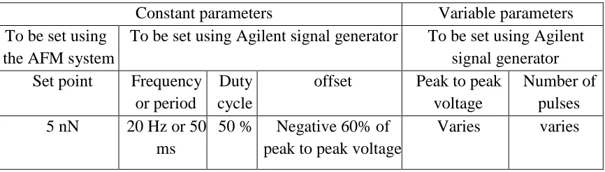
of pulses, peak-to-peak voltage, frequency etc. In case of HOPG sample the pulse, nature
and details are given in Table I. Peak-to peak voltage or simply voltage and the number of
11
Figure 2 Conductive epoxy to the chip carrier plate.
The aluminum sample was used only to check whether the AFM system with the current
setup is capable of performing lithography using this process before using the HOPG
sample. Details of aluminum sample and the experiment made using it are given in
Appendix D.
3.2Outline of the Experiments
. The aim of the experiments is to determine the dependence of dimensions of the
resulting holes on the input parameters. As observed in Table I many parameters can be
altered. In this work only two parameters were altered: the peak-to-peak voltage and the
number of pulses. From this point on the term voltage will refer to the peak-to-peak voltage
as a short hand notation. The other parameters such as duty cycle, frequency etc., are held
constant throughout this work, unless otherwise explicitly stated.
The first experiment was exploratory in nature. The experiment consists of a wide range
of voltages and a limited range of pulses. The next two experiments were performed to
12
nano electro machining becomes repeatable. The other one was to quantify the repeatability
over a large range of number of pulses.
Table I The parameters used in all experiments on HOPG
Constant parameters Variable parameters
To be set using the AFM system
To be set using Agilent signal generator To be set using Agilent signal generator Set point Frequency
or period
Duty cycle
offset Peak to peak voltage
Number of pulses 5 nN 20 Hz or 50
ms
50 % Negative 60% of peak to peak voltage
Varies varies
To examine the dependence of dimensions of the resulting hole on the input parameters,
an nxn (for some integer n) factorial experiment was performed with voltage and number of
pulses as the factors. The method is to make a single hole by applying a number of pulses
with some voltage and then fabricate more holes each with an increased voltage (all with
the same number of pulses). The next iteration would be to fabricate the same number of
holes with the same incremental voltage, but each of them with an increased number of
pulses than the previous iteration. More iterations can be performed each with increased
number of pulses. The order in which the iterations were performed may differ with each
experiment. For example, an nxn matrix of holes on the HOPG sample corresponds to an
nxn factorial experiment with voltage and the number of pulses.
13
1. Exploring all the range of voltages and small range of pulses
2. Exploring threshold voltage at which the process becomes consistent
3. Quantifying repeatability over a larger range of pulses
In addition to the experiments described above two additional experiments were performed.
One of these is to fabricate a feature on the sample other than a hole; a trench. The other
experiment is a factorial experiment similar to the one described above, with the only
difference being that the aspect ratio of the AFM tip is much lower.
The experimental procedure for these experiments is described below.
The sample used here is 10x10x3 mm highly ordered pyrolitic graphite. The sample is
hence chosen because of its high atomic flatness. As explained in the previous Section, the
sample is placed on the standard sample holder and a wire connects it to the ground. In a
typical experiment the tip is approached to the sample surface and it is held stationary and
given a voltage. The tips used were old tips which were used for some mechanical
scratching experiments. Each tip was coated with palladium and gold of around 40 to 60
nm total thickness.
In addition to the above experiment, a separate study was conducted, the purpose of
which was to test the feasibility of performing nano electro machining by attaching a
nanowire to a standard AFM tip. The nanowire (made of polycrystalline silver) is attached
by a standard AFM tip by means of an epoxy. The nanowire is estimated to have a diameter
14
the AFM tip by means of a non-conducting epoxy, the AFM tip along with the nanowire is
coated with gold and palladium with a combined thickness of 40 to 60 nm in the same
manner mentioned in the beginning of Section 3.1. The tip with the nanowire is mounted
on the AFM and the procedure used for nano electro machining is the same as the one
15
4. RESULTS AND DISCUSSION
When material was removed by nano electro machining the pattern left on the substrate
resembles a cone, similar to the cross Section of the AFM tip. Therefore the features have
two measureable parameters, height and diameter of the cone which are the diameter and
height of the cone. In case of trenches or series of holes the pattern formed was in the form
a V-shaped groove and the results were characterized in terms of width and depth of the
groove. The following Sections show the variations of the dimensions of the features using
factorial experiments for the three scenarios: holes using a standard tip, trenches or slots or
series of holes using standard tip and stray holes using a nanowire tip.
4.1 Study of the Resulting Hole Dimensions made by a Wide Range of Voltages
The aim of the following experiment was to examine the dimensions of the resulting
hole and how they depend on a large range of voltage and relatively small size of the holes.
To examine the dependence of dimensions of the resulting hole an 12x3 factorial
experiment was performed with voltage and number of pulses as the factors.
Experimentally, this 12x3 factorial experiment translates into a matrix of holes with three
rows and twelve columns on the HOPG surface. Each row contains twelve holes each made
with a different voltage and constant number of pulses. The voltage is in a decreasing order
from 9.5 V to 4 V with 0.5V as an interval. Each column contains holes made by an
increasing number of pulses 1, 4 and 8. The last column was given a voltage of 7 V and
16
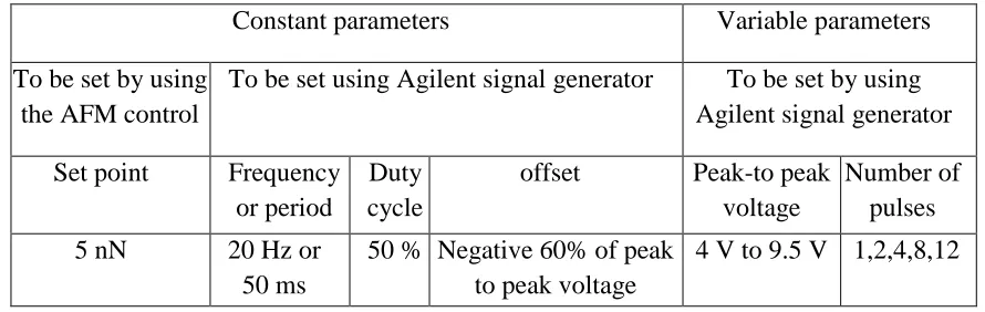
of the tip or some chronological phenomenon. Table II shows the parameters used
throughout this experiment.
Table II Parameters used in experiments with the standard tip
Constant parameters Variable parameters
To be set by using the AFM control
To be set using Agilent signal generator To be set by using Agilent signal generator
Set point Frequency or period
Duty cycle
offset Peak-to peak voltage
Number of pulses
5 nN 20 Hz or
50 ms
50 % Negative 60% of peak to peak voltage
4 V to 9.5 V 1,2,4,8,12
4.1.1. Variation of the Resulting Hole Dimensions made by a Wide Range of
Voltages
When the AFM tip is placed above the substrate and given a pulse of sufficient voltage,
material was removed and a hole was formed. The dimension of the hole, resembling a
cone, showed a dependence on the voltage and the number of pulses. A non-contact mode
image of the sample after the experiment measured the dimensions (depth and diameter) of
the holes formed. Figure 4(a) and (b) graph depth as a function of voltage and pulses. It is
clear that the width (diameter) and depth decrease with decreasing voltage and also
increase with increasing pulses. Additional results can be found in the Appendix A. The
17
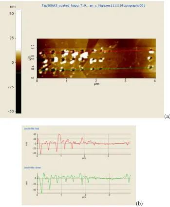
when the voltage is lower. Also the last 3 holes in Figure 3 (a) were made by 7 V and were
made after fabricating the 33 holes made from 9.5 V to 4 V.
(a)
(b)
Figure 3 (a) AFM image of a 12x3 factorial experiment done with 9.5 V to 4 V (from left to right) in steps of 0.5 V and 1,2,4 (top, middle and bottom row in that order) taken in
18
(a)
(b)
Figure 4 (a) Plots of depth vs. number of pulses for each voltage and (b) depth vs. voltage for each pulse.
This illustrates that the decrease in hole size is not a chronological phenomenon such as
tip wear and the hole diameter and depth depend strongly on voltage.
0 5 10 15 20 25 30 35 40 45
1 2 4
d e p t h n m
number of pulses
9.5 9 8.5 8 7.5 7 6.5 6 5.5 5 0 5 10 15 20 25 30 35 40 45
9.5 9 8.5 8 7.5 7 6.5 6 5.5 5 4.5 4
19
The number of pulses, however, seemingly has relatively less influence on the
dimensions of the holes. This may be because the melting of the tip material may have
resulted in debris that is deposited on the sample. This is investigated more thoroughly in
the next experiment in subsequent Sections. By this, one can concur that nano electro
machining occurs at a wide range of voltages from 9.5 V to 4 V (and beyond) and 4V is the
threshold of nano electro machining. The hole diameter and depth strongly depends on the
voltage. The next step is to quantify the dependence of voltage and number of pulses and
the repeatability.
4.2Study of Repeatability
It was established by the previous experiment that the threshold voltage for nano electro
machining is 4 V. However, it is found that the process is not very repeatable for low
voltages. Attempts to make holes with 4 V to 5 V had a low success rate i,e no material
removal was observed in many attempts. In this regard, there was a need to establish a
‘threshold’ for the minimum voltage that produced some feature on the sample every time.
The aim of the following experiment was to characterize the repeatability of the process.
To determine the repeatability threshold voltage the following experiment was performed.
The range of voltage in the experiment was small: 7 V, 6 V and 5 V. The number of pulses
in the experiment were 1, 4 and 8. The experiment was a 3x3 factorial experiment was
performed similar to the one described in the previous Section. But here, it is needed to
determine the threshold voltage for repeatability; hence this factorial experiment was
20 4.2.1 Characterization of Repeatability
The factorial experiment performed with a small range of voltage ranging 7 V, 6 V and 5
V and 1, 4 and 8 pulses revealed the repeatability threshold as 5 V. All holes made by 5 V
produced some features. The factorial experiment is a 3x3 experiment with each hole made
by a different voltage: 7V, 6 V, 5 V and number of pulses: 1, 4, 8. This experiment was
performed four times to investigate repeatability and also to explore the minimum voltage
threshold at which it is possible to repeat the experiment. This experiment also reveals that
at voltages around 5 V the size of the hole depends on the state of the tip prior to nano
electro machining. Figure 5 below shows AFM image of the 3x3 arrays. It can be noted that
the order in which they were fabricated differs. Out of the four experiments, two were done
left to right (7V, 6 V,5 V in that order) and the other two were done right to left (5 V, 6 V
,7 V in that order). Illustrative details of this can be found in the Appendix C. The very first
of these four was left to right and the next two were right to left and last one was again left
to right (explained pictorially in Appendix C). It can be seen from the final AFM image in
Figure 5 and also those in Appendix B that there is some difference in dimensions of the
ones fabricated with 6 and 5 V depending on the order in which they were done. When it
was done from left to right (7 V, 6 V, 5 V in that order) the holes (made from 6 V and 5 V)
were significantly larger those made by right to left (5V, 6V, 7 V in that order). The fourth
and last trial was left to right and the holes made were much bigger than those of the
previous two trials which were right to left. This suggests that the wear of the tip is not the
21
the tip and produced thermionic electrons that helped remove material or heated the sample
and lowered the energy needed to remove material per unit volume.
Figure 5 AFM image of four 3x3 arrays on the left hand side. Each array consists of 9 holes made in a factorial experiment with 7 V, 6 V and 5 V (in that order) and 1,4 and 8 pulses. The green line indicates the cross-Section of some of the holes that is found in the
right hand side of the figure.
It can be concluded that when doing an experiment with this process using multiple
voltages, it is most expedient to start with the highest voltage if one wants the holes to be as
large as possible. Figure 6 shows the plots of average depth against the voltage and the
pulses. More plots of width, depth and computed volume of individual holes can be found
in the Appendix A. This reveals that the voltage has a stronger influence than the number
of pulses on the dimensions of the holes. This influence is more thoroughly investigated in
22
(a)
(b)
Figure 6 (a) Plots of average depth vs. number of pulses for each voltage and (b) average depth vs. voltage for each pulse.
4.3 Investigation of Voltage and Pulses on the Dimensions
The threshold for repaetability was established by the previous experiment and the
repeatability was quanitfied for a large range of number of pulses, namely 4, 8 and 12. The
objective of this experiment is to quantify the repeatability over a large range of pulses that
might, therefore, determine the repeatbility of the process. The experiment is a 3x3 factorial
experiment with 7 V, 6 V and 5 V and the number of pulses were 4, 8 and 12. This 3x3
0 5 10 15 20 25 30 35
1 4 8
d e p t h n m pulse 7 V 6 V 5 V 0 5 10 15 20 25 30 35
7 6 5
23
experiment was repeated four times. All the parameters are the same as in the experiment
described in 3.3 except for the peak-to-peak voltage and number of pulses.
4.3.1 Influence of Voltage and Pulses on the Dimensions and Repeatability
This experiment serves to quantify the repeatability over a larger range of pulses now
that the threshold of voltage for repeatability is established by the previous experiment as 5
V. Figure 7 shows the AFM image of one of the 3x3 experiment which was done. The
other three aren’t shown to eliminate redundancy. The hole apparently replicated the shape
of the tip. The odd shape of the tip may be because of its function as mechanical plough
tool prior to the use in this experiment.
Figure 7 Left hand side is the AFM image of a 3x3 array made in factorial experiment. The input number of pulses increase in steps of 4,8 and12 with each hole from left to right.
The input voltage increases in steps of 7 V, 6 V and 5 V in that order, with each hole from top to bottom. Right hand side depicts the cross Section of some of the holes corresponding
24
Figure 8 shows the average depth as a function of voltage and pulses. The average depth
is average of the four trials. Also out of the total 36 holes fabricated in this experiment one
did not form properly (highly diminished possibly due to large amount of impurities on the
surface) and it was excluded from the result. More plots can be found in the Appendix A.
To quantify the repeatability a linear statistical model is proposed. The data for this
analysis is from the 3x3 factorial experiment using the standard tip. ANOVA is performed
using Excel and Minitab (not shown in the document). The preliminary model is Y = P +
V. ‘Y’ to the width (diameter) of the holes formed and V refers to the peak to peak voltage
of the pulse and P is the number of pulses. The p-value of V is in the order of 1 x 10^-7
and that of P is around 0.71. This illustrates that the voltage has a much stronger influence
than the number of pulses on the diameter of the holes. (The results were similar for both
25
(a)
(b)
Figure 8 (a) Plots of average depth vs. Number of pulses for each voltage and (b)plot of average depth vs. voltage for each pulse.
The R squared was just under 0.50 which means there is a huge variation in width
(diameter) of the holes. Several other models were tried to obtain a larger R squared. The
model that yielded the highest R squared (0.65) was the following model: Y = ln(PV) +
ln(P) (Y is the width(diameter) of holes). The Table III (shown below) is the ANOVA
0 10 20 30 40 50 60
4 8 12
d e p t h n m pulses 7 V 6 V 5 V 0 10 20 30 40 50 60
7 6 5
26
result corresponding to the experiment with 7 V, 6 V, 5 V and 4, 8, 12 pulses for the hole
diameter with this model (Y = ln(PV) + ln(P)). From Table III, the variables ‘X variable 1’
corresponds to ln(PV) and ‘X variable 2’ corresponds to ln(P). The model described above
gave the highest R squared. Thus the dimension of the width (diameter) of the hole is best
modeled by ln(PV) + ln(P). The p-values of both variables (ln(PV) and ln(P)) are in the
order of 1 x 10^-8 or less, meaning that ln(PV) and ln(P) terms are highly significant in
predicting the width (diameter) of the holes. The overall interpretation of the result is as
follows:
The width (diameter) is best modeled as a function as logarithm of Voltage and number
of pulses (Y = ln(PV) + ln(P)).
Voltage has a stronger influence on the width (diameter) than the number of pulses.
The experiment only somewhat repeatable with a large variation in hole dimensions (R
squared is 0.65), perhaps due to impurities, temperature, humidity or uneven surface.
Very similar results were obtained in case depth of the holes (see Appendix A).
The number of pulses is proportional to the duration of machining. If this time duration
can be thought of as a quantity related to current or the charge per unit time then by the
27
28
This is consistent with the result obtain by I-V characteristics in A. Malshe et al [32]
which states that voltage is more important for nano electro machining than current.
Higher voltages gave rise to much larger holes even with small number of pulses and
thus wearing out the tip too quickly. For this reason the factorial experiments were
performed with 7 V, 6 V, 5 V and this permitted time to complete the experiment before
the tips were completely worn out.
Some plots in the Appendix A show the distribution of the dimensions with each repeat
experiment and it is found that the consistency generally goes up as voltage is increased. It
is speculated that voltages near the threshold such as 5 V or 4 V other factors such as
impurities, surface texture, humidity become huge factors that contribute to the
inconsistencies. It is found that the threshold for producing repeatable results is 5 V. This is
established by the 3x3 experiment (with 7, 6 and 5 V and 1, 4 and 8 pulses) as discussed in
the previous Section. The threshold for the actual nano electro machining is 4 V. These
experiments clearly demonstrate that nano electro machining with lower voltages showed
some weak dependence on the time elapsed since the previous experiment done with a
higher voltage. As mentioned earlier when a hole is fabricated with one or more holes made
with higher voltage a few seconds earlier produced bigger holes than those done without
any prior nano electro machining within a few minutes. It is hypothesized that high voltage
machining produces heat that aid low voltage machining via thermionic emission form the
tip. Another hypothesis is that the high voltage causes heating of the tip which may alter
the humidity or the water content surrounding it and on the surface of the sample which
29
content and the humidity may have played some role in the nano electro machining
process.
It is not known what the exact mechanism is for material removal [31][34], hence it may
not be possible to determine the reason why the voltage is more influential than the number
of pulses. Field emission is the speculative process by which the electrons leave the tip
[34][33] but the mechanism by which they remove material is not known.
Since the process has significant variability it would be beneficial to investigate what
conditions would improve repeatability. A plot of range (difference between maximum and
minimum values) of depth of holes in the factorial experiment involving 7 V, 6 V & 5 V
and 4,8,12 pulses repeated four times suggest that the range of the hole dimension
decreases significantly with increasing voltage. This plot is shown in plots in Figure 9 and
10. This trend is more conspicuous with the width or diameter than with depth. Thus
increasing the voltage makes the process more consistent and decreases the variation in the
dimensions in the holes. However the range weakly depends on the number of pulses and
that increasing the number of pulses has negligible effect on the standard deviation. High
voltage implies that the kinetic energy of the electrons is larger and this may overcome the
effects of surface impurities and surface unevenness and other factors that may impede
repeatability. Large number of pulses implies that there are more number of charge carriers
with a fixed kinetic energy that may be susceptible to the factors that cause variability if
they do not possess enough kinetic energy to overcome them. Thus if more consistent hole
30
Figure 9 Shows the range ( difference between maximum and minimum values) of width of holes in the factorial experiment involving 7 V ,6 V & 5 V and 4,8 &12 pulses repeated
four times against the voltage.
Figure 10 Shows the range (difference between maximum and minimum values) of depth of holes in the factorial experiment involving 7 V ,6 V & 5 V and 4,8 &12 pulses
repeated four times against the voltage.
0 20 40 60 80 100
4 5 6 7 8
w i d t h r a n g e n m voltage V
width range = max width - min width
4 pulses
8 pulses
12 pulses
Linear (4 pulses)
Linear (8 pulses)
Linear (12 pulses)
0 10 20 30 40 50
4 5 6 7 8
d e p t h r a n g e n m voltage V
depth range = max depth - min depth
4 pulses
8 pulses
12 pulses
Linear (4 pulses)
Linear (8 pulses)
31
A plot showing all the data of the same experiment from which the standard deviation
was computed can be found in Figure 19, Appendix A.
4.4 Fabrication of Slots
The aim of this experiment is to fabricate trenches or slots on the sample material. A slot
was made by connecting several holes together with a small step-over distance (values are
given in Table VI). The objective is to find the dependence of the dimensions of these slots
on the parameters such as voltage and the number of pulses. In order to do this a 2x2
factorial experiment was performed with 6, 7 V and 4, 8 pulses. The range of voltage and
number of pulses is kept relatively small as a large number of holes are to be fabricated (a
slot contains multiple holes). Further an experiment to characterize the repeatability was
not performed as this would require the fabrication of a large number of holes.
4.4.1 Dependence of Slot Dimensions on the Input Parameters
In this experiment, a series of holes were connected to form a trench or slot as explained
in the previous Section. Figure 11 shows one such slot with 8 holes each made by 6 V and
4 pulses. The voltage and number of pulses is varied as 6, 7 V and 4, 8 pulses respectively
with a 2x2 factorial experiment. For each voltage and pulse several slot were fabricated
each with varying distance between the centers of holes. For some slots the distance
between centers of holes may be too small making one huge hole or too large making a
series of separate holes. Thus for a given voltage and number of pulses several slots were
32
most uniform depth and width. This ‘ideal’ distance between centers depends on the size of
the holes, which in turn depend on voltage and pulses. Thus for each voltage and pulse pair
the ‘best’ slot was selected for investigation.
Table IV The distances between the centers of holes that produced the ‘best’ slots (slots
with fairly uniform width and depth as opposed to slots that have large spacing between
holes) for a given voltage and number of pulses. It must be noted that ‘distance between
two hole centers that gave the best slot’ (column 3 of table IV) is actually an output
parameter found by trial and error, although it treated as one of the input parameters for
making a slot. The actual output parameters are depth and width.
Table IV Input parameters used in making each slot.
Voltage for each hole in
the slot
Number of pulses given to each hole
in the slot
Distance between the centers of holes that gave the
best slot
Number of holes in the slot
6 V 4 0.09 um 8
6 V 8 0.11 um 4
7 V 4 0.12 um 4
7 V 8 0.16 um 4
Figure 12 shows the maximum depth of a slot as function voltage and pulse. This work is
33
the Appendix A. It’s worth noting that the slots were more influenced by the number of
pulses than the holes but still the voltage was the dominant factor. The 2x2 factorial
experiment produces only a limited data set because the obtaining more data points would
require fabricating a large number of holes as slot has more than one hole in it.
Figure 11 AFM image of a slot of 8 holes made by 6 V and 4 pulses each. The other slot is made by 6 V and 8 pulses.
The data here is seemingly far more consistent than the results shown in the previous
Section as there are a small number of data points and these produce straight lines. The
depth in Figure 12 refers to the maximum depth as there is some variation of depth in the
slot along its length. Figure 12 also shows some variation in the width because a slot is
made from multiple holes. This experiment may establish the fact that it may be feasible to
34
of the dimensions on the input parameters to be somewhat consistent with that of stray
holes discussed in the previous Section.
(a)
(b)
Figure 12 (a) Plots of max depth vs. number of pulses for each voltage and (b) plot of max depth vs. voltage for each pulse.
4.5 Hole Dimension Variation Using a Nano-wire Electrode
The aim of this experiment is to determine the effect of a change in the aspect ratio of
the tip on the dimension of the holes and to assess the feasibility of using a nanowire as an
35
electrode. To perform this experiment a poly-crystalline silver nano-wire is soldered to the
standard tip with an epoxy and coated with a total thickness of 40 nm to 60 nm of gold and
palladium by sputtering. Using this tip an experiment similar to the one described in
Section 4.1 was performed. The nanowire is made of poly crystalline silver and is around
3-4 um in length and about 100+ nm in diameter. Some SEM images of the nanowire can
be found in Appendix D. The nanowire was soldered to the standard tip using an epoxy. It
was coated with gold and platinum to improve the conductivity at the soldered area as the
epoxy is conducting. The cantilever used was a contact-mode cantilever as a
non-contact cantilever damaged the nanowire whenever it was used for imaging. The set point
was small (0.03 nN) to protect the delicate nanowire. The voltage to the tip was also kept
deliberately low to protect the nanowire. This experiment is very similar to the one
described in Section 4.1 with the only major difference being the aspect ratio of the AFM
tip. The details of the parameters that were used in this experiment are given in Table IV.
In order to determine the dependence of the hole dimensions, just like for the standard
tip, two factorial experiments were performed. One was a 3x3 with 4, 4.5 and 5 V and 2,4
and 8 pulses and the other was a 1x5 factorial with 1,2,4,8 and 12 pulses at 4 V. The
purpose of 1x5 factorial experiment was to investigate the influence of large number of
pulses at a constant voltage. Figure 13 shows the AFM image of three holes from the 1x5
experiment. Figure 14 show the dependence of depth on voltage in the 1x5 experiment.
More plots can be found in the appendix A. The aim of the 1x5 experiment was to show
the influence of a large range of pulses at a constant voltage. The aim of the 3x3
36
pulses. The 1x5 experiment shows a fairly consistent increase in the depth as well as the
width with respect to the number of pulse.
Figure 13 AFM image of three holes made with 4 V each and varying pulses.
The dependence on number of pulses is seemingly better than the ones obtained with the
standard tip in Section 4.2 and 4.3. A standard tip is observed to be non-repeatable at 4 V
while the nano-wired tip shows a dependence on number of pulses at 4 V which is as
consistent as the one in Section 4.3. The 3x3 experiment however shows some
inconsistency as the removal rate reduced significantly at higher voltage. The cause of this
may well be tip wear. Nano electro machining completely ceased after the experiment at all
voltages and thus it is speculated that the gradual tip wear contributed to less material
37
showed a gradual increase in dimension with increase in voltage before the wear started to
occur which was at about 4.5 V. It can be concluded that the nanowire is indeed feasible
and apparently more consistent than the standard tip. A longer nanowire can be used to
improve the tool life although a long nanowire may be prone to mechanical damage while
scanning.
(a)
(b)
Figure 14 (a) Plot of width(diameter) of the resulting hole when using the nanowire against number of pulses for 4 V. (b) Plot of depth of the resulting hole when using the
nanowire against number of pulses for 4 V.
0 1 2 3 4 5 6
0.05 0.1 0.2 0.4 0.6
d e p t h n m time s 4 V 0 50 100 150 200
0.05 0.1 0.2 0.4 0.6
38
The other observation from this experiment is that the holes made from the nano-wire
seem to be shallower than those made by the standard tip, most likely due to the difference
in aspect ratio. A discussion regarding this is given in the next section.
4.6 Explanation of Different Hole Shapes Arising Due to Different Tip Geometries
The purpose of this model is to explain a significant difference in dimensions of the holes
fabricated by the standard tip and the nano-wire tip. It may be surmised that the geometry
or aspect ratio of the tip may have a significant impact on the dimensions of the holes. The
difference in dimensions of the holes fabricated by the tips is given below in the table V.
The contact area between the tip and the sample should be similar in case of both tips i,e
nanowire and the standard tip.
Table V Experimental data showing the differences in the dimension of holes made by two tips of different aspect ratios with same voltage and number of pulses. The sample was
HOPG. Voltage given to the tip(V) Number Pulses given to the tip Resulting hole made by Standard tip- low aspect ratio
Resulting hole made by Nanowire- high aspect ratio Width difference between the two holes Depth difference between the two holes 4 1 Depth = 1 nm
width = 25 nm
Depth = 2.3 nm width = 103 nm
78 nm 1.3 nm
4 2 Depth = 0.5 nm width = 24 nm
Depth = 2.4 nm width = 72 nm
48 nm 1.9 nm
4 4 Depth = 0.8 nm width = 20 nm
Depth = 4.2 nm width = 104 nm
39
. This is because both tips are curved at the end with a similar radius of curvature which is
estimated to be around 100 nm (200 nm in diameter) for the nanowire and 80 to 100 nm
(160 to 200 nm in diameter) for the standard tip (30 to 50 nm in the original case,
presumably increased to 80 or 100 nm after 40 to 60 nm of coating with gold and palladium
by sputtering). SEM images of standard tip as well as the nanowire tip can be found in
Appendix D. As the radii of curvature are very similar, the dimensions of the resulting
holes for the two tips should not vary much for the same conditions. However, the
experiment reveals that the average width (diameter) difference of the resulting holes is
around 70 nm and the average depth difference is around 2.2 nm for the two tips under the
same conditions.
One explanation is that the shape difference of the two tips causes a difference in the
distribution of the electric field which in turn causes the electrons to be distributed
differently with both tips thereby causing the vast width difference and relatively depth
difference. The average aspect ratio (width/depth) is similar for both cases because of the
some inconsistency with one of the holes made by the nanowire. If one looks at the average
aspect ratios of the both tips they may look similar (around 32 for both cases) one might
think dimensions of the holes do not differ much, but this perspective obscures the reader
of the massive width difference between the holes made by two tips of similar radius of
curvature (but different geometries).
The explanation of this phenomenon by the mere difference of electric field distributions
does not accurately fit the picture as electrons are ejected by means of Fowler-Nordheim
40
Fowler-Nordheim tunneling as a possible mechanism that contributes to hole formation [31
to 34]. Thus the Fowler Nordheim tunneling must also be taken into account in addition to
the electric field distribution.
The single particle Schrodinger equation is associated with the electrons that pass through
the tip and proceed towards the sample material for nano electro machining. The reason for
using the Schrodinger equation for this that it is the only model that predicts tunneling as
no classical theory does so. The Hamiltonian in the Schrodinger equation is for a single
particle in a time-independent potential. There is no seemingly plausible reason to take into
account interaction effects and spin. The potential is treated time-independent to keep the
model simple when in reality, it is a pulse. Further, this is a three-dimensional problem due
the nature of the AFM tip. The solution of a 3-D problem may possess spherical harmonics
with a complicated 3-D potential thereby making the solution inherently complex. This
prompted the Schrodinger equation to be solved as a one-dimensional one to keep the
model as simple as possible.
The Schrodinger equation is shown below.
The H in the above equation refers to the single-particle Hamiltonian of the electron. The
Hamiltonian here is the sum of kinetic energy and the potential experienced by the electron
from electric field applied to the tip. The Psi refers to the single-particle wavefunction of
the electron leaving the tip and E is the energy Eigen value.
41
1. Single particle, the Hamiltonian contains only one particle
2. The electron-electron interaction term in Hamiltonian is ignored
3. Space states only, spin states are ignored
4. Time independent, time dependence is ignored
5. One dimensional, this keeps the calculation as simple as possible
The potential in the Hamiltonian corresponds to the potential around the tip. This potential
is uniform in case of a sphere and varies in case of a cone (or any geometry without
spherical symmetry).Though the potential is a square wave-pulse, it assumed to be a
constant in time to keep the model as simple as possible. When solved, the solution
wavefunctions would represent the probabilities (after taking the complex modulus of the
wavefunction) of the spatial locations. In a simple 1-D problem, there are two probabilities:
getting transmitted and reflected through the barrier potential. It is classically impossible
for electrons to travel through a barrier potential whose magnitude is greater than the
kinetic energy; hence they tunnel through. The transmission coefficient represents the
fraction of electrons that tunnel through as opposed to the ones that get reflected. When the
1-D Schrodinger equation above is solved using some trial wavefunctions the transmission
coefficient can be obtained as a function of energy and potential. Thus, in this case, the
transmission coefficient represents the number of electrons that are ejected out of the tip as
a function of the electric field experienced by the electrons. The solution is obtained for an
arbitrary potential and the transmission coefficient thus obtained is shown below. The
42
The above equation is derived from the solution of the schroedinger equation. The TC in
the above equation refers to the transmission coefficient (probability or fraction of electrons
that ejected or tunneled out of the AFM tip). W(x) is the potential experienced by the
electron due to the applied electric field, x is the distance from the surface of the tip, E is
the energy at which the electron approach the surface of the tip from inside the tip (to be
tunneled out) and this usually the Fermi level and phi is the workfunction of the material or
energy required to draw out the electron from a material.
In the case of Fowler-Nordheim tunneling or field emission, as is the case here, the
transmission coefficient would only depend on the electric field and not the distance
between tip and sample. This means that probability of tunneling (or the number of
electrons ejected from the surface) increases when the electric field strength increases.
Here it is attempted to establish the distribution of the transmission coefficient around the
tip. The electric field strength any given location around an AFM tip must vary due to the
geometry of the tip and this variation must differ with different tip geometries i.e. the
standard tip and nanowire. If the electric field distribution around the tip varies according
to the tip aspect ratio then so should the transmission coefficient. The variation of
transmission coefficients for different tip aspect ratios must explain the difference in hole
dimensions produced by the two tips if Fowler-Nordheim tunneling plays a role in nano