Review
1
A Perspective on the Application of Spatially
2
Resolved ARPES for 2D Materials
3
Mattia Cattelan 1,*, Neil A. Fox 1,2
4
1 School of Chemistry, University of Bristol, Cantocks Close, Bristol BS8 1TS, UK;
5
2 H. H. Wills Physics Laboratory, University of Bristol, Tyndall Avenue, Bristol BS8 1TL, UK;
6
* Correspondence: [email protected]; Tel.: +44-117-3940005
7
8
Abstract: In this paper a perspective on the application of spatially- and Angle- Resolved
9
PhotoEmission Spectroscopy (ARPES) for the study of two-dimensional (2D) materials is presented.
10
ARPES allows the direct measurement of the electronic band structure of materials generating
11
extremely useful insights into their electronic properties. The possibility to apply this technique to
12
2D materials is of paramount importance because these ultrathin layers are considered fundamental
13
for future electronic, photonic and spintronic devices. In this review an overview of the technical
14
aspects of spatially localized ARPES is given along with a description of the most advanced setups
15
for laboratory and synchrotron-based equipment. This technique is sensitive to the lateral
16
dimensions of the sample, therefore a discussion on the preparation methods of 2D material is
17
presented. Some of the most interesting results obtained by ARPES are reported in three sections
18
including: graphene, transition metal dichalcogenides (TMDCs) and 2D heterostructures. Graphene
19
has played a key role in ARPES studies because it inspired the use of this technique with other 2D
20
materials. TMDCs are presented for their peculiar transport, optical and spin properties. Finally, the
21
section featuring heterostructures highlights a future direction for research into 2D material
22
structures.
23
Keywords: Spatially resolved ARPES; 2D materials; Band structure; Graphene; Transition metal
24
dichalcogenides; 2D heterostructures
25
26
1. Introduction
27
The field of 2D material research began with the discovery of graphene in 2004 [1, 2], which
28
seeded the exploration of a many new 2D systems. The common features of this group of materials
29
are their extremely small thickness, typically few atomic layers, the strong in-plane bonds and weak
30
interlayer bonds. 2D materials are very important in modern technology because of their amazing
31
physical and chemical properties; they are regarded as the thinnest functional materials.
32
The family of 2D materials covers the complete range of electrical proprieties from
33
superconducting to insulating [3-6]. A powerful tool to investigate their properties is ARPES. This
34
photoemission technique exploits the emission of photo excited electrons from a crystalline sample
35
by a photon source illuminating the surface. ARPES from conventional light sources allows the
36
probing of the filled states in a material and direct measurement of its electronic band structure,
37
which is generated by the allowed quantum mechanical wave functions for an electron in a periodic
38
lattice of atoms. Due to the electron momentum sensitivity of the ARPES technique, important
39
characteristics of the materials can be measured such as electron effective mass, Fermi velocity,
40
valence band maximum energy and position, doping, and many-body effects.
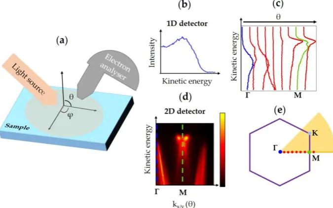
41
In this review the preparation methods employed to produce 2D material are discussed briefly,
42
and include: Chemical Vapor Deposition (CVD) [7], Physical Vapor Deposition (PVD) [8] and
43
mechanical exfoliation. The latter is the easiest way to prepare high-quality 2D materials in a
44
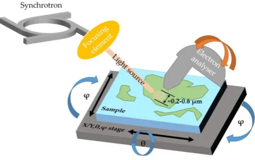
laboratory; it can be applied to the most innovative materials because it is feasible as soon as small
45
bulk pieces of a material are produced. The exfoliated flakes have typically micrometric lateral
46
dimension, but it is difficult to thin down the material to a single layer homogenously. However, the
47
sampling area of a conventional ARPES experiment ranges from tens of micrometers, at synchrotron
48
ARPES facilities, to millimeters in laboratory facilities and therefore it is the principal limitation on
49
the application of ARPES to exfoliated 2D materials.
50
An ideal experiment to study the band structure of 2D materials should allow the visualization
51
of the sample in the macro or nanoscale, utilizing a small portion of sample material to obtain ARPES.
52
In the past few years instrument advances have been made to allow complex measurement
53
operations to be performed at synchrotron light facilities and using laboratory-based equipment. In
54
this review the operating principles of the spatially localized ARPES systems will be presented. First,
55
an overview of early ARPES measurement setups will be discussed before describing state-of-the-art,
56
spatially resolved ARPES equipment.
57
This paper, features some of the most interesting results obtained to date on graphene, TMDCs
58
and 2D heterostructures, along with discussions about future instrument upgrades for spatially-,
59
spin- and time-resolved acquisitions. Graphene represented a starting point for the investigation by
60
spatially localized ARPES of 2D materials, an example of advanced spatially localized investigations
61
on polycrystalline few layer graphene is reported in detail [7]. TMDCs have intriguing electronic,
62
spintronic and photonic properties, the study of their band structure is of fundamental importance;
63
examples of the most well-known TMDC, namely, MoS2 [9], and most innovative such as TiSe2, VSe2
64
[10] and ReS2 [11, 12] are given. In the section on 2D heterostructures several examples of
65
graphene/TMDC composites are presented. Graphene is often used as an active component of the
66
heterostructure [13] but cases where graphene is employed as protective capping layer [14, 15] as
67
well as a conductive substrate [11, 15] have also been reported. A rare example of a study on an
all-68
TMDCs heterostructure is presented [15] exemplifying the strength of this technique for the study
69
innovative ultra-thin 2D devices.
70
2. Spatially localized ARPES setups: technical considerations
71
2.1. ARPES technical considerations
72
The ARPES technique requires an instrument setup that allows: (i) the possibility to investigate
73
the photoemission intensity as function of emission angle and (ii) the ability to distinguish the kinetic
74
energy of the photoelectrons. A sample for ARPES must be crystalline to possess an ordered band
75
structure, and its surface must be smooth to conserve the k-parallel component from the crystal to
76
the vacuum [16]. The surface must be ultra-clean because the sampling depth is typically only few
77
nanometers. ARPES is therefore performed in ultra-high vacuum (UHV) chambers to analyze a clean
78
surface and to ensure that gas molecules do not scatter the low energy photoelectrons.
79
In the very first ARPES experiments, the samples were a few millimeters wide and
80
photoelectrons were detected using a hemispherical analyzer with a small acceptance angle and a
81
simple counter detector. The role of the electron analyzer is very important; indeed, it is the element
82
that allows one to measure the photoelectron kinetic energy, creating, with the simplest 1D detector,
83
an intensity versus kinetic energy spectrum (Figure 1b). In the early experiments, electron analyzers
84
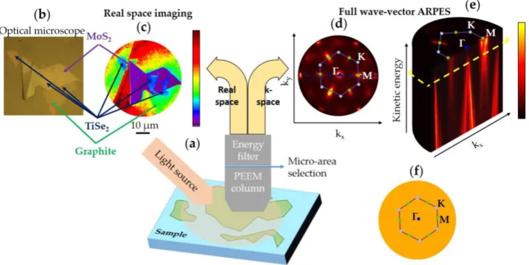
were also used to select a small solid angle of the whole photoelectron emission cloud, which
85
corresponded to a small portion of the k-space [16]. Samples were illuminated with synchrotron light
86
or discharge lamps over a relatively large and homogenous area, see Figure 1a. When the analyzer
87
was positioned at the sample normal, the photoelectrons emerging from it came from the Γ point i.e.
88
the center of the Brillouin zone, see Figure 1b and e. To perform ARPES the sample had to be rotated
89
in both polar and azimuthal angles so that the electron analyzer acquired photoemission spectra at
90
different angles (Figure 1c). By combining the photoemission signal acquired at different angles a
91
reconstruction of the band structure of the material may be obtained.
92
With 1D detector mapping the acquisition of a full band structure was time-consuming and
93
required complex sample movements. The introduction of 2D electron detectors provided the means
94
to reduce the number of sample rotations, as illustrated in Figure 1d. Electron analyzers equipped
95
allowing the acquisition of one slice of the k-space, as shown in Figure 1d and e, which can be
97
equivalent to a polar scan with a 1D detector (Figure 1c). This technological improvement drastically
98
increased the quality of spectra obtained and decreased the acquisition times for conventional
99
ARPES. The significance of this advance can be seen by comparing Figure 1c and 1d.
100
A recent enhancement made to these analyzer systems has enabled angular scans to be made in
101
two dimensions in k-space without tilting or rotating the sample. The scanning of k-space is carried
102
out electronically using dedicated deflectors. An example representation of the region of k-space that
103
can be sampled with these state-of-the-art detectors is represented by the orange shaded area in
104
Figure 1e. Consequently, using such state-of-the-art electron analyzers, a sector of k-space can be
105
acquired; with a suitable photon source energy it is possible to acquire a representative set of high
106
symmetry points without any mechanical movement of the sample. Keeping the sample in the same
107
position during k-space mapping is a crucial requirement for obtaining spatially localized ARPES.
108
109
Figure 1. (a) Conventional ARPES scheme, θ and φ represents the polar and azimuthal angles
110
respectively. (b) 1D detector spectrum in Γ, blue point in (e). Using 1D detectors spectra must be
111
acquired for every θ and φ. (d) Series of 1D acquisitions in a polar scan, the blue and green spectra
112
represent data acquired for the material at Γ and M points respectively. The location of the spectra in
113
the 1st Brillouin zone of the example material (TiSe2) is represented by the dots in (e). (d) Example of
114
a 2D detector acquisition. The blue and green dashed lines mark Γ and M points respectively. The
115
acquisition plane is represented by the yellow line in (e). (e) Representation of the 1st Brillouin zone
116
of the example material, three of the high symmetry points Γ, M and K are marked; the purple solid
117
line represents the 1st Brillouin zone of the material. Shaded orange area sketches the acquisition sector
118
of a 2D analyzer with deflection mode.
119
2.2. Spatially localized ARPES
120
Considering the complex procedure required to perform conventional ARPES from large area
121
samples, it is understandable that to perform ARPES on micro- or nano-sized samples poses a
122
significant technical challenge. Instruments need to scan a vast region of the sample surface in real
123
space (X/Y plane) to find the interesting regions, typically microns wide, and then perform ARPES
124
on them. Nowadays there are different setups available to research and industry to be able to do
125
spatially localized ARPES, and the instrument configurations can be divided into two categories:
126
1. setups that present extremely small light spots, and surface mapping is done by moving the
127
sample with respect to the light;
128
2. setups that allow visualization of the real and k-space extracting electrons with strong electric
129
fields.
130
For the first category, the spatially localized ARPES is typically carried out at synchrotron light
132
sources, see Figure 2. They differ from classical ARPES beamlines in the focusing of the beam by
133
dedicated focusing elements. Synchrotron light is required to have a high brightness and photon flux
134
to offset the strong attenuation by the focusing elements.
135
With these setups it is possible to visualize samples in real space by mounting them on
136
motorized stages (Figure 2) and collecting photoelectrons as function of the sample position. The
137
lateral resolution is directly linked to the beam spot size, the smaller the spot the better the lateral
138
resolution.
139
ARPES mapping is acquired either by moving the electron analyzer in UHV over a range of
140
different emission angles, which is the configuration used at the Spectromicroscopy beamline in the
141
Elettra synchrotron [17], or, most commonly, by rotating the sample with respect to a fixed analyzer,
142
shown by the arrows in Figure 2. The latter configuration introduces the non-trivial issue of keeping
143
the photon beam in the same sample position while rotating the sample but allows the use of a large
144
hemispherical electron analyzer not movable under UHV conditions. This setup is employed at the
145
beamlines I05 in Diamond, ANTARES in Soleil [18] and MAESTRO in ALS. All of these facilities refer
146
to spatially localized ARPES as “nano-ARPES” because the light spot can be focused to
nanometer-147
sized spots [19]. The use of state-of-the-art hemispherical electron analyzers with a deflection mode,
148
as in ANTARES, allows the sample to be kept fixed and the measurement of a larger sector of k-space
149
to be acquired, as seen in Figure 1e.
150
The synchrotron light source is important not only for the brilliance of the light, but also allow
151
to perform ARPES at different photon energies and polarizations. Moreover, the broad range of
152
photon energies available allows X-ray photoemission spectroscopy (XPS) to be performed. The
153
ability to perform spatially localized core-level spectroscopy gives a much deeper insight into surface
154
conditions such as composition, oxidation and contamination.
155
156
157
Figure 2. Schematic representation of spatially localized ARPES with synchrotron light source setup.
158
The radiation from the synchrotron is focused on a spot of few hundreds of nanometers. The sample
159
can be visualized by scanning the real space (X/Y) and collecting photoelectrons with the energy
160
analyzer. To perform the angle resolved acquisition either the analyzer can move as represented by
161
the orange arrows (Spectromicroscopy setup) or the sample can rotate (blue arrows, ANTARES, I05,
162
MAESTRO setups). The electron analyzers are equipped with 2D detectors (see Figure 1d) and
163
therefore they can analyze a portion of the 2D space (see yellow line in Figure 1e) without moving the
164
sample. If equipped with deflectors, as in ANTARES, it becomes possible to visualize a sector of the
165
k-space without moving the sample.
166
For the second category, the photoelectrons are accelerated by means of an extractor towards an
167
electron optical column, which contains electrostatic or magnetic electron lenses, corrector elements
168
such as stigmators and deflectors, apertures in the image plane and contrast apertures; these
169
instruments are usually referred to as Photo Electron Emission Microscopes (PEEMs), see Figure 3a.
170
different angles (k-space) (Figure 3d-e), and by imaging the sample in real space identifying the
172
features of interest (Figure 3b-c); several field of views are available both for real and reciprocal space.
173
Apertures positioned in the image plane are used to select a micro-portion of the sample whereas
174
contrast apertures select specific emission angles.
175
These instruments allow the sample to be imaged without moving it either in real or reciprocal
176
space (Figure 3c-d). This important feature solves major alignment, rotational and movement
177
problems under UHV conditions. Another advantage of these setups is that the zones selected for
178
micro-ARPES and the lateral resolution are not dependent on the light spot size, therefore laboratory
179
light sources such as discharge lamps can be used, making it feasible to have PEEM on UHV
180
laboratory-based platforms.
181
However, a PEEM column cannot filter the photoelectron kinetic energy, therefore it is missing
182
an ARPES measurement requirement. To distinguish the kinetic energy of photoelectrons, PEEMs
183
must be equipped with energy filters that allow one to scan the photoelectron kinetic energy
184
spectrum, these more complex setups are called energy-filtered PEEM (EF-PEEM). The ARPES
185
mapping operation is acquired by imaging at a range of kinetic energies the full-wave vector
186
landscape (Figure 3d), allowing direct imaging of isoenergetic slices of the band structure (see Figure
187
3d and yellow dashed plane in Figure 3e). The full 1st Brillouin zone can be acquired without moving
188
the sample in micron-sized areas, see Figure 3d-e-f. It should be noted that the isoenergetic images,
189
both in the real and reciprocal space, are acquired with no electronic and/or mechanical scanning, but
190
by capturing a single snapshot of the complete field of view presented by the instrument; this ability
191
enables very fast acquisitions.
192
Included among the available commercial EF-PEEM instruments are the ScientaOmicron
193
NanoESCA II, the Time-of-flight (TOF) PEEM of Focus, the METIS and FE-LEEM (low energy
194
electron microscopy)/PEEM P90 of SPECS and the ELMITEC PEEM/LEEM. The energy selection in
195
these instruments is done in a range of different ways, including using hemispherical analyzer(s),
196
TOF filters and electrostatic/magnetic retarding optics.
197
The best energy resolutions are obtained by the hemispherical analyzers and TOF, for example
198
NanoESCA II is equipped with two hemispherical analyzers coupled in a “S” fashion to minimize
199
the aberrations [20], and with these setups the achievable energy resolution is typically of the order
200
of few tens of meV. The PEEM/LEEM instruments do not excel in energy resolution, however, they
201
are very versatile instruments and with their electron source they can perform low energy electron
202
diffraction (LEED) in micro-spot mode and visualize single atomic steps [21].
203
All these instruments have a lateral resolution in the nanometer range, LEEMs in this respect
204
typically out-perform PEEMs, but in any case, spatially localized ARPES is usually performed over
205
an area of a few microns and limited by the fact that the area is selected by means of a mechanical
206
aperture.
207
Laboratory based equipment use typically discharge lamps, such as He discharge lamp that
208
offers 21.2 eV (He I) or 40.8 eV (He II). The poor photon tunability does not represent a problem for
209
single layer 2D materials because they do not have a kz dispersion, but it is a limitation for 3D
210
materials where synchrotron tunable radiation must be employed to perform kz dispersion. Indeed,
211
several EF-PEEM are installed on synchrotron light source facilities to offer the combination of high
212
flux and versatility of synchrotron light with the fast imaging and stability of the PEEM. Almost all
213
the synchrotron light facilities host a PEEM beamline, among those facilities there are NanoESCA
214
[22] and Nano-spectroscopy beamlines in operation at ELETTRA, I06 at Diamond, HERMES at Soleil,
215
217
Figure 3. (a) Schematic representation of spatially localized ARPES acquired by a EF-PEEM. (b-c) Real
218
space sample visualization of a 2D heterostructure. (b) Optical microscope image. (c) Real space image
219
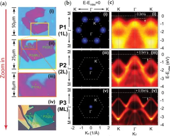
obtained with a single snapshot of 20 seconds acquired close to the work function threshold. The areas
220
of interest can be selected by micro-apertures in the image plane. (b-c) Blue, purple and green arrows
221
represent TiSe2, MoS2 and graphite flakes respectively (d) Single snapshot of full wave vector slice of
222
60 seconds of TiSe2 acquired from one single flake of about 20 microns. The kinetic energy of the image
223
(d) corresponds to the dashed yellow plane in (e). (e) Series of snapshots at different kinetic energies
224
to form a complete ARPES map, the data cube has been cut along the dashed blue line in (d). The cut
225
data shows the classical ARPES acquisition, i.e. kinetic energy vs electron momentum. (f)
226
Representation of the 1st Brillouin zone of the example material, in orange circular the field of view of
227
the full-wave vector ARPES in (d) and (e). (d-e-f) Three of the high symmetry points are marked with
228
Γ, M and K; the blue dot, the green dots and light blue represent the Γ, M and K point respectively.
229
The purple solid line represents the 1st Brillouin zone. The real and reciprocal space images reported
230
in this figure were acquired at Bristol NanoESCA facility and have not been published previously.
231
It is important to note that using a technique called dark-field PEEM a portion in k-space and
232
energy can be selected [23]; this defined element in k-space, e.g. a Dirac cone, can be used as source
233
of signal to image the sample in real space, allowing the identification of the material portion where
234
the k-space feature arises. These acquisitions can be performed with EF-PEEMs [23] and in some
235
nano/micro-ARPES beamlines such as Spectromicroscopy [24] and ANTARES [18].
236
3. Spatially resolved ARPES for 2D materials
237
Spatially localized ARPES has been developed for being able to analyze micro- or nanometric
238
samples, consequently it is strongly linked to the lateral dimensions of the materials. Several
239
technological challenges arise from the production large flakes of 2D materials, therefore it is
240
important to understand how they can be synthesized. Three different techniques to grow 2D
241
materials have been reported:
242
243
1. Epitaxial growth by CVD or PVD. This method allows flat and azimuthally oriented
244
layers to be deposited on large single crystal substrates. It is easy to control the number
245
of layers by changing the deposition time, growth chambers can be directly mounted
246
onto ARPES equipment and samples can be transferred under UHV conditions. With
247
epitaxial films it is not necessary to employ spatially resolved ARPES to limit the
248
analyses region on single material grains because the grains are azimuthally oriented
249
with the substrate and form a macroscopic continuous ordered crystalline lattice.
250
Because the large amount of signal available for ARPES, advanced analyses such as
spin-251
disadvantages of this method: it is time consuming, because evaporators and setups
253
must be carefully optimized for every different material; secondly, the interaction
254
between the substrate and 2D materials is so strong that usually it is not feasible to
255
transfer the 2D layers onto other substrates.
256
2. Conventional CVD produces large micron-scale grains azimuthally misaligned. In
257
respect to the epitaxial growth, the control of the number of layers it is more difficult
258
and occasionally multi-layers are produced. Furthermore, this method is more prone to
259
contamination because it is usually performed under non-UHV conditions. The
260
advantage of conventional CVD with respect to epitaxial growth is that it is possible to
261
use single crystal and polycrystalline substrates with weaker bonds to the 2D material,
262
allowing their detachment and transfer.
263
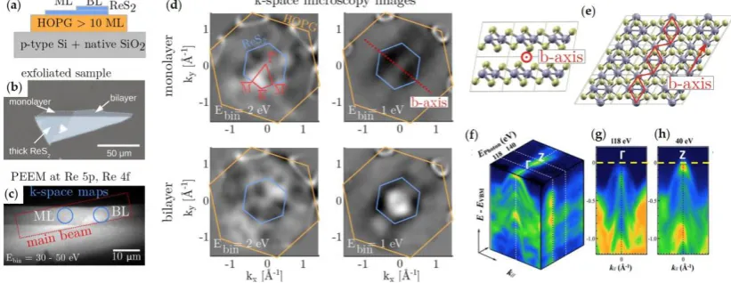
3. Mechanical exfoliation, also called “adhesive tape technique”, produces extremely
264
high-quality layers because the starting point are ultra-pure single crystals. The main
265
drawbacks are the micron-size of the layers and that the thickness is not easily
266
controllable. This technique is the main method used for studying promising new 2D
267
materials because it is fast and easily achievable, exploiting the ease of exfoliation along
268
the weak van der Waals inter-layer bonds. Importantly, it is the main technique to form
269
2D heterostructures.
270
271
Not all the materials can be prepared by all these methods. Some analogues of graphene such as
272
silicene [25] and germanene [26], and some TMDCs such as PtSe2 [27] are obtainable with good
273
quality only by epitaxial methods. Indeed, spatially localized ARPES is ideally suited to the analysis
274
of samples prepared by CVD and mechanical exfoliation and their heterostructures. Arguably the
275
most interesting samples for study are the mechanically exfoliated ones, due to their formation in
276
micrometric flakes with multiple layers. These can be used to analyze the changes in band structure
277
and electronic properties with different numbers of layers on a single sample. For the most
278
challenging 2D material analyses, spatially localized ARPES is also used to analyze bulk crystals,
279
which, at the beginning of the material growth optimization, present only a few microns of clean
280
terraces. The typical procedure followed for the analysis of a new 2D materials would be:
281
1. Characterize the bulk material band structure;
282
2. Study 2D exfoliated layers to observe quantum confinements effects and any difference
283
with respect to the bulk;
284
3. Identify a method to produce large 2D layers and perform advanced characterizations
285
such as spin-resolved, or time-resolved ARPES studies.
286
287
Some examples of spatially localized ARPES studies on graphene, TMDCs and 2D
288
heterostructures, are presented below which show how insightful this technique can be for exploring
289
the 2D materials world.
290
3.1. Graphene and its analogues
291
The starting point of ARPES investigations on 2D materials has been graphene, and the
292
development of spatially localized ARPES setups has to some extent been driven by graphene [2, 28]
293
and more recently by other 2D materials [3]. Nowadays graphene and graphite are so well known
294
that they are used as calibration samples in ARPES facilities [18].
295
Graphene is a single layer of sp2 hybridized carbon atoms. In this material electrons and holes
296
act like Dirac fermions with zero mass and zero bandgap, therefore it is considered a semimetal.
297
Charge carriers are mass-less, relativistic Dirac fermions with the points of intersection between the
298
conduction and valence bands being called Dirac points. The energy versus k dispersion curves of
299
electron and holes form two-dimensional cones around the Dirac points (see Figure 4b), which are
300
usually referred to as “Dirac cones”; for a charge neutral layer the “Dirac point” is at the Fermi level.
301
ARPES can image directly the Dirac cones and electronic information can be extracted such as
303
doping [29], i.e. the difference between Fermi energy and Dirac energy, Fermi velocity [30] and many
304
body interaction, such as electron-plasmon and electron-phonon coupling [31].
305
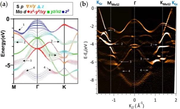
The atomically thin nature of graphene makes its electronic properties strongly influenced by
306
the substrate and any surrounding ultra-thin layers. Graphene has been extensively studied by
307
conventional ARPES because it is relatively easy to obtain epitaxial layers by dosing carbon
308
precursors on a hot catalyst single crystal substrates, such as Ni(111) [32, 33]and Ru(0001) [34]. Its
309
band structure has been comprehensively investigated as a function of the metal substrate by ARPES;
310
it has been found that some metals interact so strongly with graphene that they cause a drastic change
311
in its band structure [32, 35-37], while others are considered weakly interacting and graphene placed
312
on them is considered quasi-freestanding [32, 33, 38]. To modify graphene/substrate interaction a
313
methodology, called intercalation, has been developed to allow the exchange of graphene support.
314
In these types of experiments, graphene is exposed to an agent that can intercalate it, i.e. it positions
315
itself in between graphene and substrate. Another interesting method to modify graphene is the
316
doping by alkaline metals deposited on top of it [39, 40]. This doping method is also used for 2D
317
semiconducting layers to visualize their conduction bands as reported later in this review.
318
The properties of graphene in contact with different species such as substrates, intercalating
319
agents and deposited species, can be studied by ARPES. For example graphene intercalated with
320
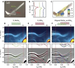
weakly interactive metals or oxygen can remove hybridization with the substrate [32, 36, 38, 41],or
321
strongly interactive metals can deliberately induce hybridization to tune the material properties [42,
322
43]. For example, graphene spin degeneracy can be lifted by intercalation of 1 mono-layer (ML) of
323
ferromagnetic metals [42], or a particular spin structure can be obtained intercalating 1 ML of low
324
interactive metal underneath graphene grown on a ferromagnetic substrate [36]. Spin sensitive
325
detectors for ARPES are essential to understand the graphene spin structure [36] and, as reported
326
later, they are even more important for some semiconducting TMDCs for their intrinsic spin-splitting
327
band structures.
328
The studies on spatially localized ARPES on graphene have been fundamental for the
329
investigation of azimuthally disordered CVD-grown graphene. This analysis has been carried out
330
with graphene on copper [7, 44-52], on platinum, [42, 53, 54], on silicon carbide [55, 56], or to study
331
multi-layer regions that do not cover all the surface, such the one found on copper [7] and ruthenium
332
[57, 58].
333
One important study that emphasizes the power of spatially localized ARPES for graphene was
334
carried out with multi-layer graphene on copper [7]; part of the main results of this work are reported
335
in Figure 4. In this study [7] micro-ARPES has been carried out on graphene and twisted multi-layers
336
of graphene. The aim of the paper was to study the evolution of the doping caused by the substrate
337
(Figure 4a-c) and to study the interaction between the layers (Figure 4d and e). In respect of doping,
338
it has been found that with increasing numbers of layers, the top layer of graphene becomes less
339
electron-doped, i.e. the Fermi energy it is closer to the Dirac energy (see Figure 4b), which can be
340
explained by an effective capacitor model of the multilayer system. Due to the existence of an effective
341
work function difference, the electrons will transfer from the copper substrate to the graphene, filling
342
the unoccupied states, which causes the doping effect (see Figure 4b). As the number of layers
343
increases, the top layers are shielded from the substrate, and accumulate fewer transferred electrons
344
than the lower layers, see Figure 4b and 4c. The interest in studying the interaction between the layers,
345
is related to the way in which the twisted multilayers interact each other and form van Hove
346
Singularities (vHS) that are detectable by mapping the band structure of bi-layers and multi-layers
347
twisted at angles of up to 31°. Figure 4d and 4e show the vHS analysis for a bi-layer twisted by 8.2°,
348
the band structure of the two layers clearly interacts, and there is a decrease of the photoemission
349
intensity where the two Dirac cones intersect, as seen in Figure 4e. In both aspects performing ARPES
350
in a micro-portion (see Figure 4a) of the sample has been essential to visualizing the doping trends
351
353
Figure 4. (a) Large-scale spatially scanned image of the graphene and few layer graphene on copper
354
foil obtained by acquiring photoelectrons in the spectral range of the copper d-bands. Dots with
355
different color mark selected positions for subsequent measurement. (b) Energy–momentum–
356
dispersion taken at positions shown in (a). Red dashed lines indicate the energy of the Dirac point
357
(ED) in each spectrum of the top layer. Red solid curves are integrated energy distribution curves
358
(EDCs) for each spectrum, which are corrected by the Fermi–Dirac distribution, allowing one to see
359
features near the Fermi surface. (c) Evolution of the value of ED measured from the top layer with total
360
number of layers. The blue line indicates a fit of the data using the capacitor-model. (d) (i) Equal
361
energy contours of twisted bi-layer graphene band structure with twist angle 8.2° showing two Dirac
362
cones. (ii) Comparison between measured and illustrating energy contours. The dotted red curves are
363
calculated from a tight binding model for the overlapping bands from two Dirac cones without
364
hybridization. The solid blue curves show a guide to the eye to illustrate the hybridization effect. The
365
mini gaps marked by green arrows stem from a Moiré super-potential. (e) Energy–momentum–
366
dispersion passing through the two Dirac points and the vHS. The right panel shows the integrated
367
EDC over the region shown above. Adapted from Ref. [7] with permission of © 2017 WILEY-VCH
368
Verlag GmbH & Co. KGaA, Weinheim
369
The example study reported in Figure 4 [7] also demonstrated that it is very important to map a
370
relatively big portion of the k-space (see Figure 3d,e,f) to perform cuts, i.e. energy versus k//, in all the
371
desired directions. For example, the spectra in Figure 4b are acquired in the perpendicular direction
372
of the ΓK direction whereas in Figure 4e the cut is along the two Dirac points of the twisted layers.
373
The ability to map a sector of the k-space also allows one to obtain isoenergetic maps as shown in
374
Figure 4d and Figure 3b. In this respect instruments that can perform full wave vector ARPES, such
375
as the EF-PEEM, will probably be favoured for such complex acquisitions in the future.
376
Important spatially localized ARPES studies have been acquired on mechanically exfoliated
377
graphene flakes [59], on bi-layer graphene to study the vHS [45, 60] and 2D heterostructures, the
378
latter are reported later in this review. Because spatially localized ARPES setups can also visualize
379
the material in the real space (see discussion in section 2.2 and Figure 4a) studies of reaction processes
380
involving graphene, such as oxidation or intercalation, can be carried out in real time, especially using
381
PEEM (see discussion in section 2.2). ARPES analysis can link the material transformation and
382
chemical reaction with changes in electronic properties. [44, 61, 62].
383
384
All these studies focused on graphene demonstrate a methodology that can be applied to the
385
study of other 2D materials, confirming the pivotal role that graphene had as the prototype 2D
386
Hexagonal boron nitride (h-BN), the analogue of graphene with boron and nitrogen atoms, has
388
been synthesized and studied in a similar fashion to graphene. It is an insulator with a band gap of
389
more than 5 eV [63] and therefore represents a fundamental component of future 2D electronic
390
devices. Hexagonal boron nitride single layer has been grown on epitaxial substrates and intercalated
391
to obtain a quasi-free-standing layer and this change has been visualized by conventional ARPES [64,
392
65]. It has also been mechanically exfoliated and analyzed by nano-ARPES [66], exactly as has been
393
done previously with graphene.
394
Another interesting analogue of graphene is phosphorene, i.e. a single layer of black
395
phosphorous. It has a notable technological advantage when compared with graphene which is a
396
direct and sizeable band gap for a mono-layer up to bulk films in the eV range, making it very
397
interesting for optoelectronic devices [67]. Phosphorene is obtainable by mechanical exfoliation of
398
black phosphorus but interestingly only the bulk material has been extensively studied by ARPES
399
[68-74]whereas the mono-layer has not been investigated yet, probably because it is prone to air
400
oxidation [75]. As reported later in the heterostructure section 3.3, advanced techniques for the
401
protection by encapsulation with oxidation resistant materials, such as graphene and h-BN [14], will
402
be probably applied to obtain single layer phosphorene band structure by spatially localized ARPES.
403
3.2. Transition metal dichalcogenides
404
TMDCs are a very important class of 2D materials. They comprise three atom layers, a central
405
layer composed of a transition metal and an upper and lower layer made up of chalcogenide atoms,
406
typically sulfur, selenium and tellurium [76]. In contrast to graphene an individual TMDC
mono-407
layer can have different phases, the most typical for mono-layer are the so-called 2H and 1T, which
408
have a AbA and AbC staking, respectively (with the capital and lower case letters denote chalcogen
409
and metal atoms, respectively) [76].
410
So far, group VIB TMDCs have kindled the greatest amount of interest among researchers in the
411
electronic, optoelectronic and spintronic fields [77]. Several TMDCs of this group are semiconductors
412
with a band gap in the eV range, therefore they can be efficiently integrated into ultra-thin field-effect
413
transistors (FET) devices. This has been the prime motivation for researching them. Their intrinsic
414
semiconductor characteristic is responsible for promoting a good on/off ratio in FET devices easily
415
outperforming graphene with its semi-metallic band structure. Molybdenum and tungsten
416
chalcogenides are naturally layered materials with a 2H stacking. Their band structure varies as
417
function of the number of layers; in their bulk form, most of these TMDCs present an indirect-gap
418
characterized by a valence band maximum (VBM) at the Γ point and a conduction band minimum
419
(CBM) at the midpoint Σ along the Γ–Κ high symmetry directions. When the thickness is reduced to
420
a single mono-layer, the band gap becomes direct at the Κ-points.
421
The modification of the band structure as function of the number of layers for MoS2 has been
422
demonstrated by micro-ARPES [9, 78], this transformation arises from quantum confinement effects.
423
In Figure 5 an example of micro-ARPES on MoS2 exfoliated flakes is reported. In Figure 5a optical
424
and PEEM images of the sample are presented, while in Figure 5b and 5c VBM and ARPES along Γ
-425
K direction are shown, respectively. The switch of VBM from mono-layer to thicker layers is clearly
426
detectable comparing the results in Figure 5b. With this experiment of spatially resolved ARPES on
427
only one deposited sample has been able to prove the modification of the band structure of ultra-thin
428
TMDCs layers, proving once again the strength of this technique combined with mechanical transfer
429
431
Figure 5. Band valley evolution from multi-, bi- to mono-layer MoS2 nanoflakes. (a) 2D photoemission
432
spectra intensity contrast map of MoS2 flakes (measured at the Fermi level), with different
433
magnifications from large area (i) to small area (iii), showing the procedure to locate the targeted
434
mono-layer flake. Panel (iv) gives the optical image of the same flake, where the mono-, bi- and
multi-435
layer MoS2 flakes can be clearly seen. Points P1−P3 indicate the three measurement positions for
436
mono-, bi-, and multi-layer MoS2 flakes. (b) Constant energy plots measured at mono-layer (point P1),
437
bi-layer (point P2), and multi-layer (point P3) regions, with the energy positions at E − EVBM = 0 eV. (c)
438
Band dispersions along the high symmetry K−Γ−K direction from points P1−P3, showing the band
439
valley evolution with different flake thicknesses. Adapted with permission from Ref. [9]. Copyright
440
2016 American Chemical Society.
441
One fascinating feature of this class of semiconducting TMDCs is their band structure around
442
the K points which is composed by two spin-polarized branches [79]. For example, mono-layer WSe2
443
VBM is characterized by two bands with a spin-splitting of about 0.5 eV, making this material one of
444
the most studied for spintronic devices [80, 81]. For this class of materials, the implementation of a
445
spin-resolved detector for ARPES is of crucial importance. Until now the spin-resolved ARPES
446
studies have been conducted on bulk TMDCs [82-85] and on epitaxially deposited TMDCs [80]. These
447
studies are rare and challenging because they need high brightness and long acquisition times;
448
consequently, the reduced light intensity experienced with micro/nano ARPES makes these
449
acquisitions very challenging. However, a recent development in PEEM at the NanoESCA beamline
450
in Elettra which has been equipped with a spin-detector [86] will probably solve this problem
451
allowing the full wave-vector spin-resolved ARPES measurements to be made on small exfoliated
452
flakes [87].
453
Because several TMDCs are semiconductors it is of pivotal interested to study their conduction
454
band, and this is accomplished by two approaches: (i) deposition of alkaline metals followed by
455
ARPES, (ii) time resolved pump and probe ARPES.
456
As stated above for graphene, doping the surface by deposition of alkaline metals it is a
well-457
known method to shift the Fermi energy of the material and, in the case of semiconductive TMDCs,
458
to access the CBM [8, 9, 88-90]. The alkali metal deposition can also cause modification of the band
459
structure of the material because it creates an electric field perpendicular to the sample surface; it has
460
been found that this field can induce a Stark effect [89, 91, 92] and change from an indirect to direct
461
band gap bulk MoSe2 [89].Another interesting feature is the formation of a two-Dimensional Electron
462
Gas (2DEG) on the sample surface after the alkali metal deposition, opening new opportunities for
463
ARPES where the sample has been doped with alkaline metals [93] are rarely presented probably
465
because of the intrinsic complexity of depositing metal during the ARPES acquisitions. For instance,
466
in EF-PEEM instruments there is only a limited space, typically a few millimeters, between sample
467
and the extractor lens.
468
Another way to study the conduction band of the sample is time-resolved ARPES to perform
469
pump and probe experiments. In these experiments two photons with a femtosecond delay are sent
470
to the sample; a photon called “pump” has the function to excite electrons into the conduction band,
471
while the other called “probe” has the role of extracting photoelectrons. This technique is used to
472
reveal the dynamics of the charge carriers and it is the only method able to visualize the electron
473
relaxation path in excited states with momentum resolution [94]. Similar to spin-resolved ARPES,
474
time-resolved ARPES has been carried out on bulk crystals [94]or epitaxially-grown MoS2 [95, 96],
475
because their large area overcomes the usual problems of low signal and the long acquisition times.
476
Future enhancements to this type of technique include the employment of time-resolved sources for
477
EF-PEEM [97] and TOF PEEM [98, 99]; it is envisage that the latter will be crucial in the future to
478
perform spatially- and time-resolved ARPES.
479
Other TMDCs, such as TiSe2 and VSe2 are metallic, they have a 1T stacking and they show low
480
temperature transitions to states with charge density waves (CDW) leading to periodic modulations
481
of the electronic charge density. The resulting superlattices can be either commensurate or
482
incommensurate and the CDW ordering can compete with other phenomena such as
483
superconductivity and anti-ferromagnetism. ARPES investigation of these materials is still in the
484
early stages, they have been only analyzed by ARPES in their bulk form [100, 101], or as epitaxial
485
mono-layers [100, 102].
486
Figure 6 shows micro-ARPES acquisitions on TiSe2 and VSe2 small bulk crystals. The CDW
487
effects in TiSe2 are visible in the acquisitions along the ΓM direction; the replica of the
488
photoemission features in Γ, due to the Se 4p orbitals, is visible in Figure 6b at the M point (red circle).
489
The replica is due to the formation of the (2×2) CDW phase [100]. The band structure modifications
490
due to the CDWs in VSe2 are much more subtle and they are still under investigation [10]. Their
491
visualization requires snapshots of the Fermi surface as illustrated in Figure 6c and 6d, which show
492
well defined “pockets” surrounding the M points. Acquiring Fermi surface snapshots at different
493
temperatures in the CDW phase, a small gap opening (few meV) is observable which induces a
494
reduction in intensity along the K’-M-K direction, shown as red circles in Figure 6c and 6d, whereas
495
other parts of the “pockets” do not decrease in intensity at the same rate (blue circles). It is important
496
to note that these latter measurements are extremely complicated to acquire with conventional 2D
497
detectors because several azimuthal rotations are needed to investigate a whole “pocket”, the use of
498
full wave-vector ARPES notably improved the acquisition times for such complicate experiments.
499
500
Figure 6. Example of TMDCs with CDWs. (a,b) TiSe2 bulk ARPES acquisition along ΓM direction
501
at (a) 300 K and (b) 31 K. The CDW folding of the band structure is detectable for the replica at low
502
temperature for the Se 4pfeatures at the Γ point, red circles zones. The Γ and M points are indicated
503
by dashed white lines. (c,d) VeS2 bulk ARPES Fermi surface snapshot at (c) 120 K and (d) 40 K. The
504
CDWs Fermi surface gapped and un-gapped regions are indicated by the red and blue circles,
505
respectively. The purple solid line represents the 1st Brillouin zone of the material, the white dots and
506
letters indicate the high symmetry points. All these images were acquired at the Bristol NanoESCA
507
A recently studied TMDC is ReS2 for its unusual in-plane anisotropy. The ReS2 structure is
509
considered a distorted 1T crystal structure and compared to the 2H structure of group VIB TMDCs
510
an additional valence electron leads to the formation of Re chains along the b-axis of the crystal, see
511
scheme in Figure 7e. The low crystal symmetry results in highly anisotropic optical, vibrational, and
512
electron transport properties and therefore adds an additional degree of freedom for applications in
513
sensor and electronic devices. This material is at a very early stage of its study, therefore studies of
514
spatially localized ARPES are pivotal not only for probing layers with different thickness [11] but also
515
for investigating small bulk pieces [12, 103]. Figure 7a-b features the first spatially localized ARPES
516
on ReS2 single and bi-layers. While Figure 7f-g shows the ARPES from a small bulk crystal using
517
different photon energies to explore the kz dispersion. From the full wave-vector ARPES reported in
518
Figure 7b the predicted lack of hexagonal symmetry of this material is easily detectable. The unusual
519
symmetry has been proven by acquiring a single snapshot exemplifying once again the importance
520
of the full wave-vector ARPES. Interestingly, direct/indirect band gap transition of the ReS2 has not
521
been clearly established and further studies will have to be carried out to fully understand this
522
material.
523
524
525
Figure 7. ReS2 spatially resolved ARPES acquisitions. (a) Sketch of the exfoliated few-layer ReS2
526
sample. (b) Optical microscope image of the sample before transfer onto HOPG. (c) Real space PEEM
527
image with Ebinding integrated over 30–50 eV (Re 5p/Re 4f core levels). (d) Second derivative k-space
528
images selectively measured on the mono-layer and bi-layer areas of the sample with the surface BZ
529
of ReS2 indicated in blue and of HOPG in orange. The high symmetry directions are marked by red
530
lines. (e) Distorted 1T crystal structure of ReS2 with the Re chains forming along the b-axis of the
531
crystal indicated in red. Adapted with permission from Ref. [11]. Copyright 2017 American Chemical
532
Society. Nano-ARPES acquisition of bulk ReS2 (f) nano-ARPES signal (blue = low to orange = high) as
533
a function of energy below the Fermi energy (vertical axis) and in-plane momentum k//, for excitation
534
energies of 118 and 140 eV (left and right respectively). (g) and (h) panels show the nano-ARPES
535
electronic dispersion of the valence bands at the Γ and Z points of the 3D Brillouin unit cell. Adapted
536
with permission from Ref. [12]. Copyright 2017 Springer Nature.
537
The current state of knowledge from ARPES of materials such as TiSe2 [100], VSe2 [10, 101], ReS2
538
[11, 12, 103] and ZrSe2 [90] may be regarded as similar to the early studies of group VIB TMDCs. For
539
example, the first ARPES on single layers WSe2 and MoS2 were performed by micro acquisition on
540
exfoliated flakes [78, 104, 105]. Nowadays, after several studies and through growth optimization,
541
WSe2 and MoS2 can now be grown epitaxially and advanced ARPES methods such as surface doping
542
[9, 90], spin-resolved ARPES [80] and time-resolved ARPES [95, 96] can be carried out. These
543
examples confirm that the union of mechanical transfer and spatially localized ARPES is crucial to
544
the rapidly evolving 2D material world.
545
As reported above, by mechanical transfer it is possible to place samples on an arbitrary
546
substrate and understand how their properties are modified by contact with other species. An
547
of SiOx which confirms the extreme sensitivity of 2D layers to the underlying substrate [106].
549
Examples of spatially-localized ARPES on CVD grown TMDCs is reported for WS2, WSe2 and MoS2,
550
the band structure has been studied by micro-ARPES [78, 81, 107-110]. An interesting study of
551
artificially build bi-layers of CVD-grown MoS2 has been carried out by micro-ARPES; the band
552
structure changes as a function of the angle between the layers and a remarkable dependence of the
553
angle with the electron effective mass and of the position of the bands has been found [109].
554
3.3. Two dimensional heterostructures
555
2D heterostructures are a vibrant research field with the principal aim of creating novel
ultra-556
thin devices with unprecedented properties achieved by combining different 2D materials [3]. So far
557
in this review materials with different electronic structure have been discussed such as semi-metallic
558
graphene, insulating h-BN and semiconducting TMDCs as well as phosphorene; these could be the
559
components of future ultrathin devices utilizing exclusively 2D materials [14].
560
As reported above for the isolated 2D materials, some 2D heterostructures have also been
561
synthesized by epitaxial methods, the advantage of this growth method is the possibility to perform
562
complex ARPES analysis, but they are even more complex to synthesize than the isolated 2D
563
materials. Several epitaxial routes are based on the use of graphene because it is so well-studied that
564
advanced growth on top of it are possible, for example, TMDCs are deposited onto graphene by CVD
565
or PVD. Epitaxial graphene on SiC represents an excellent example of graphene used as a basis for
566
the growth of other 2D materials [81, 96, 111]. Epitaxial heterostructures that do not contain graphene
567
are much rarer in the literature because the materials growth has not yet fully undisclosed and the
568
deposition of different elements can cause undesired mixing and phase changes [64, 112-114].
569
One way to overcome the disadvantage of complex CVD and PVD deposition methods to form
570
heterostructures is the mechanical transfer methods, as mentioned above, which lends itself to
571
spatially localized ARPES. For transferred layers one of the most studied components for
572
heterostructures is graphene or graphite, indeed nowadays, graphenic flakes are used also as a
573
conductive substrate [11, 15] and as an ultrathin capping layer to preserve sensitive materials from
574
oxidation [15].
575
The 2D heterostructures formed by mechanical exfoliation have been extensively used for the
576
study of the electrical, magnetic and carrier transport properties of 2D materials [14, 115-118].
577
Heterostructures composed of graphene and h-BN were the first to be studied, because it was clear
578
that the properties of graphene were strongly influenced by the substrate; hexagonal boron nitride
579
being a flat, insulating and with a dangling bond-free platform was perfect candidate to study
580
graphene pristine properties. [115] Spatially-localized ARPES on graphene/h-BN verified the absence
581
of graphene doping and also measured the replica of Dirac cones due to the Moiré superlattice on the
582
graphene K points [119].
583
Graphene has been coupled with several TMDCs, a lot of studies have been focused on MoS2
584
[13, 120-122] because it was one of the first materials in its class to be extensively studied, its
585
fabrication is well known and it is commercially available as large single crystals.
586
The studies of heterostructures composed of graphene and MoS2 have been focused on studies
587
of band offsets [120, 121], mini-gap interactions [13, 121] and alteration versus layer orientation [13,
588
121, 122]. A strong interaction between graphene and TMDC is visible in ARPES on the bands with
589
an out-of-plane character. In Figure 8 the example of a polycrystalline azimuthally mis-oriented
590
graphene transferred onto bulk MoS2 is reported. In this experiment the azimuthal disorder of
591
transferred graphene made it possible to have on a single substrate several different alignments
592
between the MoS2 and graphene. By using spatially-localized ARPES enabled the study of individual
593
flakes and therefore made it possible to establish the band structure of the heterostructure as function
594
of the layer orientation [13]. In Figure 8a the calculated band structure of MoS2 with the character of
595
the bands for the Mo 5d and S 3p orbitals is presented. Figure 8b shows the nano-ARPES acquired
596
from two flakes of graphene: for negative wavenumber graphene with ΓK direction aligned with
597
the ΓM direction of MoS2, and for positive wavenumber graphene with ΓK direction aligned with
598
crosses a MoS2 feature with an out-of-plane character. For example the gap “1” is due to Mo 5dz2
600
bands and it is visible only when the 2D materials are not aligned, while the gap “2” is visible in any
601
of the two flakes reported in Figure 8b and it is due to S 3pz orbitals [13]. Interestingly this
602
phenomenon has not always been detected; for WSe2/graphite [15], MoSe2 and MoS2/graphene [13,
603
111, 121] it has been observed, however recently for WSe2/graphene it has been not [81], so a more
604
accurate investigation will be necessary to rule the effect of the heterostructures parameters, such as
605
layer separation.
606
607
Figure 8. Example of ARPES from graphene and TMDC heterostructure with gap opening. (a)
608
Calculated band structure of MoS2 with the orbital character of the individual bands color-coded.
609
Adapted with permission from Ref. [123] Copyright 2012 American Physical Society (b) 2nd derivative
610
of E‐k ARPES spectrum of graphene/MoS2 bulk . The observed band gaps in the graphene π‐band are
611
labeled and their respective position with respect to the MoS2 band structure are indicated in (a).
612
Reprinted with permission from Ref. [13] Copyright 2015 American Chemical Society.
613
Few examples exist in the literature that report spatially-localized ARPES on heterostructures
614
that do not contain graphene, one recent example is the heterostructure WS2/h-BN [93]. This
615
composite has been created by mechanical transfer and investigated by micro-ARPES. These
616
measurements provide direct evidence of a trion quasiparticle and give access to both their energy
617
and momentum dependence that is lacking from optical, tunneling or momentum-integrating
618
transport measurements [93].
619
The only example in the spatially-localized ARPES literature reported so far of all-TMDC
620
heterostructures created by mechanical exfoliation has been reported in Ref. [15]; the main results are
621
reproduced in Figure 9. In this work the heterostructure is formed from MoSe2/WSe2, both single
622
layers, and has been studied by micro-ARPES. An optical microscope image of the sample is shown
623
in Figure 9a; ARPES on the single 2D materials and on the heterostructure region is reported in Figure
624
9d-f. The single layer nature of the TMDC is confirmed by the VBM position at the K point for the
625
isolated material. Spatially-localized ARPES acquisition on the heterostructure zone showed that in
626
the proximity of the K point, the bands do not change position, while a new feature is formed at Γ,
627
similar to what has been observed for WSe2 bi-layer. The observations showing that the valence band
628
edge remains at the K point and that the band alignment is type II are both extremely important for
629
electronic and optoelectronic applications. [15]
630
632
Figure 9. Example of all-TMDC heterostructure study by means of ARPES, PEEM and optical
633
spectroscopy. (a) Optical image showing mono-layer MoSe2 and WSe2 sheets, which overlap, with the
634
MoSe2 on top, in an aligned hetero-bi-layer region (H). Their boundaries are indicated with
color-635
coded dotted lines. (b) Angle-integrated spectra in each of the three regions. (c) Map of the energy of
636
maximum emission. (d-e-f) Momentum slices along Γ − K in the three regions, (top) unprocessed and
637
(bottom) twice-differentiated, with cartoons of the structures above. The superposed dashed colored
638
lines are DFT calculations for the MoSe2 mono-layer (green), the WSe2 mono-layer (red), and the
639
commensurate hetero-bi-layer (blue). The white dashes in the lower panel of (f) indicate the VBM in
640
the MoSe2 and WSe2 mono-layers and hence the valence band offset. The white dashed lines in the
641
upper panels of (d) to (f) mark the VBM in the isolated MoSe2 (M) and WSe2 (W) mono-layers and in
642
the aligned hetero-bi-layer (H). Adapted from [15]. Reprinted with permission from AAAS.
643
Complex heterostructures will be available for spatially-localized ARPES studies because of the
644
advance in the mechanical transfer technology to form complex 2D devices for optical, carrier
645
transport, magnetic and spin property characterization [3, 14, 124-127]. It is expected that band
646
structure measurements will integrate information derived from other microscopic techniques and
647
vice-versa. For example, optical spectroscopies can provide information on the number of layers,
648
band positions, exciton formation and the type of band alignment [15, 64, 128-133], but only ARPES
649
allows the direct visualization of the band structure and can elucidate the carrier dynamics [15, 93,
650
94].
651
652
4. Conclusions
653
In this review the principles of spatially-localized ARPES have been reported. Experimental
654
measurement configurations, from early ARPES systems to the most advance state-of-the-art
655
instruments for micro and nano-ARPES have been presented. The technical challenges of using these
656
tools have been discussed and both synchrotron and laboratory-based instruments have been
657
introduced.
658
ARPES using laboratory-based equipment is feasible with crystal domains a few microns across,
659
the light intensity available is typically lower than those at synchrotron facilities, but long acquisitions
660
are possible because longer measurement times can be accessible. Also, they are very stable

![Figure 6 shows micro-ARPES acquisitions on TiSe2effects in TiSephotoemission features in Γ, due to the Se 4The replica is due to the formation of the (2×2) CDW phase [100]](https://thumb-us.123doks.com/thumbv2/123dok_us/8047088.1340390/12.595.93.507.558.673/figure-arpes-acquisitions-effects-tisephotoemission-features-replica-formation.webp)