A Digital Up-Conversion Architecture for Future
High Efficiency Wireless Base Stations
Vandana Bassoo
B.Eng. (Hons)CENTRE FOR TELECOMMUNICATIONS AND MICRO-ELECTRONICS FACULTY OF HEALTH, ENGINEERING AND SCIENCE
VICTORIA UNIVERSITY
SUBMITTED IN FULFILLMENT OF THE REQUIREMENTS OF THE DEGREE OF
DOCTOR OF PHILOSOPHY
“I, Vandana Bassoo, declare that the PhD thesis entitled ‘A digital
up-conversion architecture for future high efficiency wireless base
stations’ is no more than 100,000 words in length including quotes and
exclusive of tables, figures, appendices, bibliography, references and
footnotes. This thesis contains no material that has been submitted
previously, in whole or in part, for the award of any other academic
degree or diploma. Except where otherwise indicated, this thesis is my
own work.”
Signature:
Date:
Abstract
Over the past few years, there has been a growing need for wireless communications
with higher data rates and ubiquitous coverage, and these must be achieved at
reduced cost and with a lower carbon footprint. This evolution in wireless demand
places a big burden on transmitter architectures. The need for higher efficiency has
stimulated research into the potential replacement of current linear power amplifiers
(PAs) by switch mode power amplifiers (SMPAs) at cellular frequencies. The radio
frequency (RF) PA currently accounts for a significant part of the cost, and most of
the power requirements of a typical wireless base station.
This research is focused on the modulation and up-conversion circuits for
gener-ating the SMPA drive signals. The switched (‘on’/‘off’) nature of the amplifier drive
signal creates an opportunity for an all-digital solution removing traditional analog
components such as the digital to analog converters, reconstruction filters,
quadra-ture modulator and local oscillators. Digital signal processing techniques used for
signal modulation are extended to digital upconversion to generate suitable drive
signals for the SMPA. In this thesis, a sigma-delta (Σ∆) based technique is used
to embed a complex modulation scheme such as OFDM into a single ‘on’-‘off’ bit
stream.
and up-conversion architecture that combines polar quantisation with Cartesian
Σ∆ filtering. The drive waveform has a maximum of one pulse per half period
thus limiting the number of switchings and hence increasing efficiency. It is shown
that the proposed architecture provides an adjacent channel power (ACP) of lower
than -50 dB for a bandwidth of over 100 MHz. An oversampling ratio of eight is
required to meet the ACP specifications of wireless local area network (WLAN) and
an oversampling of 32 is required to meet the third generation partnership project
(3GPP) mobile phone standards. The all-digital approach described in this thesis
is currently unfeasible for these frequency bands due to the limitations of today’s
digital circuit technology. However, this approach can be used for lower carrier
frequencies such as those found in the very high frequency (VHF) region.
The non-uniform polar quantiser is mathematically analysed to derive the
quan-tisation noise power generated from a Gaussian symmetric input signal. Simulations
show the performance diverges from that predicted when signal levels are low.
Fur-ther analysis, based on limit cycle operation, confirms the low level behaviour of the
quantiser in a Σ∆ loop. At low powers the signal noise ratio (SNR) increases at a
rate of 0.5dB/dB in the desired signal. This improves to 1dB/dB at medium powers
and drops to 0 dB/dB in the overload region.
Finally, problems associated with converting polar values into pulse widths and
pulse positions are investigated. Spurious tones observed in the spectrum are
at-tributed to the pulse position modulation (PPM) process and their generation is
explained by the digital nature of the waveforms. A mathematical analysis is
pro-posed to predict the size and position of the unwanted spectral components.
Simu-lations and practical measurements are also carried out using both single-carrier and
multi-carrier signals. It was also shown that a three-level waveform, for push-pull
operation, attenuates and in many cases completely removes the spurs. Even so the
amount of carrier frequency offset adjustment is strictly limited, if WLAN or 3GPP
spectrum mask requirements are to be met.
First, I would like to thank my supervisor, Prof. Mike Faulkner, who introduced
me to research and has provided me with invaluable advice, guidance and support
over the years. Having a wealth of knowledge in my research area, he has been a
great mentor and spent countless hours patiently explaining even the most trivial
concepts. I would like to thank him for his encouragement and his belief in my
abilities.
I am also deeply grateful to Associate Professor Stephen Collins, Associate
Pro-fessor Aladin Zayegh and ProPro-fessor Chris Pereira. I would like to thank past and
present CTME post-docs including Dr. Ajay Tikka, Dr. Philip Conder and Dr.
Himal Suraweera for their advice. I am also grateful to Lance Linton.
I would also like to acknowledge the collaboration with Lund University, Sweden
especially the contribution of Professor Henrik Sjoland and Dr. Ellie Cijvat. I am
also grateful to Ericsson for the funding in the early years of the project, in particular
Dr. Peter Olanders.
I am thankful to the administrative staff namely Shukonya Benka and Shirley
Herrewyn. Moreover, I would also like to express my gratitude to the fantastic ladies
at the office of postgraduate research and the faculty office particularly Liz Smith,
Lesley Birch, Sue Davies, Natalie Gloster and Angela Rojter.
I would like to thank all my past and present CTME colleagues. They made
my PhD journey at Victoria University a very exciting and entertaining one. Daily
tea-time has always been a loud and happy occasion. So a big thank you to Micheal,
Rizwan, Robab, Mustafa, Waqas, Shabbir, Shahryar, Kevin, Alamgir, Venkat,
Ra-hele, Reza and Asyik.
I am grateful to my friends, Anshita, Yasir, Manchu and Angajan. I also thank
Yasmine for understanding my PhD journey and sharing our experiences. I am
indebted to Darpana, Jas and Karan for believing in me and cheering me up when
needed.
Finally, I would like to thank my family. I am very blessed to have such a
fantastic support network. I wish to express my heartfelt gratitude to my uncles,
Ajay, Ashok and Ramesh and my aunt Jaishree for their encouragements and for
being inspiring role-models. I would like to thank both my grandmothers for their
endless love and prayers. I am grateful to my brother for his encouragement. Lastly,
I am indebted to my mother for her love and support. I would not be where I am
today without the foundations that she has provided throughout my life.
Table of Contents
Abstract iii
Acknowledgement vi
Table of Contents ix
List of Figures xii
1 Introduction 1
1.1 Towards a ‘Green’ Base Station . . . 3
1.2 Social Advantages of a Connected Lifestyle . . . 4
1.3 Replacement of Analog Components . . . 4
1.4 Towards an All-Digital Transmitter . . . 5
1.5 Research Objectives . . . 7
1.6 Contributions to Knowledge . . . 9
1.7 List of Publications . . . 10
1.8 Thesis Outline . . . 12
2 Background Information 15 2.1 Introduction . . . 15
2.2 Switch Mode Power Amplifiers . . . 15
2.2.1 Concept of Switch Mode Power Amplifier . . . 17
2.2.2 Class D Amplifier . . . 17
2.2.3 Class E Amplifier . . . 18
2.2.4 A Practical Amplifier . . . 19
2.2.5 Envelope Elimination and Restoration . . . 23
2.2.6 LINC Transmitter Architecture . . . 25
2.3 Sigma Delta Modulators . . . 26
2.3.1 Linear Σ∆ Model . . . 27
2.3.2 Derivation of Signal to Quantisation Noise Ratio for MOD1 Σ∆ 31 2.3.3 Non-Uniform Quantisation . . . 33
2.3.4 Higher Order Σ∆ Converters . . . 34
2.4.1 Burst Mode Operation . . . 39
2.4.2 Cycle Mode Operation . . . 41
2.5 Summary . . . 45
3 Cartesian Sigma Delta Architecture 47 3.1 Introduction . . . 47
3.2 The Cartesian Sigma-Delta Architecture . . . 48
3.2.1 Polar to PWM/PPM Converters . . . 49
3.2.2 Non-uniform Polar Quantisers . . . 51
3.2.3 Sigma Delta Filters . . . 54
3.3 Output of the System . . . 55
3.3.1 Effect of Gain and Amplitude on Waveform and SMPA Effi-ciency . . . 57
3.4 Analysis of Polar Σ∆ and Cartesian Σ∆ . . . 60
3.4.1 Test Signal Characteristics . . . 60
3.4.2 Spectrum Analysis of Cartesian and Polar Sigma Delta . . . . 61
3.4.3 Adjacent Channel Power Analysis of Cartesian and Polar Sigma Delta . . . 62
3.4.4 Effect of Oversampling Factor on Adjacent Channel Power in Polar and Cartesian Sigma Delta . . . 64
3.5 Summary . . . 64
4 Polar quantisation plane 67 4.1 Introduction . . . 67
4.2 Polar Quantisation Plane . . . 68
4.2.1 Non-Linear Amplitude Quantisation Levels . . . 69
4.3 Derivation of Polar Quantiser MSE . . . 70
4.4 Theoretical and Simulated Results of Stand-Alone Polar Quantiser . . 73
4.5 Analysis of Polar Quantiser with and without Σ∆ Modulators . . . . 74
4.5.1 Mathematical Derivation of Noise Associated with Σ∆ Mod-ulator . . . 77
4.5.2 Low Signal Behaviour of Σ∆ Modulators . . . 79
4.6 Summary . . . 82
5 Analysis of Distortion in Pulse Modulation Converters 84 5.1 Introduction . . . 84
5.2 Phase Modulation to Amplitude Modulation Distortion . . . 86
5.3 Mathematical Analysis of Harmonic Distortion . . . 88
5.4 Distortion Analysis in a Single Carrier Environment . . . 95
5.4.1 Simulation Results . . . 95
5.4.2 Experimental Setup And Measurements . . . 96
5.5 Distortion Analysis in a Multi-Carrier Environment . . . 99
5.5.1 Simulation Results . . . 99
5.5.2 Experimental Setup and Measurements. . . 103
5.6 Summary . . . 106
6 Conclusion and Further Research 107 6.1 Further Research . . . 109
6.1.1 Improving Amplitude Quantisation for Low Signal Levels . . . 109
6.1.2 Pre-distortion . . . 110
6.1.3 Addressing High Clock Frequencies . . . 111
Bibliography 112
1.1 Evolution of wireless technologies (after [2]). . . 2
1.2 Traditional and potential future wireless base station architecture. . . 6
2.1 Current voltage relationship in the transistor. . . 16
2.2 Schematic of a Class D PA. . . 18
2.3 Schematic of a Class E PA. . . 19
2.4 PWM generation:(a) ideal, (b) PA schematic . . . 20
2.5 Operating principle of the power amplifier. The voltage difference ∆V varies with envelope signal,Vbias. The resultant PWM drain signal is illustrated. . . 20
2.6 The PCB with the transmission line inductance and I/O ports indicated. 21 2.7 Efficiency against power output. PWM curve is for Vdd= 30 V. Pout is normalised to peak output power of 39.6 dBm. . . 22
2.8 An EER transmitter architecture. . . 24
2.9 A LINC transmitter architecture. . . 25
2.10 Showing the difference between conventional converters and Σ∆ con-verters. fs is the Σ∆ sample rate. . . 27
2.11 A non-linear Σ∆ modulator. . . 28
2.12 A linear z-domain model of a Σ∆ modulator. . . 28
2.13 A linear z-domain model of a MOD1 [51] Σ∆ modulator. . . 29
2.14 Pole/zero diagram of a lowpass Σ∆ modulator. . . 30
2.15 A plot showing the SQNR with varying signal power (urms=1) for
MOD-1 Σ∆ with output levels +1,-1. The input signal is a sine wave. 31
2.16 Quantiser input and output of a 4-bit uniform quantiser (thin lines)
and a 3-bit non-uniform quantiser (thick lines). . . 33
2.17 A linear z-domain model of a MOD-2 Σ∆ modulator. . . 34
2.18 The effect ofOSRΣ∆on SQNR for MOD-1 and MOD-2 Σ∆ modulators. 35
2.19 A linear z-domain model of a bandpass Σ∆ modulator. . . 36
2.20 Pole/zero diagram of the NTF of (a) first-order lowpass and (b)
second-order bandpass Σ∆ modulator. . . 36
2.21 A bandpass Σ∆ architecture. . . 37
2.22 Spectrum of the output of a bandpass Σ∆. fsbp=4 GHz, fc= 1.024
GHz, OFDM input signal level= -12 dB (urms=1). . . 38
2.23 Zoom-in view of spectrum ((urms=1)) (Fig. 2.22) of the output of a
bandpass Σ∆. ACP(1) and ACP(2) are shown. . . 39
2.24 Diagram showing burst mode operation. . . 40
2.25 (a)Block diagram of the polar Σ∆ modulator of [70] (b)The
trans-mitter architecture [70]. . . 41
2.26 The bandpass Σ∆ proposed in [66]. . . 42
2.27 The proposed transmitter architecture of [69]. . . 43
pulse train with phase and pulse train with phase and amplitude. . . 44
3.1 Three-level waveform with phase and amplitude information
embed-ded in the edges of the pulse train. . . 47
3.2 The proposed Cartesian Σ∆ architecture. ‘C to P’ refers to Cartesian
to polar conversion and ‘P to C’ refers to polar to Cartesian conversion. 48
3.3 Demonstrating PWM (amplitude modulation) and PPM (phase
mod-ulation) concept. Edges occur on the digital timing grid. v is the pulse
width. np refers to the time delay or advance. fc =OSRfs . . . 50
3.4 Illustrating PWM generation. . . 50
3.5 An example of the polar quantisation plane withNA=3 andNP=8. . 51
3.6 Quantisation amplitude level calculation. Tclkcorresponds to the time
period of system digital clock. . . 53
3.7 Second order lowpass Σ∆ modulator. . . 55
3.8 A push-pull amplifier structure. . . 56
3.9 Output of system: PWM/PPM output of the SMPA is filtered to
select the first harmonic (fundamental) at fc. . . 57
3.10 Block diagram of the Cartesian Σ∆ with a gain term, GT. . . 58
3.11 Spectrum of RF PWM waveform for a SSB input and 3 different
gains. OSR=32, fc=2048 MHz and SSB at 2066 MHz. . . 58
3.12 Time snapshots of the normalised PWM RF output,y. 1 is the high
logic level of the particular technology. Amplitude=0.01, Gain=1,
Utility=5.2744 and OSR=32. . . 59
3.13 Time snapshots of the normalised PWM RF output,y. 1 is the high
logic level of the particular technology. Amplitude=0.01, Gain=0.1,
Utility=0.4453 and OSR=32. . . 59
3.14 Normalised spectrum of OFDM signal withfc=1024 MHz andBof dm =
fc
64 at input signal level of -12 dB (urms = 1 at 0 dB), OSR=32,GT=1, OSRΣ∆= 128, MOD-2 Σ∆ architecture. . . 61
3.15 ACP for Cartesian and polar Σ∆ scheme against input signal level
(urms= 1 at 0 dB). . . 63
3.16 Plot of ACP (dB) against oversampling rate, OSR. The first and sec-ond adjacent channels are shown. Other csec-onditions as per Fig. 3.14.
The crosses show the performance of the bandpass Σ∆ of Sub-section 2.3.5
(The red cross refers to ACP1 and the blue cross refers to ACP2). . . 65
4.1 Cartesian Σ∆ modulator (polar quantiser blocks are highlighted). . . 68
4.2 An expanded view of a slice of the polar quantisation plane. OSR=8. 70
4.3 Theoretical and simulated results of MSE for a stand-alone polar
quantiser with three OSR levels (|u˜|2 =1 at 0 dB). . . 73
4.4 Block diagrams showing the MSE calculation steps for the Cartesian
Σ∆ architecture (a) and the polar one (b). . . 75
4.5 Simulated results of polar quantiser with and without Σ∆ modulators
- Polar Σ∆ architecture. (|u, u˜ |2 =1 at 0 dB) . . . 75
4.6 Simulated results of polar quantiser with and without Σ∆ modulators
- Cartesian Σ∆ architecture. (|u, u˜ |2 =1 at 0 dB) . . . 76
imposed on a theoretical NTF plot of a first order Σ∆ modulator.
(|u|2 =1 at 0 dB) . . . 78
4.8 (a) shows a simplified first order Σ∆ modulator. (b) shows a plot of
the input, R, to the quantiser and (c) plots the difference between u
and the quantiser output, ˆR. . . 79
4.9 Simulated and theoretical analysis of low-signal behaviour of Σ∆
modulators on MSE (|u|2 =1 at 0 dB). . . 82
5.1 Upper SSB output spectrum from a Cartesian Σ∆. The distortions
are from the PWM/PPM image and third harmonic.(fc=1024 MHz
and fssb= 32 MHz) . . . 85
5.2 Illustrating the pulse stuffing effect required to cause a change in
phase of the RF signal. (a) carrier reference signal, (b) to (i) signal
with phase advanced transient. Here the phase is quantised into 8
increments. . . 87
5.3 SSB generation from a bank of phase shifted oscillators. . . 89
5.4 SSB generation for mathematical analysis. . . 90
5.5 Upper SSB output spectrum from a Polar Σ∆. The distortions are
from the PWM/PPM image and third harmonic. (fc=1024 MHz and
fssb= 32 MHz) . . . 94
5.6 Experimental setup for measurement of a two-level waveform. . . 96
5.7 SSB harmonics and image. Amplitude (relative to desired signals) vs.
fssb. (OSR=32, fc=1024 MHz) . . . 97
5.8 Measurement spectrum of lower SSB tone. (fclk= 1024 MHz, fc= 32
MHz, fssb=1 MHz (f32c), OSR=32) . . . 98
5.9 Spectrum plot of Cartesian Σ∆ scheme with offset OFDM signal.
(OSR=64, fc=1024 MHz and Offset= 20 MHz (1 channel)) . . . 99
5.10 Cartesian Σ∆ scheme - ACP in adjacent channels vs. input level.
The signal is in channel 1 (OSR=64). . . 101
5.11 Polar Σ∆ scheme - ACP in adjacent channels vs. input level. The
signal is in channel 1 (OSR=64). . . 102
5.12 Experimental setup for measurement of a three-level waveform. . . 104
5.13 Spectrum measurements. fc=32 MHz and an OSR=64. The channels
are shown. The insert displays a wider spectrum view of the same
signal. . . 105
6.1 Quantisation plane showing joint quantisation. Circle - even pulsewidths
and crosses - odd pulsewidths. . . 110
Σ∆ - Sigma Delta
3GPP - Third Generation Partnership Project
4G - Fourth Generation
ACP - Adjacent Channel Power
ADC - Analog to Digital Converter
AM - Amplitude Modulation
BW - Modulation Bandwidth
CAPEX - Capital Expenditure
DAC - Digital to Analog Converter
DSP - Digital Signal Processing
EDGE - Enhanced Data Rates for GSM Evolution
EER - Envelope Elimination and Restoration
EVM - Error Vector Magnitude
FFT - Fast Fourier Transform
GaN - Gallium Nitride
GHz - Gigahertz
xix
GMSK - Gaussian Minimum Shift Keying
HF - High Frequency
LDMOS - Laterally Diffused Metal Oxide Semiconductor
LINC - Linear Amplification of Non-Linear Components
LTE - Long Term Evolution
MSE - Mean Square Error
NTF - Noise Transfer Function
OFDM - Orthogonal Frequency Division Multiplexing
OPEX - Operating Expenditure
OSR - Oversampling Ratio
PA - Power Amplifier
PAPR - Peak to Average Power Ratio
PCB - Printed Circuit Board
PDF - Probability Density Function
PM - Phase Modulation
PPM - Pulse Position Modulation
PWM - Pulse Width Modulation
QPSK - Quadrature Phase Shift Keying
RMS - Root Mean Square
RF - Radio Frequency
SMPA - Switch Mode Power Amplifier
SQNR - Signal to Quantisation Noise Ratio
SSB - Single Side Band
STF - Signal Transfer Function
UHF - Ultra High Frequency
VHF - Very High Frequency
WCDMA - Wideband Code Division Multiple Access
WLAN - Wireless Local Area Network
List of Mathematical Notations
uI - Cartesian in-phase component of input signal
uQ - Cartesian quadrature component of input signal
R - Amplitude component of the polar Σ∆ filtered signal
θ - Phase component of the polar Σ∆ filtered signal
QR - Amplitude quantisation block
Qθ - Phase quantisation block
ˆ
R - Quantised amplitude
ˆ
θ - Quantised phase
ˆ
I - Cartesian in-phase feedback to Σ∆ filters
ˆ
Q - Cartesian quadrature feedback to Σ∆ filters
NP - Number of phase increments
np - Pulse position delay in clock periods
fclock - System digital clock frequency
fc - Carrier frequency
NA - Number of amplitude quantisation levels
v - Pulsewidth in number of clock periods
Tclk - Time period of system digital clock
u(...) - A step function of amplitude 1
LR - Threshold for quantised amplitude
Lθ - Threshold for quantised phase
fs - Sample rate of Σ∆ filters
fsbp - Sample rate of bandpass Σ∆ filters
Vdd - Voltage drain drain
OSRΣ∆ - Oversampling rate of Σ∆ filters
H - Number of half periods between each update of Σ∆ circuit
GT - Gain term of the Σ∆ architecture
BOF DM - OFDM bandwidth
N0(f) - Quantisation noise power spectral density introduced by quantiser
δ - Small constant increment of input signal
NT - Number of pulses after which a large pulse occurs in the quantiser
fssb - Frequency of single side band tone
Tssb - Time period of the single side band tone
Tg - On period of the pulse train
Tc - Time period of carrier
˜
Sk(f) - Spectrum of oscillator signal
˜
Gk(f) - Spectrum of gate signal
˜
Chapter 1
Introduction
The existing third generation network deployed around the world is not sufficient
to meet the needs of new upcoming bandwidth intensive applications. A recent
study estimated that by 2013, 80% of the three billion broadband users will be
con-nected through a wireless device [1]. This has to be achieved within the constraints
of today’s fragmented spectrum, multiple operating standards and the need for a
low carbon footprint. A fourth generation (4G) wireless system will be required to
transmit higher bit rates in a more flexible manner. Fig. 1.1 shows a roadmap of
the evolution of wireless technologies. Both cellular and wireless local area network
(WLAN) technologies are converging towards a single universal standard, 4G. 4G
networks are expected to deliver data rates between 100 Mbps to 1 Gbps. The 4G
standard can therefore be described as mobile, broadband, seamless and
ubiqui-tous [2]-[9].
Consequently, the next generation wireless transmitter architectures need to use
innovative technologies to be bandwidth efficient, power efficient, broadband and
flexible. The radio frequency (RF) power amplifier (PA) is a crucial element of any
Figure 1.1: Evolution of wireless technologies (after [2]).
wireless transmitter architecture. Bandwidth efficient multi-carrier schemes such as
orthogonal frequency division multiplexing (OFDM) are required to cater for the
increasing transmission bandwidths. OFDM signals are best amplified by
conven-tional linear RF power amplifiers; however the efficiency is very poor. Switch mode
power amplifiers (SMPAs), such as class E amplifiers, are known to be highly
non-linear but attain maximum efficiency if driven by a pulse waveform. The challenge
is on the modulation stage to generate the appropriate drive signal which is
opti-mised for efficiency and linearity. Over the years, process technology has improved
and it is now possible to directly generate the RF drive signal from a digital source.
The replacement of the traditional base station architecture by a digital architecture
3
1.1
Towards a ‘Green’ Base Station
At present, the radio interface is the largest power usage component, accounting for
approximately 80% of an operator’s total power consumption [10]. The generation
of large amounts of heat because of high power usage due to inefficient operation
leads to higher costs and an unacceptable environmental impact. High energy
con-suming air conditioning is required to dissipate the heat produced by the linear PAs
in order to maintain an acceptable ambient temperature. The change to SMPAs
with theoretical efficiencies of 100% will significantly reduce the operating carbon
footprint and eventually reduce operational and maintenance expenses.
In many large developing nations, the power supply infrastructure does not cover
the entire country. Mobile operators are forced to use diesel power generators for
their base stations. The need for a back-up generating set and the logistic effort of
supplying diesel to remote places pose a significant economic cost [11]. Furthermore,
the use of diesel as fuel is highly polluting. Lowering the power consumed by base
stations will easily enable the use of renewable energy sources such as wind, solar or
methane. The initial capital expenditure (CAPEX) can be high for ‘green’ energy
solutions, but the operating expenditure (OPEX) is very low as energy is free.
Within a few years of operation, green base stations will become an economically
viable solution for operators. This is a very important development as it has been
predicted that 90% of new subscribers will come from developing or under developed
countries where 50%-80% of the population lives in far rural areas [12]. The monthly
eventually become the service providers’ solution to the emerging low income market.
1.2
Social Advantages of a Connected Lifestyle
The advances in transmitter architecture are also driven by the expectation of users
to have ubiquitous and broadband access to all their information, communication
and entertainment services. It is well documented that access to broadband has
pos-itive social impacts on society [12]. A wide broadband network prevents problems
associated with urbanisation from occurring. It allows people to open new
busi-nesses in rural areas and to have customers from around the world. Broadband also
enables office workers to use remote office access and reduce traffic and congestion.
Broadband provides reliable video conferencing and hence reduces carbon dioxide
emissions by circumventing unnecessary travel. While narrowband access can cater
for many services, broadband provides the reliability and quality that is required for
applications such as telemedicine. It is indisputable that broadband will continue
to improve the quality of life and bridge the socio-economic gap.
1.3
Replacement of Analog Components
The driving force behind the tremendous growth in wireless communications has
been the introduction of digital coding and digital signal processing (DSP) in wireless
architectures [13]. Moore’s law states that the number of transistors on a chip would
double every two years [14]. In line with this trend, Intel announced the launch of
a chip with two billion transistors in early 2010 [15]. Digital clock frequencies are
5
implement some microwave functions that were previously performed using analog
components. There are many significant advantages to this major evolution in circuit
design. Some of these are [16]:
1. Digital circuits are not susceptible to changes in temperature and are not
subject to ageing.
2. Digital circuits do not require constant tweaking (or factory calibrations) to
adapt to manufacturing tolerances.
3. The advancements in digital circuits provide the possibility of integrating both
the digital and microwave sections on a single chip.
4. Digital circuits provide reconfigurability enabling the adaptation of
architec-tures to different standards or to changes in system requirements.
Conse-quently, the architectures become more robust, cost-effective and flexible.
5. Digital components are understood to consume less power than analog
com-ponents [16].
6. Testing of digital circuits is an easier task.
1.4
Towards an All-Digital Transmitter
A traditional transmitter architecture is shown by Fig 1.2(top). Modulated I and
Digital Baseband
Peak/ Av Reduction
DAC LPF
LPF DAC
Filter
Tx LO
Signal Pre-conditioning
IQ
MOD PA
SMPA
!Digital Drive
Bandpass Filter I
Q
I
Q
Figure 1.2: Traditional and potential future wireless base station architecture.
clipping and filtering after which the signal passes through digital to analog
con-verters and lowpass reconstruction filters before entering a quadrature modulator
for up-conversion to RF. An RF filter after the up-conversion reduces out of band
noise from the transmitted signal.
The new architecture (Fig 1.2(bottom)) eliminates many analog components in
the transmitter chain and replaces them with a single digital sigma delta (Σ∆)
up-conversion circuit. The output of which is a digital representation (0, 1) of the
modulated carrier signal. The new circuit trades off the high speed capabilities of
modern digital circuits for the elimination of many analog difficulties. Problems
such as gain-phase imbalance of the IQ modulator, carrier leak, the need for an
analog RF synthesiser and the need for wideband matching of lowpass filters are all
eliminated.
7
dealt with using a bandpass filter on the output of the amplifier. Noise and
distor-tions in the signal band must be kept below the specified masks. Some degree of
oversampling will be necessary and this can have significant impacts on the
max-imum usable carrier frequency. Also, the noise shaping associated with the Σ∆
filtering will limit the utilizable bandwidth of the system.
1.5
Research Objectives
The aim of the research program is to study the feasibility of an all-digital RF
transmitter architecture with Cartesian inputs and producing a high power RF
output using switch mode techniques. The transmitter must have high efficiency and
exploit the new advancements in power amplifier technology brought about by the
advent of new devices with low parisitic capacitances such as gallium nitride (GaN).
These devices are thus more suitable for switching circuits than the traditional silicon
laterally diffused metal oxide semiconductor (LDMOS) transistors used in today’s
quasi-linear class A/B basestation amplifiers. The work was supported by L.M.
Ericsson (Sweden), who gave the following three point objectives for the switched
transmitter:
1. 100 W output power
2. 100 MHz bandwidth
The overall goal of the research program is to provide a complete transmitter
solution that will fulfill the above objectives as closely as possible. The key
archi-tectural blocks include a digital pre-conditioning algorithm (if required), a digital
modulator, a digital upconverter and a SMPA with its associated drive circuit.
The work has been split into three PhD research projects represented by the
first three blocks in Fig 1.2(bottom). The pre-conditioning algorithm modifies the
modulated baseband signal to improve its compatibility with the SMPAs. Typical
examples of pre-conditioning include peak power reduction and the minimisation of
bandwidth expansion caused by non-linear operations in some switch mode
architec-tures. All the SMPAs to be studied in this work are based on Class E designs. The
topologies include envelope elimination and restoration (EER), linear amplification
of non-linear components (LINC) and stand-alone Class E. However, the subject of
this thesis is the digital modulator and upconverter circuits that produce the drive
signals for the SMPAs. The circuit generates pulse-width and pulse-position digital
waveforms at the carrier frequency.
For synchronous operation, the pulse edges are constrained to the timing grid of
the digital clock. In pulse width modulation (PWM) and pulse position modulation
(PPM), the amplitude is represented by the width or marks-space ratio of the pulse
and the phase is represented by the position of the pulse. The amplitude (pulse
width) and phase (pulse position) will be coarsely quantised. This will generate
considerable quantisation error which will need to be shaped. Σ∆ noise shaping is
9
it can be filtered out at a later stage.
The research objectives of this thesis are:
1. To propose an appropriate Σ∆ architecture for generating pulse width
modu-lated and pulse position modumodu-lated signals.
2. To propose a scheme that is compatible with digital up-conversion techniques
and is capable of providing basic tuning across the operating band.
3. To provide a signal with good spectral performance that meets the spectrum
mask requirements of the major standards such as WLAN and third generation
partnership project (3GPP). Both WLAN and long term evolution (LTE) use
channel bandwidths of up to 20 MHz, and any number of channels can be filled
within the 100 MHz band. A total of five channels are possible, and each has
an adjacent channel power (ACP) specification, which should be met. The
ACPs are defined as the noise power in the adjacent channel divided by the
signal power. The first and second ACPs for WLAN are ACP(1)= -28 dB and
ACP(2)= -40 dB and for 3GPP ACP(1)= -40 dB and ACP(2)= -50 dB.
1.6
Contributions to Knowledge
The following novel contributions have been made in this thesis:
1. A novel all-digital RF transmitter architecture is proposed for generating a
digital drive signal for a SMPA. The architecture is referred to as the Cartesian
2. It is clearly shown that the proposed Cartesian Σ∆ scheme outperforms the
polar Σ∆ scheme of [17] by about 10 dB in terms of adjacent channel power
in the immediate adjacent channels.
3. The theoretical mean square error (MSE) for a non uniform polar quantiser
operating in both stand-alone and feedback modes has been derived.
4. MSE bounds for the Σ∆ modulator with polar quantiser have been derived.
The bounds are valid for the high signal region and the low signal region. The
bounds show that the slope of MSE vs. input signal power is 1.0 dB/dB in
the stand-alone case and 0.5 dB/dB in the feedback mode.
5. The source of unwanted spurs (spectral peaks) in the output spectrum was
at-tributed to the ‘polar to PWM/PPM block’. A mathematical derivation was
used to predict the size and position of these distortion components. The
dis-tortions were shown to increase with offset frequency. A three-level waveform,
for push-pull operation, was shown to attenuate and in some cases eliminate
many of these spurs. Experimental results verified the analysis.
1.7
List of Publications
From the research accomplished in this thesis, a number of peer-reviewed
publica-tions have been obtained.
1. V. Bassoo, L. Linton, and M. Faulkner, “Analysis of distortion in pulse
11
Antennas and Propagation, IET, vol.4, no.12, pp.2088-2096, December 2010 2. V. Bassoo, K. Tom, A.K. Mustafa, E. Cijvat, H. Sjoland, and M. Faulkner,
“A Potential Transmitter Architecture for Future Generation Green Wireless
Base Station,” EURASIP Journal on Wireless Communication and Network-ing, Article ID 821846, 8 pages, 2009.
3. V. Bassoo and M. Faulkner, “Sigma Delta Digital Drive Signals for
Switch-mode Power Amplifiers”, Electronic Letters, Vol. 44, Issue 22, pp 1299-1300, October 2008.
4. H. Sjoland, C. Bryant, V.Bassoo and M.Faulkner, “Switched Mode
Transmit-ter Architectures,” in Analog Circuit Design Smart Data Converters, Filters on Chip, Multimode Transmitters, A.H.M Van Roermund, Ed. Netherlands: Springer, 2009, pp. 325-342.
5. V. Bassoo, A. Mustafa, and M. Faulkner, “Distortion Arising from Polar to
PWM/PPM Conversion in an All Digital Upconverter for Switching RF Power
Amplifier,” Proc. IEEE IMS Int. Microwave Symposium, Boston, USA, June 2009, pp. 1533-1536.
6. V. Bassoo, K. Tom, A.K. Mustafa, E. Cijvat, H. Sjoland, and M. Faulkner,
“Potential Architecture for Future Generation ‘Green’ Wireless Base Station”,
7. H. Sjoland, C.Bryant, V.Bassoo, M.Faulkner, “Switched Mode Transmitter
Architectures,” in Proc. of the 18th Workshop on Advances in Analog Circuit Design (AACD), pp. 315-333,Ericsson AB, Lund, Sweden, April 2009.
8. A. K. Mustafa, V. Bassoo, and M. Faulkner, “Reducing the drive signal
band-widths of EER microwave power amplifiers,” in Proceedings of the
Interna-tional Microwave Symposium (IMS ’09), Boston, Mass, USA, February, 2009.
9. K. Tom, V. Bassoo, M. Faulkner, T. Lejon, “Load Pull Analysis of Outphasing
Class E Amplifier,”Proc. IEEE Auswireless, Sydney, Australia, August 2007.
1.8
Thesis Outline
This thesis is organised as follows:
• Chapter 1 outlines the motivations behind this research. The research
objec-tives of the thesis are presented. Moreover, a list of publications which have
directly resulted from the work in this thesis is given.
• Chapter 2 provides background information and a summary of relevant
exist-ing literature. The basic concepts of SMPAs are presented in this chapter usexist-ing
Class D and E as examples. The remaining parts of the chapter are dedicated
to Σ∆ fundamentals. Key Σ∆ architectures are introduced namely the
low-pass Σ∆, bandlow-pass Σ∆ and higher order Σ∆ structures. Existing transmitter
13
• Chapter 3 introduces the novel all-digital RF Cartesian-based transmitter
ar-chitecture which, in this thesis, is referred to as the Cartesian Σ∆ scheme. The
main components, which are the Σ∆ filters, the non-uniform polar quantisers
and the ‘polar to PWM/PPM’ converters, are explained. A trade-off between
noise performance and efficiency is also discussed. A spectral domain
compar-ison of the polar and the Cartesian architectures shows an improved in-band
noise performance for the Cartesian version. The effect of oversampling ratio
(OSR) on ACP is studied.
• Chapter 4 gives a quantisation noise analysis of the non-uniform polar
quan-tiser. The polar quantiser uses a circular symmetric Gaussian input signal
as input to the system. It is a good approximate of modern communication
signals such as OFDM and code division multiple access (CDMA). A
gener-alised mathematical expression is derived for the MSE of a stand-alone polar
quantiser. Simulation results of the stand-alone quantiser and the quantiser
within the Σ∆ loop are compared. Two major differences between the plots
are attributed to the noise enhancement of the Σ∆ loop and the limit cycle
behaviour of the loop at low signal powers.
• Chapter 5 investigates the occurrence of the distortions (images and
harmon-ics) in the spectrum when the input signal is offset from the nominal centre
frequency. A mathematical analysis shows the distortions are caused by the
using single sideband tone confirm the analysis. Practical measurements using
an OFDM signal and a data timing generator further confirm the analysis.
• Chapter 6 concludes the work and indicates possible future research
opportu-nities. These include a joint amplitude-phase quantisation scheme and the use
of predistortion to cancel unwanted images and harmonics generated by the
Chapter 2
Background Information
2.1
Introduction
In this chapter, some basic SMPA structures (Section 2.2) are explained, since they
are a key component of the next generation green wireless architecture. This is then
followed by a review on Σ∆ modulators (Section 2.3), since they provide a possible
modulation technique that allows modern communication signals to be embedded
into a digital-bit stream. The final section (Section 2.4) reviews recent work in Σ∆
based transmit architectures.
2.2
Switch Mode Power Amplifiers
The development of new power amplifier architectures is essential for the evolution of
the mobile wireless system. Modern modulation systems such as OFDM or CDMA
suffer from PAPR. Non-linear amplifications will lead to problems with spectral
regrowth and inter-tone interference. The non-linearities are generally caused by
amplitude variations in the envelope. RF PAs are generally categorised in classes
Time Current Voltage
Figure 2.1: Current voltage relationship in the transistor.
A-F. All classes will generate some type of distortion. The classes are usually
de-fined by the input bias, mode of operation and power-output capability of the RF
PAs [18]. Current power amplifiers in wireless transmitter architectures are
quasi-linear (Class AB) but they are unfortunately bulky and power hungry [19]. Future
wireless systems require PAs to provide high efficiency, good linearity and be small
in size.
SMPAs have a theoretical efficiency of 100% but are highly non-linear [20].
Higher order modulation schemes such as 64-quadrature amplitude modulation (QAM)
are necessary to provide the increasing data rates of modern wireless systems and
these schemes requires power amplifiers to exhibit linearity. However, a modulated
input signal can be encoded into a pulse train capable of driving the SMPAs at
maximum efficiency and by-passing the linearity issue [21, 22]. Unfortunately, there
17
2.2.1
Concept of Switch Mode Power Amplifier
As the name indicates, the transistor in a SMPA ideally operates as a switch. The
main idea is to operate the transistor in saturation so that at any time, either
voltage or current flows. When the switch is open, only voltage is present and when
it is closed, current flows through it, as shown by Fig 2.1 [23]. Ideally, current
and voltage never overlap and power is not dissipated, hence the 100% theoretical
efficiency. Two examples of SMPAs are the Class D and Class E PAs.
2.2.2
Class D Amplifier
A simple class D power amplifier is depicted in Fig. 2.2. The topology consists
of two transistors which switch either to supply or to ground creating the pulse
waveform. Harmonic power is wasted if the square waveform is applied directly
to the load, RL. Therefore, a series tank network consisting of an inductor, L0
and a capacitor, C0 is inserted between the output of the transistor and the load,
RL [24]. The network provides filtering and also impedance transformation which
enables the amplifier to deliver sufficient output power at low supply voltages. In
practice, the efficiency of the amplifier is not 100%. One of the sources of power loss
is due to the hard switching property of the transistor; the switch closes while the
voltage is non-zero. Another cause of efficiency degradation relates to the number
of ‘turn-ons’ and ‘turn-offs’ as they require the device parasitic capacitors to charge
and discharge which dissipates energy [25, 26]. In the event both the transistors
Supply
C
0L
0R
LFigure 2.2: Schematic of a Class D PA.
degrade at higher frequencies. However, a class-D amplifier is very robust to changes
in load impedance as the output voltage is bounded to the range between ground
and supply [27].
2.2.3
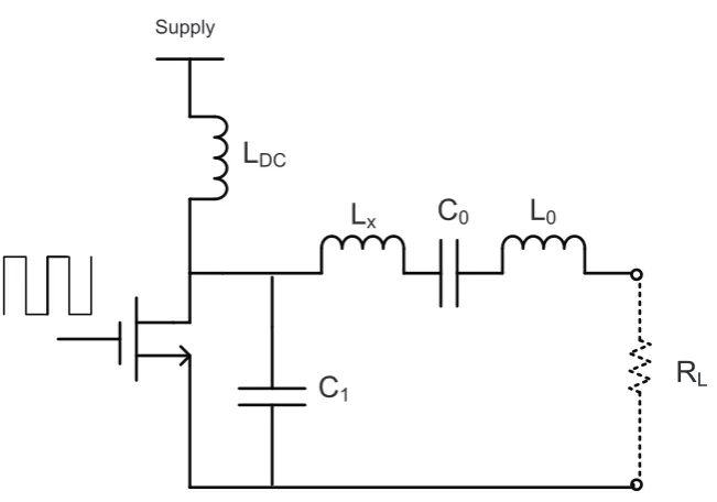
Class E Amplifier
Class E amplifier has a very simple circuitry as shown by Fig. 2.3. The key feature
of this structure is the addition of inductor, Lx in the output circuit [29]-[32]. The
inductance task is to null the effect of the parasitic capacitance, C1. Therefore
when the switch is closed, the voltage across the transistor has already fallen to zero
and no switching losses occur. This effect is known as the zero voltage switching
(ZVS) or soft switching. The capacitance in the output network helps to improve
the high frequency efficiency of the Class E PA compared to a Class D. However
under mismatched load conditions, the output voltage can be very high and ZVS
19
C
1 SupplyC
0L
0L
xL
DCR
LFigure 2.3: Schematic of a Class E PA.
2.2.4
A Practical Amplifier
In this section, practical measurements on GaN amplifier operating in a near switch
mode condition (between class C and E) is described. The work in this subsection
was performed by a colleague and presented in a joint publication [33].
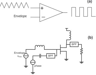
A simple way to obtain PWM operation is to use a comparator and a
trian-gular drive signal with the reference input controlled by the envelope modulation
(Fig. 2.4). In this work, the PWM signal is directly generated in the output power
device. The amplifier input is overdriven with sinusoidal carrier signal (Vp), and the
gate bias (Vbias) is controlled by the envelope component of the modulated signal.
Since the device threshold voltage (VT) is fixed, this has the effect of varying the
on/off duty cycle of the amplifier, as illustrated in Fig. 2.5. The method produces
two side effects, firstly the pulse width is no longer linear with respect to the
Envelope
+
_
BPF
BPF
Envelope vbias
phase
(a)
(b)
Figure 2.4: PWM generation:(a) ideal, (b) PA schematic
V
V
TV
biasV
pon
off
PWM DrainSignal
21
Transmission Line
RF Output
Vbias
RF Input
Figure 2.6: The PCB with the transmission line inductance and I/O ports indicated.
the PWM like signal at the drain of the device has a reduced slew rate because of
the limited gain of the device. This is particularly so for small conduction angles,
when conduction occurs at the peak of the sine wave. The device is operating more
like a class C amplifier in this region (conduction angles less than 50%). Efficiency
will not be as high as that of (Fig. 2.4).
The full amplifier including matching networks is implemented using surface
mount components on a standard FR4 printed circuit board (PCB), with double
sided copper layers as illustrated in Fig. 2.6. The inductor at the drain of the device
is implemented using a transmission line. The device is a CREE CGH40010 discrete
GaN high electron mobility transistor (HEMT) device suitable for high output power
(10 W). The carrier frequency was 395 MHz and a high-power input signal was used
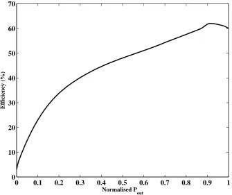
0 0.1 0.2 0.3 0.4 0.5 0.6 0.7 0.8 0.9 1 0
10 20 30 40 50 60 70
Normalised P out
Efficiency (%)
Figure 2.7: Efficiency against power output. PWM curve is for Vdd= 30 V. Pout is
normalised to peak output power of 39.6 dBm.
In Fig. 2.7, the plot shows the efficiency versus normalised output power for
both architectures. The power is normalised to the amplifiers peak output power;
in this case 39.6 dBm for Vdd = 30 V. The loss of efficiency at low output powers
is consistent with PWM operation, where slew-rate losses are essentially constant
whatever the pulse width (output power).
The peak to average power ratio (PAPR) of modern day modulations (CDMA/
OFDM) is between 6 dB and 8 dB [34] after crest factor reduction. Hence the
efficiency of the practical amplifier is much reduced with these signals. The average
23
about 35%. This is still a reasonable figure, compared to today’s amplifiers, but
there is still plenty of room for improvement.
The next sub-section will describe two amplifier architectures that remove the
need to modulate the pulse width of the drive signal. The amplifiers can be operated
at their highest efficiency all the time
2.2.5
Envelope Elimination and Restoration
A polar transmitter scheme which has been widely investigated over the years is
the EER which was first introduced by Kahn [35]. EER using switching amplifiers
can achieve high efficiency for complex modulation schemes such as OFDM. A basic
structure of EER is shown by Fig. 2.8. The input Cartesian signals are converted
to polar equivalents. A limiter is used to eliminate the envelope and produce a
constant amplitude phase modulated signal. The RF drive signal of the final output
stage contains that phase information. An envelope detector is used to extract the
amplitude information which is then amplified by a Class S amplifier and fed to the
final stage by means of supply modulation [35]-[37]. A problem associated with the
EER scheme is the delay mismatch between the amplitude and phase components
which can lead to serious spectral expansion at the output [38]. A possible solution to
avoid the time mismatch between the two paths is to delay the phase component [39].
Another major drawback of this scheme is the bandwidth expansion that is
produced when the input signal is converted to polar. The Class S amplifiers have
difficulties in tracking quickly changing voltages and are normally required to have
Envelope Detector
Phase
S
E DC supply
Modulator
High Power Amplifier Input
Signal
Local Osc.
Figure 2.8: An EER transmitter architecture.
bandwidths put immense strain on the supply modulators.
Hole punching has been proposed as a possible solution to the polar bandwidth
expansion problem. The idea behind the approach is to prevent the zero
cross-ings of the Cartesian components by establishing a boundary [41]. Thus the phase
components do not experience any rapid transition which normally requires a wide
bandwidth to capture resulting in bandwidth expansion [27]. The hole punching
technique leads to the generation of minimal adjacent channel power. However,
substantial in-band distortion is produced leading to degradation in error vector
magnitude (EVM). We quantify the trade-off between EVM and bandwidth
expan-sion in [42].
At this stage, EER scheme is appropriate for input signals with limited envelope
dynamic range and lesser bandwidth expansion such as π4 shift quadrature
phase-shift keying (QPSK) or Gaussian minimum phase-shift keying (GMSK) [40]. However,
these narrowband modulation schemes are not appropriate for upcoming wireless
25
Signal source
Signal Component
Separator
Modulator
Modulator
P
A
P
A Power
Combiner
Figure 2.9: A LINC transmitter architecture.
2.2.6
LINC Transmitter Architecture
The amplification of amplitude-varying signals by non-linear SMPAs normally give
rise to distortions. The distortions are generally intermodulation components of the
signal and the intermodulation products are present both in-band and out-of-band.
Linear amplification of non linear components (LINC) is a method used to
am-plify signals with varying amplitudes using non-linear amplifiers without degradation
by non-linear SMPAs [43]- [49].
Fig. 2.9 shows the operation of the LINC system. The signal component
sep-arator decomposes the original signal into two constant amplitude phase varying
signals. The two signals are then amplified by highly efficient but non-linear
am-plifiers such as Class D or E. The last stage is the combining stage where the two
signals constructively or destructively interfere to produce an amplified version of
the input signal.
In [50], we characterise the LINC performance of a Class E amplifier. Traditional
LINC analysis does not apply for a Class E amplifier since Class E is neither an ideal
voltage nor current source. We propose a load-pull analysis to obtain its transfer
to characterise any amplifier class in a LINC scheme. Simulations using advanced
design system (ADS) showed an efficiency of 81% was achievable when the Class E
amplifier was operated in the LINC scheme. It was also found that switching losses
account for more that 60% of the total losses.
Moreover, the practical implementation of LINC is not an easy task. The system
is very susceptible to disparity in phase, delay and amplitude. It is therefore nearly
impossible to achieve a perfect constructive or destructive recombination.
The goal of the thesis is to come up with an all digital drive circuit for SMPAs
such as those discussed in this section (Section 2.2). As previously indicated in
Sec-tion 1.5 synchronous digital circuits will produce quantisaSec-tion noise. Σ∆ techniques
can control the noise spectrum and will be discussed in the next section.
2.3
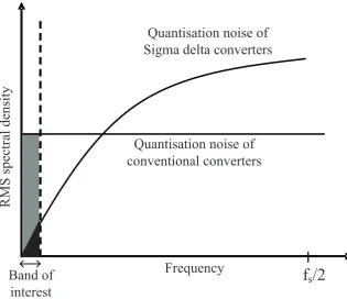
Sigma Delta Modulators
The Σ∆ technique has been in existence for many years but recent technological
advances have made it more widespread. Σ∆ modulators use noise shaping and
oversampling techniques to limit quantisation noise in the band of interest. The
oversampling ratio of the Σ∆ modulator (OSRΣ∆) needs to be much greater than
one. The oversampling technique allows an input signal to be sampled in such a
way that two adjacent samples are very similar. The error generated by the coarse
quantiser will thus have a high degree of correlation. Hence the quantisation error
can be predicted and subtracted from the data through a feedback loop. This process
27
Quantisation noise of
Sigma delta converters
Quantisation noise of
conventional converters
f
s/2
R
M
S
s
p
ec
tr
al
d
en
si
ty
Band of
interest
Frequency
Figure 2.10: Showing the difference between conventional converters and Σ∆ con-verters. fs is the Σ∆ sample rate.
shows the reduction in quantisation noise when using a Σ∆ converter compared
to a conventional converter. The concept of Σ∆ modulation has contributed to
the improvement of many components (such as high performance analog to digital
converters (ADCs) and digital to analog converters (DACs)) leading to a higher
degree of integration enjoyed by current wireless transceivers.
2.3.1
Linear
Σ∆
Model
A basic lowpass Σ∆ model can consist of a subtraction node, a discrete-time
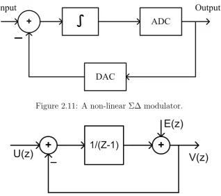
integra-tor and a quantiser as shown in Fig. 2.11. An integraintegra-tor is used in this architecture
+
䌿
ADC
DAC
Input
Output
_
Figure 2.11: A non-linear Σ∆ modulator.
1/(Z-1)
+
+
E(z)
V(z)
U(z)
_
Figure 2.12: A linear z-domain model of a Σ∆ modulator.
noise at baseband. The integrator provides an infinite gain at DC. A Σ∆
modu-lator is considered to be both non-linear and dynamic because of the presence of
the quantiser and the integrator respectively. The Σ∆ modulator is normally
lin-earised to ease the mathematical analysis. The quantiser can be approximated to a
white additive noise source,E(z), provided it satisfies a few criteria [54]. One of the
most significant criteria is that the input signal needs to be sufficiently small and
thus never overloads. A linear z-domain model of the a lowpass Σ∆ is depicted in
Fig. 2.12. The linear z-domain model can be further simplified as shown in Fig. 2.13.
The integrator which has a transfer function of z−11 is replaced by a two loop
29
Z
-1Z
-1+
+
+
E(z)
U(z)
Y(z)
V(z)
_
Figure 2.13: A linear z-domain model of a MOD1 [51] Σ∆ modulator.
analysing Fig. 2.13.
Y(z) =z−1Y(z) +U(z)−z−1V(z). (2.1)
V(z) = Y(z) +E(z),
=z−1Y(z) +U(z)−z−1V(z) +E(z),
=U(z) + (1−z−1)E(z). (2.2)
V(z) =ST F(z)U(z) +N T F(z)E(z). (2.3)
For further simplification, the terms signal transfer function (STF) and noise transfer
function (NTF) are introduced. The STF is unity and therefore no filtering occurs.
The NTF is 1−z−1and the noise is high pass filtered. The characteristic of the NTF
can be further illustrated by the use of a pole-zero diagram. The zeros of the NTF
are located on the unit circle at DC as shown in Fig. 2.14 causing the quantisation
X
Real axisImaginary axis
Figure 2.14: Pole/zero diagram of a lowpass Σ∆ modulator.
The square of the magnitude of the NTF in the frequency domain is calculated
in order to estimate the in-band power of the quantisation noise as shown below.
N T F(ejω) = (1−e−jω)2,
= (1−cosω−jsinω)2,
= 2−2cos(ω),
= 4sin2(πf). (2.4)
N T F = (2sin2(πf))2. (2.5)
When f = 0, the NTF given by (2.5) is also zero. The NTF grows as frequency
increases. This causes the noise to increase and is a potential source of interference
to adjacent channels. It is quite clear from (2.5) that the quantisation noise is filtered
away from DC. This is a highly desirable feature as in a lowpass Σ∆ configuration,
31
−40 −35 −30 −25 −20 −15 −10 −5 0
45 50 55 60 65 70 75 80 85 90 95
Signal Power (dB)
SQNR (dB)
Simulation result Theoretical result
Figure 2.15: A plot showing the SQNR with varying signal power (urms=1) for
MOD-1 Σ∆ with output levels +1,-1. The input signal is a sine wave.
2.3.2
Derivation of Signal to Quantisation Noise Ratio for
MOD1
Σ∆
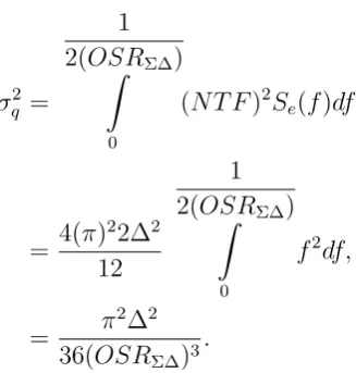
As mentioned earlier in this chapter, the quantisation error is treated as a white
additive noise. The noise power, σ2
e, is given by ∆2
12 where ∆ is the step size of the
linear quantiser [51]. The one-sided power spectral density, Se(f), is given by 2σe2
(where the sample rate has been normalised to unity). The in-band noise power,
σ2
q, in the output is given by integrating the product of Se(f) and the NTF given
which is given by 2(OSR1
Σ∆).
σ2q =
1 2(OSR∫ Σ∆)
0
(N T F)2Se(f)df,
= 4(π)
22∆2
12
1 2(OSR∫ Σ∆)
0
f2df,
= π
2∆2
36(OSRΣ∆)3
. (2.6)
In this derivation, the step-size, ∆, of a 1-bit quantiser is assumed to be 2 [51].
σq2 = π
2
9(OSRΣ∆)3
. (2.7)
The peak amplitude of a sine wave is denoted by Am. Since the STF is unity, the
output signal power is given by
σ2u = (Am)
2
2 . (2.8)
The signal to quantisation noise ratio (SQNR) is the relationship between the signal
and the quantisation noise. The SQNR for a MOD-1 lowpass Σ∆ is given by
SQN R= σ
2 u σ2 q
= 9(Am)
2(OSR Σ∆)3
2π2 . (2.9)
Fig. 2.15 shows plots of input power against SQNR. The figure contains a theoretical
plot obtained from (2.9) and a simulated plot. The simulated curve follows the
theo-retical curve except for large values of input power. When the input power lies near
the quantiser range boundary or is excessively high, the quantiser overloads. This
33
0 0
Quantiser Input
Q
u
a
n
ti
se
r
O
u
tp
u
t
Figure 2.16: Quantiser input and output of a 4-bit uniform quantiser (thin lines) and a 3-bit non-uniform quantiser (thick lines).
increase in the difference between the theoretical and simulated SQNR is expected.
2.3.3
Non-Uniform Quantisation
A uniform quantiser is appropriate for signals with uniform distribution. However,
signals with non-uniform probability density function (PDFs) require non-uniform
quantisers for optimum quantisation. The input range is divided in unequal
inter-vals. Depending on the PDF of the input signal, the threshold levels of the quantiser
can be more densely located for some values of the input signals and more coarsely
+ + + + Q
Z-1 Z-1
Z-1
_ _
U Y V
Figure 2.17: A linear z-domain model of a MOD-2 Σ∆ modulator.
In [56]-[58], non-uniform quantisers are used for input signals which can be
ap-proximated to Gaussian signals. Since such a signal is more likely to have small
amplitudes, the quantiser is designed to have smaller quantisation steps around
that region. For uncommon larger input values, the quantisation steps are larger.
Fig 2.16 shows a non-uniform quantiser (3-bit) superimposed on a uniform one
(4-bit). SQNR results in [56] show that the 3-bit non-uniform quantiser outperforms
the 3-bit uniform quantiser. It is also shown that the 3-bit non-uniform quantiser
and a 4-bit uniform quantiser produce similar SQNR results.
2.3.4
Higher Order
Σ∆
Converters
Higher order converters can be used to obtain a better noise shaping effect. They
are designed by cascading the MOD-1 architectures discussed in earlier paragraphs.
Fig. 2.17 shows a second order Σ∆ modulator(MOD-2 [51]) which is essentially a
MOD-1 Σ∆ with an additional integrator and another feedback path.
The SQNR is improved by the new NTF. However, the improved noise shaping
characteristics of the higher order Σ∆ are achieved at the expense of increased
35
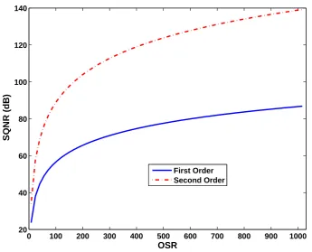
0 100 200 300 400 500 600 700 800 900 1000
20 40 60 80 100 120 140
OSR
SQNR (dB)
First Order Second Order
Z
-2Z
-2+
+
+
E(z)
U(z)
Y(z)
V(z)
_
Figure 2.19: A linear z-domain model of a bandpass Σ∆ modulator.
X Real axis
Imaginary axis
Real axis
X
Imaginary axis
(a) (b)
Figure 2.20: Pole/zero diagram of the NTF of (a) first-order lowpass and (b) second-order bandpass Σ∆ modulator.
additional pressure on the output bandpass filters.
The SQNR can also be further increased by increasing OSRΣ∆. Fig. 2.18 shows
the improvement in SQNR as OSRΣ∆ increases for MOD-1 and a MOD-2
archi-tectures. It can be observed that a higher OSRΣ∆ is needed to achieve the same
SQNR in MOD-1 compared to MOD-2, making MOD-2 a more practical choice as
37
Bandpass !
Modulator Bandpass
Filter Class S
Amplifier RF
Signal Input
Output
c sbp
f
f
4
@
f
cFigure 2.21: A bandpass Σ∆ architecture.
2.3.5
Bandpass
Σ∆
Modulators
Analysing lowpass Σ∆ is essential to understand the concept of Σ∆. However,
lowpass Σ∆ applies to signals at DC. Signals at radio frequencies are needed for most
communication systems. For a bandpass modulator, the highpass characteristic
of the NTF has to be replaced by the bandstop transfer function [59]-[61]. The
most common method to design a bandpass Σ∆ modulator is to perform a simple
mathematical transformation on a suitable lowpass Σ∆. It is called a DC to fsbp/4
transformation and it requires the z−1 in the transfer function to be replaced by
−z−2 [51]. f
sbp is the sampling rate of the bandpass Σ∆. Fig. 2.19 shows the linear
z-model of a MOD-2 bandpass Σ∆.
The number of zeros in the NTF of the lowpass Σ∆ is doubled and the zeros
are rotated in the z-plane from z = 1 to z = j as illustrated by Fig. 2.20. In
the frequency domain, the noise suppression region shifts from DC to fsbp/4. The
system block diagram of a bandpass Σ∆ is shown in Fig. 2.21.
Fig. 2.22 shows the spectrum plot of a 20 MHz OFDM signal after it has been
modulated by a fourth-order bandpass Σ∆ converter. The null is no longer at DC, it
0 200 400 600 800 1000 1200 1400 1600 1800 2000 −35
−30 −25 −20 −15 −10 −5 0
Frequency (MHz)
Spectrum (dB)
Figure 2.22: Spectrum of the output of a bandpass Σ∆. fsbp=4 GHz, fc= 1.024
GHz, OFDM input signal level= -12 dB (urms=1).
noise in the two immediate adjacent channels are calculated and given by ACP(1)
which is -23.7 dB and ACP(2) which is -30.4 dB. The ACPs are defined as the noise
power in the adjacent channel divided by the signal power. This bandpass Σ∆ is a
few dB short of the WLAN specification.
The next section will show how Σ∆ can be used in upconverter circuits for
SMPAs.
2.4
Sigma Delta-Based Transmitter Architectures
Σ∆ waveforms are generally of the ‘on’/‘off’ type. Such signals can be used to
![Figure 1.1: Evolution of wireless technologies (after [2]).](https://thumb-us.123doks.com/thumbv2/123dok_us/7944397.1318677/24.595.135.473.107.342/figure-evolution-of-wireless-technologies-after.webp)