Available online:
https://edupediapublications.org/journals/index.php/IJR/
P a g e | 1241Multi-Input RES Based Interleaving High Frequency Bidirectional
Transformer less Inverter
D.SABITHA
K.SURESH
M. Tech Student
Associate professor
Department of PEED
Department of EEE
HITAM Engg College
HITAM Engg College
ABSTRACT
A New Multi-Input Transformerless Photo voltaic inverter with bidirectional capability has been developed where the concept of High Frequency Leg (HFL) is used. This allows the use of high switching frequency which reduces the size of the filter elements. As the number of legs is increased, the power handling capacity of the inverter is increased and the inductor current ripple is reduced. The bi directional feature of this inverter has made it more attractive for PV applications.
Keywords- Basic Switching Cells, Photovoltaic Inverters without Isolation Transformer, Bidirectional power flow, High Frequency Leg
I. INTRODUCTION
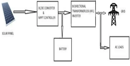
Generally, the solar based power systems consist of PV panel, battery, inverter, load or grid. The solar panel produces the DC power during the sunshine hours. The excess power generated is stored in batteries but these batteries add the recurring cost. The DC power is converted to AC with the help of inverter. The AC is then fed into the grid, from where it can be used for the domestic, commercial and industrial applications. During the non-sunshine hours, the user relies upon the batteries. When both panel and battery doesn’t work, the bidirectional inverter charges the battery from the energy supplied by the grid.The PV generating system is shown in Fig.1.
Fig. 1. Block diagram of PV Generating System
To provide a short circuit current path on the DC side carrier-based modulation technique has been
used in [1] to magnetize the inductor after every operation mode. The photo-voltaic inverter with no transformer for isolation has become more attractive due to higher efficiency and lower weight. However, the problem is DC offset current which is critical to the power system [2]. To construct a general series and parallel grid-interfacing system, two four leg three-phase inverter circuit together with DC micro-sources and non-linear loads are employed [3]. A single phase series-connected inverter is used to interconnect AC loads with the micro-grid. The control strategy is designed to stabilize the load voltage irrespective of the grid voltage magnitude as well as transfers a specific amount of renewable source based power to the load. Besides, the inverter is forced to operate at leading power factor irrespective of the power factor of the load. To track as well as eliminates the harmonics in the load voltage, a nonlinear Spatial Repetitive Controller (SRC) is used which facilitates the control strategy. The controller is implemented based on position domain of the fundamental micro grid phase angle [4]. Two basic switching cells, the P-NPCC (Positive Neutral Point Clamped Cell), and the N-NPCC (Negative Neutral Point Clamped Cell) for the grid-tied inverter topology generation is used to build NPC topologies. A family of single phase transformer less full-bridge NPC inverter topologies based on the basic switching cell is derived with low leakage current. The (Positive Negative-NPC) PN-NPC topology has the following advantages and evaluated by experimental results. 1) The common-mode voltage is clamped to a constant level, so the leakage current can be well suppressed effectively. 2) The excellent differential mode characteristic is achieved like the isolated full-bridge inverter with unipolar SPWM. 3) The PN-NPC topology features the best conversion efficiency [5].
Available online:
https://edupediapublications.org/journals/index.php/IJR/
P a g e | 1242inverters. The complexity is reduced and it improves the
reliability of the system.
The Transformer less inverters are checked for the presence of leakage current, to ensure safety.The magnitude of leakage current depends upon the common mode voltage. The common mode voltage is defined as the voltage of equal magnitude and phase component appearing in both the lines of the 2 wire cable. One way of eliminating the common mode voltage is the use of inductor in the bifiliar winding which will eliminate the higher frequency common mode signals.
In order to overcome the drawbacks of conventional inverters, the bi directional Transformer less inverter is proposed which has the following features that increases the power handling capacity of the inverter. The features are:
1.
The shoot-through fault is eliminated, whichincreases the reliability.
2. The leakage current due to common mode
voltage is reduced, due to the use of inductor in the bifiliar windings.
3. MOSFET switches are employed, as they
operate at high switching frequency. Also they have low conduction and switching losses, which improves the overall efficiency of the system. The size of the filter elements is reduced considerably as they are operated at high switching frequency.
4. Depending upon the demand, the inverter
capacity can be increased by adding extra legs (HFL) in the circuit.
5. The most important feature is the bi directional
power handling capacity, where it works as inverter when power flows from panel to grid and as the rectifier when the power flows from the grid to the battery.
II.HIGH FREQUENCY LEG CONCEPT OF
PROPOSED SYSTEM
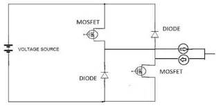
A. Basic Switching Cells
The switching cells are combined to form power electronic circuits. Each cell is made up of a
controllable switch (MOSFET,IGBT) and an
uncontrolled diode in series to it. It has got three terminals: (+) connected to the source positive, (-) connected to the negative of source and the third terminal at the junction of the two switches which allows
bi directional power flow. By using the switching cells in the power electronic circuit, the shoot- through fault is eliminated.The basic switching cells are shown in Fig.2.
Fig. 2. The basic Switching Cells
The P-cell and N-cell can be connected in parallel to form a phase leg of the bi directional inverter. The advantage of using the above parallel leg in comparison to the conventional IGBT with an anti-parallel diode is that the dead time required between the switching of any two cells is eliminated. Even the IGBT – diode can be used for the construction of parallel leg of the inverter, it is not generally preferred as the IGBT switches have high switching losses.
B. MOSFET in HFL Technique
The MOSFET switches are used as they do not suffer from reverse body recovery. The operating frequency is high compared to IGBT switches. The switching losses of the MOSFET switches are relatively low compared to that of IGBT switches. The MOSFET switches used for the construction of the parallel leg is shown in Fig.3.
Fig. 3 Parallel Combination Of legs
In this paper, IGBT switches are replaced by MOSFET switches which has better switching performance. The multiple legs of the bridge are integrated and the switches are turned on with high-frequency control signals, hence efficiency is improved.
III.CONVENTIONALTRANSFORMER LESS PHOTOVOLTAIC INVERTERS
Available online:
https://edupediapublications.org/journals/index.php/IJR/
P a g e | 1243Bridge Inverter. The advantage of this inverter is that the
leakage current is eliminated, but the drawback is the shoot-through fault. The
drawback with Highly Efficient and Reliable Inverter Concept converter (HERIC) topology is the use of more semiconductors and its reactive power incapability. The disadvantage of H5 inverter structure is the higher conduction losses [6-9].
IV. PROPOSED BIDIRECTIONAL
TRANSFORMERLESS INVERTER.
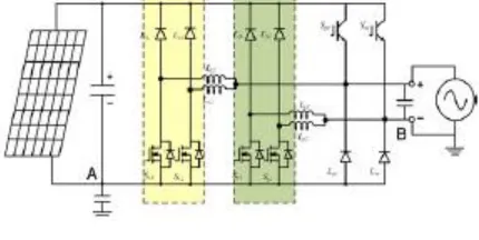
The proposed Inverter topology consist of N-cell legs and P-cell legs. The number of N cell legs with separate inductors are integrated to form a single leg. The N-Cell leg is made up of upper diode and lower MOSFET in series to it. The P-cell leg is made of the upper IGBT switches without antiparallel diode and the lower diode which is connected in series. There are totally eight inductors used. The grid voltage directions are selected by the P-cell legs. The third terminal of the first P-cell leg is connected with the positive port of grid side and the negative N-cell comprising of the inductors Ln1,Ln2,Ln3 and Ln4. Similarly the third terminal of the second P-cell leg is connected to the negative of the grid side and to the N-cell with inductors Lp1,Lp2,Lp3 and Lp4. The circuit diagram of the proposed system is shown in Fig.4.
The switches Snf and Spf are operated at inverter mode while the diodes are active during the storage mode.
Fig.4. Circuit Diagram
The proposed inverter topology operates in two modes of operation such as PV mode and storage mode.
A. PV mode(Inverter mode)
In this mode of operation, the switches Spf,Snf are active. Since there is no parallel diode in IGBT, the dead time requirement is reduced. During the positive half cycle, the switch Spf is turned on, where the switches Sp1,Sp2,Sp3 and Sp4 are controlled by the gating signals. During the negative half cycle, the switch Snf is turned on, which controls the firing of Sn1,Sn2,Sn3 and Sn4.
Inorder to reduce the current ripple at the AC side, the carrier signal during the negative half cycle is given a phase shift of 180 degree. The Interleaving modulating technique is shown in Fig.4(a).
Fig. 4(a). Modulating Technique
The reference wave is compared with the carrier and the outputs are generated for the P-cell switches. The carrier is phased shifted by 180 degree and is compared with the reference wave. The outputs generated from the later comparison are used as the gating signals for the N-cell switches.The modulating signals based on the above modulating circuit is shown in Fig.4(b).
Fig.4(b). PWM Generated Signals
There are four modes of operation. In the first mode of PV mode, all the four switches are turned on. The voltage across the inductor is increasing steadily. In the second mode of PV mode, two switches(Sp2,Sp4) are turned
on, the voltage across the inductor decreases. The free wheeling path is provided by the diode Dp1,Dp3. In the third
Available online:
https://edupediapublications.org/journals/index.php/IJR/
P a g e | 1244Fig.5. Operating modes in PV mode
B. Storage Mode (Rectifier Mode)
In this mode of operation, the diodes Dpr,Dnr play an important role whereas the switches Spfand Snfare turned off. Similar to the previous operating mode, the storage mode also has got four operating modes. Even during this mode of operation, all the features of the proposed system are achieved.
The operation can be explained as follows. During the first interval, the diode Dnr is turned on, and the
Available online:
https://edupediapublications.org/journals/index.php/IJR/
P a g e | 1245Fig.6. Operating modes in Storage mode
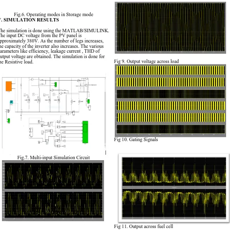
V. SIMULATION RESULTS
The simulation is done using the MATLAB/SIMULINK. The input DC voltage from the PV panel is
approximately 380V. As the number of legs increases, the capacity of the inverter also increases. The various parameters like efficiency, leakage current , THD of output voltage are obtained. The simulation is done for the Resistive load.
Fig.7. Multi-input Simulation Circuit
Fig 8. Current across Lp1, Ln1 inductors waveform
Fig 9. Output voltage across load
Fig 10. Gating Signals
Fig 11. Output across fuel cell
VI. CONCLUSION
Available online:
https://edupediapublications.org/journals/index.php/IJR/
P a g e | 1246is attractive for PV application. In this paper, the
comparison between the bi directional inverter with 2 and 4 legs has been done by simulating the circuits in MATLAB.
ACKNOWLEDGEMENT I am thankful to my project guide and my Institution for their valuable support and suggestions during my project work.
REFERENCES
i. ALAJMI, B.N., AHMED, K.H., ADAM, G.P., WILLIAMS, B.W.,
―SINGLE-PHASE SINGLE-STAGE TRANSFORMER LESS GRID-CONNECTED PV SYSTEM,‖ IEEE TRANS. POWER ELECTRON., VOL.28, NO.6, PP.2664-2676, JUNE 2013.
ii. Guofeng He, Dehong Xu, Min Chen, ―A Novel Control
Strategy of Suppressing DC Current Injection to the Grid for Single-Phase PV Inverter‖ IEEE Trans. Power Electron., vol.30, no.3, pp.1266-1274, March 2015.
iii. W. Fei, J. L. Duarte, and M. A. M. Hendrix, ―Grid-interfacing converter systems with enhanced voltage quality for microgrid application-concept and implementation,‖ IEEE Trans.
Power Electron., vol. 26, no. 12, pp. 3501–3513, Dec. 2011. iv. S. Dasgupta, S. K. Sahoo, S. K. Panda, and G. A. J. Amaratunga, ―Single phase inverter-control techniques for interfacing renewable energy sources with micro grid—Part II: Series-connected inverter topology to mitigate voltage-related problems along with active power flow control,‖ IEEE Trans. Power Electron., vol. 26, no. 3, pp. 732–746, Mar. 2011
v. L. Zhang, K. Sun, L. Feng, H. Wu, and Y. Xing, ―A family of neutral point clamped full-bridge topologies for transformer less photovoltaic grid-tied inverters,‖ IEEE Trans. Power Electron., vol. 28, no. 2, pp. 730–739, Feb.2013.
vi. S. B. Kjaer, J. K. Pedersen, and F. Blaabjerg, ―A review of single-phase grid-connected inverters for photovoltaic modules,‖ IEEE Trans. Ind. Appl., vol. 41, no. 5, pp. 1292–1306, Sep. 2005.
vii. R. Gonzalez, J. Lopez, P. Sanchis, and L. Marroyo, ―Transformer less inverter for single-phase photovoltaic systems,‖ IEEE Trans. Power Electron.,vol. 22, no. 2, pp. 693– 697, Mar. 2007.
viii. S.M.Araujo, P. Zacharias, and R. Mallwitz, ―Highly efficient
single-phase Transformer less inverters for grid-connected photovoltaic systems,‖ IEEE Trans. Ind. Electron., vol. 57, no. 9, pp. 3118–3328, Sep. 2010.
ix. Y. Xue, L. Chang, S. B. Kjaer, J. Bordonau, and T. Shimizu, ―Topologies of single-phase inverters for small distributed power generators: An overview,‖ IEEE Trans. Power Electron., vol. 19, no. 5, pp. 1305–1314, Sep. 2004.
AUTHOR DETAILS:
D.SABITHA
Received B.Tech degree from ADAMS College of
engineering, Palvancha, Khammam, Telangana in
2005. And currently pursuing M.Tech in Power
Electronicsand Electrical Drives at Hyderabad
Institute
of
Technology
And
Management,
Gowdavelly,
Medchal,
Ranga
Reddy,
and
Telangana. Her area of interest is in Electrical
inspection field.
K.SURESH
Available online:
https://edupediapublications.org/journals/index.php/IJR/
P a g e | 1247Electrical circuits. He is having 13 years of teaching
experience.