University of South Carolina
Scholar Commons
Theses and Dissertations
2017
High Quality Low Offcut 4h-Sic Epitaxy and
Integrated Growth of Epitaxial Graphene for
Hybrid Graphene/Sic Devices
Anusha Balachandran
University of South Carolina
Follow this and additional works at:https://scholarcommons.sc.edu/etd
Part of theElectrical and Computer Engineering Commons
This Open Access Dissertation is brought to you by Scholar Commons. It has been accepted for inclusion in Theses and Dissertations by an authorized administrator of Scholar Commons. For more information, please [email protected].
Recommended Citation
Balachandran, A.(2017).High Quality Low Offcut 4h-Sic Epitaxy and Integrated Growth of Epitaxial Graphene for Hybrid Graphene/Sic
H
IGH QUALITY LOW OFFCUT4H-S
IC
EPITAXY AND INTEGRATED GROWTH OFEPITAXIAL GRAPHENE FOR HYBRID
G
RAPHENE/S
IC
DEVICESby
Anusha Balachandran
Bachelor of Engineering
Government College of Technology, Coimbatore, 2013
Submitted in Partial Fulfillment of the Requirements
For the Degree of Doctor of Philosophy in
Electrical Engineering
College of Engineering and Computing
University of South Carolina
2017
Accepted by:
MVS Chandrashekhar, Major Professor
Tangali S. Sudarshan, Committee Member
Simin Grigory, Committee Member
Andrew B. Greytak, Committee Member
DEDICATION
ACKNOWLEDGEMENTS
First and foremost, I owe my deepest gratitude to my advisor Dr. MVS
Chandrashekhar, who has been supportive throughout my PhD by his insightful
suggestions and advisement. I owe my deepest gratitude to my committee member and
my mentor Prof. T.S. Sudarshan for being instrumental in motivating and encouraging
me by his research expertise and stimulating discussions throughout my research. I would
to thank the rest of my thesis committee: Prof. Simin Grigory and Dr.Greytak for their
thoughtful comments and motivation for improving this work.
I am indebted to my research group members for many stimulating discussions.
Particularly, Dr. Haizheng Song for being my mentor during the initial days of my PhD
and training me with the laboratory equipments. I would also like to thank all my past
and present colleagues in the Clean Energy Lab: Omar, Shamaita, Kevin, Joey, Hani,
Surya, Ifat, Josh and Ken for all their help and healthy discussions during my reasearch. I
would like to say my special thanks to Mr. Metts of Electrical Engineering department
for being a constant source of support and helping me with the lab equipments.
I am forever grateful to my late uncle Vembu Subramanian for encouraging me to
consider USC in the first place. Last, but not the least, I would like to thank my parents,
my brother and my fiancé Venkat for their moral support without whom this PhD would
not have been successful. I would like to convey my heartfelt thanks to my dear
ABSTRACT
Power electronic semiconductor devices are critical components in
next-generation power systems such as hybrid electric vehicles and smart grid power controls
enabling reduction in system size, weight, and cost. Wide bandgap materials such as SiC,
GaN, and diamond have been investigated to replace silicon, due to their superior
material properties. Of these, 4H-SiC is considered the most viable candidate beyond
3kV due to its technological maturity, its wide band gap (3.23 eV), high breakdown field
(4×10⁶ V/cm), high thermal conductivity (5 W/cm/K) and, more importantly, its indirect
bandgap.
The main contribution of my research relates to the development and
investigating the methods for growing high-quality SiC homoepitaxial layers with low
defect density, particularly basal plane dislocations (BPDs) which severely affects the
SiC bipolar device yield in high scale environments. The first approach of eliminating
BPDs was to produce high quality SiC epilayers using a novel Si precursor
Tetrafluorosilane (TFS) on nearly on-axis substrates (0.5° offcut) which inherently
suppress BPD formation, by identifying a unique growth regime that promotes step flow
growth in a nearly on-axis surface which is considered a major challenge in SiC epitaxy.
As an alternate solution to BPD elimination in the most common 4º subtsrtaes, we
developed a composite growth structure to produce 100% BPD free SiC epilayers over a
Final part of this work is integrating the high quality SiC epilayers for fabricating
hybrid EG/SiC Schottky structures with epitaxial graphene as an in-situ high temperature
metal contact grown using TFS under Argon ambience. The EG/SiC Schottky devices
fabricated exhibited an excellent ideality of 1.1 and a barrier height of 0.85 eV. These
EG/SiC Schottky devices were tested as photodetectors for sensing UV light owing to
graphene’s transparent optical property and 4H-SiC bandgap which is in the range of UV
spectrum.
With these contributions made towards increasing the material quality and yield
of SiC and SiC-graphene devices, SiC can be envisioned as a versatile and reliable
material for power electronics and harsh environment sensor applications in the near
TABLE OF CONTENTS
Dedication ... iii
Acknowledgements ... iv
Abstract ...v
List of Tables ... ix
List of Figures ...x
Chapter 1: Silicon Carbide ...1
1.1 Introduction ...1
1.2 SiC properties...2
1.3 SiC epitaxial growth methods ...8
1.4 Step controlled SiC epitaxy ...14
1.5 Structural defects in SiC ...22
1.6 State of the art SiC wafer and device technology ...27
Chapter 2: Homoepitaxial growth of 4H-SiC using halogenated precursors ...28
2.1 Introduction ...28
2.2 Comparative study between DCS and TFS precursors ...30
2.3 Parasitic deposition and growth rate comparison ...32
2.4 Growth rate vs. C/Si ratio ...35
2.5 Unintentional net doping control vs. C/Si ratio ...37
Chapter 3: Epitaxial growth on nearly on-axis (0.5˚) 4H-SiC substrates using TFS ...43
3.1 Introduction ...43
3.2 Experimental setup...50
3.3 High quality nearly on-axis epitaxial growth using TFS ...51
Chapter 4: Basal plane dislocations (BPD) free 4 4H-SiC epilayers using DCS ...63
4.1 Introduction ...63
4.2 Novel composite growth structure for BPD free active device layers ...68
4.3 Experimental details...70
4.4 Buffer epilayer growth and eutectic etching ...71
4.5 Recombination layer growth ...74
Chapter 5: Integrated epitaxial graphene growth on 4H-SiC using TFS ...81
5.1 Introduction ...81
5.2 Previous work on epitaxial graphene (EG) growth using TFS ...86
5.3 Temperature ramp down study of EG growth using TFS ...91
References ...106
LIST OF TABLES
Table 1.1 Properties of various semiconductor materials ...3
Table 2.1 Free formation energy (kcal/mol) for various SiC etching reactions calculated from JANAF thermochemical data ...37
Table 2.2 Defect densities on epilayers grown using DCS or TFS ...42
LIST OF FIGURES
Figure 1.1 Tetrahedral basic unit of SiC ...4
Figure 1.2 ABC sites in hexagonal crystal lattice ...4
Figure 1.3 Stacking arrangements seen along [112̅0] direction of SiC polytypes ...6
Figure 1.4 Hexagonal unit cell of SiC showing different crystal planes ...7
Figure 1.5 Lely process for SiC bulk growth ...8
Figure 1.6 Schematic of a seeded sublimation (SE) or PVT growth reactor ...9
Figure.1.7 Schematic of (a) cold-wall reactor, (b) hot-wall reactor configuration ...12
Figure.1.8 Crystal growth initiated by a screw dislocation on an ideal on-axis surface ....14
Figure.1.9 4H-SiC crystal showing offcut plane towards [112̅0] direction ...15
Figure.1.10 Schematic representation of the growth mechanism on (a) well-oriented and (b) off-oriented of 6H-SiC [0001] faces ...17
Figure.1.11 Surface processes involved on a stepped surface with unit step height h and terrace length 𝜆0 ...18
Figure.1.12 Schematic of a stepped surface showing regular array of steps and step bunching ...20
Figure.1.13 Optical microscopy image of SiC epilayer surface showing defects and their effects on the device performance ...23
Figure.1.14 Schematic of a stacking fault seen in 4H-SiC due to the slip in basal plane (0001) ...26
Figure 2.1 Schematic diagram of the CVD furnace used for SiC growth ...31
Figure 2.2 SiC-CVD epitaxial growth recipe using TFS/DCS Si precursor ...32
Figure 2.4 CVD furnace geometry and temperature distribution simulated using Virtual Reactor ...33
Figure 2.5 Deposition on injector tube (split) and Injector cap (funnel) (bottom view) for 1 hour growth with 10 sccm DCS or TFS. (a) and (d):before growth; (b) and (e): after DCS-growth; (c) and (f): after TFS-growth ...34
Figure 2.6 Temperature versus Gibbs free energy of thermal decomposition reactions of SiH4, SiH2Cl2 and SiF4 ...35
Figure 2.7 Growth rate vs. C/Si ratio for for DCS and TFS-growths at different flow rates (Trend lines shown are guide to eyes) ...36
Figure 2.8 (a) Net doping concentration vs. C/Si ratio for (a) TFS (at 10 sccm), (b)TFS (at 5 sccm) and (c) DCS (at 5.6 sccm) growths ...38
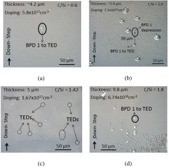
Figure 2.9 NOM pictures of growth samples, (a)&(b) DCS C/Si=0.6,C/Si=1.8, (c)&(d) TFS C/Si=0.6,C/Si=1.8 ...40
Figure 2.10 Epilayer RMS roughness vs. C/Si for DCS, TFS growths (Trend lines shown are guide to eyes) ...41
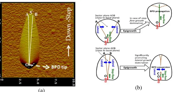
Figure 3.1 Basal Plane Dislocation (screw and mixed (60) dislocation) showing their burgers vector along {1120} directions in the crystal lattice ...45
Figure 3.2 a) BPD conversion and propagation and b) Quasi on-axis surface showing BPD to TED conversion due to increase in WBPD ...47
Figure 3.3 On-axis growth results using TFS (5 sccm) (a) Rg vs. C/Si ratio curve, (b)
Unintentional doping concentration vs. C/Si ratio curve (trend lines shown in 1.(a) & (b) are guide to the eyes) ...52
Figure 3.4 Schematic of important growth reactions responsible for two different growth regimes ...54
Figure 3.5 Raman spectra showing characteristic peaks of 4H and 3C-SiC taken on (a) C/Si = 2.5 and (b) 3C part of C/Si = 1.0, (c) 4H-FLO peak wave number vs. epilayer net doping concentration, (d) 4H-FLO peak linewidth (FWHM) vs. epilayer net doping concentration ...56
Figure 3.6 NOM images (100x magnification) and AFM images (5x5 μm2) of nearly on-axis epilayers grown using TFS (5 sccm). (a) C/Si = 0.6, Rg = 5.6 μm/h, (b) C/Si = 1.0,
Rg = 5.8 μm/h, (c) C/Si = 1.5, Rg = 7.2 μm/h, (d) C/Si = 1.8, Rg = 6.3 μm/h, (e) C/Si =
Figure 4.1 BPD with dislocation line parallel to the [11-20] off-cut direction...64
Figure 4.2 Schematic of a 4H-SiC device template for fabricating P-i-N diodes or BJTs with specific on-resistance, Ron-sp (total) (recombination+ buffer epilayers)
= 0.47 mΩ-cm2 ...68
Figure 4.3 Steps to produce 100% BPD conversion on high doped epilayers ...71
Figure 4.4 Buffer epilayer (a) Theoretical series on resistance w.r.t doping concentration and (b) BPD and IGSF densities vs. net doping concentration...72
Figure 4.5 a) to (d) Nomarski images of the defects seen after eutectic etching of first buffer epilayers grown at same C/Si ratio for 15 min growth duration ...73
Figure 4.6 a) Typical AFM image of the BPDs seen on the buffer epilayers, (b) Schematic showing influence of large sector and narrow sector opening of BPD etch pits for propagation and conversion ...73
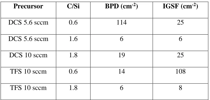
Figure 4.7 Recombination layer (a) thickness and net doping concentration w.r.t C/Si ratio, (b) BPD and IGSF density w.r.t net doping concentration (trend lines shown are guide to the eyes) ...74
Figure 4.8 (a) to (d) NOM images of converted BPDs to TEDs seen on the recombination layer at the corresponding buffer epilayer positions (fig.4.5 (a) to (d)) at different C/Si ratios after KOH etching ...76
Figure 4.9 Net BPD to TED conversion ratio from buffer to recombination layer w.r.t. C/Si ratios...76
Figure 4.10 Schematic of BPD- TED conversion point shift at C/Si =1.0 ...78
Figure 5.1 (a) Bravais lattice of the graphene; (b) σ and π bonds in graphene; (c) graphene π- and π*-band structure ...82
Figure 5.2 (a)The silicon atom has a much larger diameter than the atomic gap in a graphene layer. Si-loss can only occur through defects (Daas et al., 2012). (b) Schematic of defects in graphene, and how they mediate molecular in-diffusion for doping and Si-adatom out-diffusion for growth of EG ...85
Figure 5.3 Mechanism of epitaxial graphene growth using SiF4. In this process, Si is
removed from the surface (steps I–IV). I) Dissociation and Si(l) formation at temperatures >1400°C. II), III) Si is removed efficiently by SiF4 as SiF2 gas. IV) Residual
Figure 5.4 Comparison of as-taken Raman spectra (without substrate subtraction) of on-axis 4H-SiC substrates treated at 1600°C. a) For 1 hour at 10 slm of Ar flow rates without SiF4 and b) for 1 hour at 10slm of Ar with a 10 sccm of SiF4 ...89
Figure 5.5 (a) Temperature dependence of Raman ratio of integrated peak intensities of the D peak to the G peak (ID/IG) indicative of defect density reduction in higher
temperature growth, (b) As temperature increases, the Raman 2D FWHM reduces towards higher carrier mobility for these samples ...90
Figure 5.6 AFM height images (5 x 5 m2) of epitaxial graphene films grown on different offcuts of 4H-SiC substrates ...94
Figure 5.7 AFM phase images (5 x 5 m2) of epitaxial graphene films grown on different offcuts of 4H-SiC substrates ...94
Figure 5.8 XPS C(1s) spectrum of ~14 ML EG showing C(1s) graphene component and Si(2p) SiC bulk component (not obvious because of the thickness > 10 ML) ...96
Figure 5.9 XPS data (Gaussian curve fitted) and thicknesses of EG grown on 4° offcuts for ramp down rates (a) 14℃/min, (b) 28℃/min and (c) 56℃/min ...97
Figure 5.10 FTIR spectra of EG grown on 4° substrates at different ramp down rates ....98
Figure 5.11 Fabrication process flow for EG/SiC vertical schottky diodes ...100
Figure 5.12 Forward I-V characteristics of EG/SiC Schottky diodes grown at different ramp down rates ...101
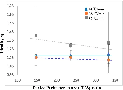
Figure 5.13 Average ideality values for EG/SiC Schottky diodes at different ramp down rates with three different areas (each data point represents an average of 28 devices for the respective areas of the device) ...102
Figure 5.14 Schottky barrier height (Φ𝐵) of EG/SiC Shottky junctions obtained for an average of 28 devices for different P/A of the devices (trend lines shown are guide to the eyes) ...103
Figure 5.15 EG/SiC detector I-V characteristics under dark and 254 nm UV exposure .104
CHAPTER
1
SILICON
CARBIDE
1.1 INTRODUCTION:
Power electronic semiconductor devices are critical components in
next-generation energy-efficient power systems such as hybrid electric vehicles, smart grid
power controls, and high voltage transmission circuitry enabling reduction in system size,
weight, and performance. In the power electronics industry, SiC is setting new standards
in high-performance electrical conductivity, high thermal conductivity, and power
savings. The SiC market in the power electronics industry has widespread application
areas ranging from hybrid vehicles, wind turbines, industrial data centers, medical
imaging, renewable energy, oil and gas, and aerospace. Of these, 4H-SiC is considered
the most viable candidate beyond 3kV due to its technological maturity, owing to the
wide band gap (3.26 eV), high breakdown field (2×10⁶ to 4×10⁶ V/cm), high thermal
conductivity (3 to 5 W/cm/K) and, more importantly, its indirect bandgap. This gives it
much longer minority carrier recombination lifetimes of microseconds vs nanoseconds
for direct bandgap materials such as GaN, making it the only practical wide bandgap for
bipolar devices that require long carrier lifetimes for high current handling.
Despite these promising properties, SiC is not yet a popular material for device
fabrication due to challenges in obtaining high quality single crystal materials. The high
in bulk growth of SiC severely affect the material yield in high scale environments.
Currently SiC wafer technology has shown tremendous improvement for producing high
quality SiC single crystals in bulk as well as epitaxial growths with almost no micropipes
(www.cree.com).
But the method for eliminating BPDs completely from the bulk material is still
under investigation. Identification of the unique and promising properties of SiC have
paved way for rapid increase in research to improve the material quality of SiC single
crystals in bulk as well as epitaxial growths. The low lattice mismatch between SiC and
GaN also makes SiC an excellent substrate for the growth of III-nitrides structures used
in fabrication of blue LEDs and lasers (Gurnett & Adams, 2006; Krüger & Grundmüller,
2013). SiC and SiC based electronic devices fabricated from high quality SiC single
crystals are expected to excel the performance of Si based power devices in the current
market.
1.2 SIC PROPERTIES:
Wide bandgap materials such as SiC, GaN, and diamond have been investigated
to replace the industry workhorse, silicon, due to their superior material properties (Table
1.1). The large bandgap (three times greater than Si) and very low intrinsic carrier
concentration enables device operation at increased temperature (as high as 600 C) and
at high voltages (~10kV). The electric breakdown field of SiC is 5 times higher than Si,
enabling very low specific on-resistance at the same time withstanding high current
densities for SiC devices especially used in high power electronics. The large saturation
conditions. In addition to the wide bandgap electronic properties, the material strength
(chemical stability) of SiC provides a major advantage for devices intended to be used in
harsh environments such as radiation detection, UV detectors in aerospace research,
ignition system and exhaust sensors in automotive industries. Thus, SiC is one of the
promising semiconductor material for fabricating compact high power devices with
increased device performance, decreased size and weight.
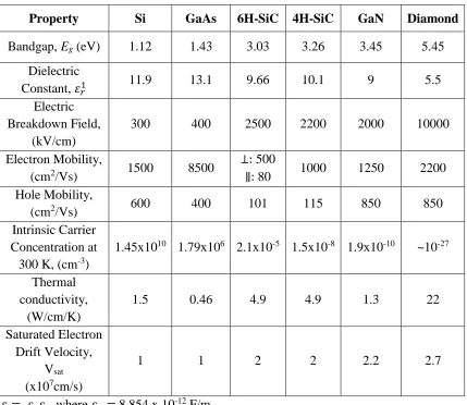
Table 1.1 Properties of various semiconductor materials (Tolbert, Ozpineci, Islam, & Chinthavali, 2003)
Property Si GaAs 6H-SiC 4H-SiC GaN Diamond
Bandgap, Eg (eV) 1.12 1.43 3.03 3.26 3.45 5.45
Dielectric
Constant, 𝜀𝑟1 11.9 13.1 9.66 10.1 9 5.5
Electric Breakdown Field,
(kV/cm)
300 400 2500 2200 2000 10000
Electron Mobility,
(cm2/Vs) 1500 8500
⊥: 500
∥: 80 1000 1250 2200 Hole Mobility,
(cm2/Vs) 600 400 101 115 850 850
Intrinsic Carrier Concentration at
300 K, (cm-3)
1.45x10¹⁰ 1.79x10⁶ 2.1x10⁻⁵ 1.5x10⁻⁸ 1.9x10⁻¹⁰ ~10-27
Thermal conductivity,
(W/cm/K)
1.5 0.46 4.9 4.9 1.3 22
Saturated Electron Drift Velocity,
Vsat
(x107cm/s)
1 1 2 2 2.2 2.7
1𝜀 = 𝜀
SiC crytsal structure and polytypes:
Silicon Carbide is a group IV-IV compound naturally occurring in the rare
mineral Moissanite. Silicon carbide is useful for commercial and industrial applications
due to its hardness, optical properties and thermal conductivity. Efforts to synthesize
silicon carbide in a laboratory began in the late 1800s. Each silicon atom in the crystal is
mostly covalent bonded (89% covalent and 11% ionic) to four carbon atoms and vice
versa in a tetrahedral arrangement (fig.1.1). The strong bonding (4.53 eV) and short bond
length (1.89Å) between Si-C atoms provides SiC it’s very hard material strength. SiC
does not melt but sublimes above 2100℃ at atmospheric pressure (Ellison, 1999).
Figure.1.1 Tetrahedral basic unit of SiC Figure.1.2 ABC sites in hexagonal crystal lattice
In the tetrahedron shown in fig.1.1, it is to be noted that the basal plane consisting
of three silicon atoms and the next plane of silicon atoms are separated by dplane Si−plane Si =
0.252 nm, which is used for calculating the unit cell height of SiC. The plane containing
the carbon atom in the tetrahedral interstitial space is dplane Si−plane C = 0.063 nm from the
basal plane. SiC occurs in many different crystal structures called polytypes. Even though
all SiC polytypes chemically consist of 50% carbon atoms covalently bonded with 50%
tetrahedral bilayer orientation (stacking order and rotation) in a SiC crystal controls the
lattice arrangement and hence its material properties. Two basic configurations arise from
the stacking of successive basic tetrahedral units: either hexagonal (ABAB stacking) or
cubic (ABC stacking) (fig.1.2).
While there are over 200 known polytypes of SiC (Fisher & Barnes, 1990), only a
few are commonly grown in a reproducible form acceptable for use as an electronic
semiconductor. These polytypes are characterized by the stacking sequence of the
bilayers of the SiC structure. SiC polytypes are named based on the number of stacks
(periodicity) before the sequence is repeated and the crystal symmetry. The most
common polytypes of SiC presently being developed for electronics are the cubic
3C-SiC, the hexagonal 4H-SiC and 6H-3C-SiC, and the rhombohedral 15R-SiC (fig.1.3). Change
in the stacking sequence has a profound effect on the electrical properties. The band gap
changes from 3.23 eV for 4H to 2.36 eV for 3C polytype (Levinshtein, Rumyantsev, &
Shur, 2001). 3C-SiC is the only form of SiC with a cubic crystal (zinc blende) lattice
structure and referred to as -SiC. The non-cubic polytypes of SiC are referred to as
-SiC. If the stacking of the bilayer is ABAB ..., then the symmetry is hexagonal (wurtzite)
and referred to as 2H-SiC (fig.1.3). All the other SiC polytypes are a mixture of the
zinc-blende and wurtzite bonding. 4H-SiC consists of an equal number of cubic and hexagonal
bonds with a stacking sequence of ABCB. 6H-SiC is composed of two-third cubic bonds
and one-third hexagonal bonds with a stacking sequences of ABCACB. The overall
symmetry is hexagonal for both polytypes, despite the cubic bonds which are present in
each. Similarly, 15R-SiC is a rhombohedral crystal structure composed of three-fifth
denote Si-C double layers that reside in quasi-hexagonal or quasi-cubic environments
with respect to their immediately neighboring above and below bilayers (Ayalew, 2004).
In the 4H stacking sequence of ABCB, all the A sites are the cubic "k" sites and all the B
and C sites are the hexagonal "h" sites. Similarly, in the 6H stacking sequence of
ABCACB, while all the A sites are the hexagonal "h" sites, there are two kinds of
inequivalent quasi-cubic sites for B and C, denoted "k1" and "k2"sites, respectively
(Ayalew, 2004). To understand the SiC growth and related challenges it is essential to
know its common polytypes in terms of stacking sequences, crystal directions, crystal
planes etc. The important SiC polytypes available as substrate material are 4H and
6H-SiC. These polytypes require four and six Si-C bilayers, respectively, to define the unit
cell repeat distance along the c-axis [0001] direction arranged in a hexagonal close
packed (HCP) lattice.
Figure.1.3 Stacking arrangements seen along [1120] direction of SiC polytypes (Ayalew, 2004)
The close packed structures of these hexagonal polytypes can simply be described
a3, c) shown in figure 1.4. In fig.1.4. the [1100] direction is often referred to as the p or
m-axis and the [1120] direction is referred to as a-axis direction. A crystal will behave
differently from different crystal directions due to variation in the stacking arrangement.
Since the hexagonal polytypes are made up of stacked double layers, several
material properties are different along the c-axis or perpendicular to the c-axis. This is
called anisotropy, and the degree of anisotropy is measured by the quotient of a
parameter value along and perpendicular to the c-axis. Anisotropy of 1 is analogous to
isotropic material. Several of the electrical parameters are anisotropic. As an example, for
6H-SiC, the mobility is different along c-axis and perpendicular to c-axis (Neudeck,
2006). Similarly, the crystal growth is different on different planes for growth rates and
polytype replication (homogeneity) due to the variation in atomic packing density along
different crystal directions.
Figure.1.4 Hexagonal unit cell of SiC showing different crystal planes
As all the SiC polytypes consists of repeated stacking along the c-axis, the 0001
surfaces have either Si or C atoms terminated layer named as Si face and C face,
respectively. The 11% ionic bonding in SiC with Si atoms being positively charged
role in the crystal growth process by influencing the polytype stability, the incorporation
of dopants and impurities, and the crystal surface morphology.
1.3 SiC EPITAXIAL GROWTH METHODS:
The first successful growth of high purity SiC crystal using sublimation growth
was developed by Lely (Lely, 1954). Lely’s initial process used a dense graphite crucible
and a porous graphite thin-walled inner cylinder. The SiC powder is loaded between the
inner and outer cylinder and heated to temperatures of 2550-2600◦C in an argon
atmosphere. Spontaneous nucleation of SiC was observed at the inner surface of the
thin-walled cylinder (fig.1.5).
Figure.1.5 Lely process for SiC bulk growth (Saddow & Agarwal, 2004, p. 6)
The Lely method had several limitations in SiC growth such as the extremely high
growth temperatures above 2000˚C and the necessity to have an acceptable growth rate.
This resulted in some serious disadvantages such as the concentration of defects being
(Wijesundara & Azevedo, 2011). A breakthrough came around 1980 with the
introduction of SiC seed crystal sublimation growth. This method uses a high-quality
seed crystal surface to begin the growth process (Tairov & Tsvetkov, 1978). The seeded
sublimation growth is often referred to as the physical vapor transport method (PVT) or
Modified Lely Method (MLM). The main idea is to sublime SiC powder at high
temperatures (T > 2000 ◦ C) and to re-crystallize the Si- and C-containing gas species at a
slightly cooler single crystal seed (fig.1.6).
Figure.1.6 Schematic of a seeded sublimation (SE) or PVT growth reactor (Chaussende, Wellmann, & Pons, 2007)
PVT is currently used as the standard industrial method for producing high quality
SiC wafers owing to the technological improvements and maturity of the process.
Currently 150 mm (6”) 4H-SiC wafers are commercially produced by standard PVT
method by CREE Inc. To make SiC devices superior in comparison to other standard
semiconductor devices, high quality material with fewer defects is essential. Therefore,
today most SiC electronic devices are fabricated on epitaxial layers grown on bulk SiC
instead of directly making them on the wafers sliced from the bulk SiC crystals.
Homoepitaxial growth of SiC refers to the growth of SiC films of same polytype as that
high structural uniformity, more controllability over the vapor phase composition, growth
rate, doping and good reproducibility than the bulk growth (Wijesundara & Azevedo,
2011). Furthermore, since the precursor gas sources are extremely pure, the impurity
concentration of the deposited material is up to three orders of magnitude lower than in
bulk grown SiC and it is possible to grow n-type and p-type layers with good
homogeneity and reproducibility (Ellison, 1999). The nitrogen background doping level
can be decreased by increasing the C/Si ratio in the vapor phase by a theory called
“site-competition epitaxy” (Larkin, Neudeck, Powell, & Matus, 1994) in which the nitrogen
and carbon atoms compete for the carbon vacancies thereby reducing the nitrogen
concentration in the epilayers and boron and silicon atoms compete for silicon vacancies
thereby forming p-type epilayers. Polytype stability was significantly improved by the
concept of step-controlled epitaxy on off-axis oriented (0001) SiC substrates (T. Kimoto,
Itoh, & Matsunami, 1997) .
Homoepitaxial growth of SiC films can be achieved by various means, each with
its own advantages and disadvantages. Selection of a growth technique is determined by
the application requirements and the technological maturity of the technique.
Homoepitaxial techniques for SiC can be categorized into vapor phase epitaxy (VPE),
liquid phase epitaxy (LPE), and vapor-liquid-solid (VLS) epitaxy (Wijesundara &
Azevedo, 2011). The latter is a novel epitaxial approach which shares the common
fundamentals of VLS nanowire and nanotube growth (Givargizov, 1975; Milewski, Gac,
Petrovic, & Skaggs, 1985).
high temperature CVD (HTCVD). Among these, CVD is the most matured and
researched technique for epitaxial growth of SiC. It is the core technique adapted by the
industry for commercial production of epitaxial SiC wafers.
Chemical Vapor Deposition (CVD) (Wijesundara & Azevedo, 2011): In CVD
growth of SiC, carbon- and silicon-containing gaseous compounds, which are termed as
precursor gases are transported to a heated single-crystalline SiC substrate where the
homoepitaxial growth occurs through a surface-induced chemical reaction. Depending on
the polytype and the reactor configuration (hot wall or cold wall), the growth temperature
can be considerably different, but typically, is above 1200˚C.
Cold Wall reactor: The cold-wall configuration is achieved by using a
double-walled quartz tube with water circulated between the walls. The wafer is placed on an
inductively heated graphite susceptor. To ensure the cold-wall conditions, the sample is
placed on a graphite susceptor (fig.1.7(a)). Cold-wall reactors suffer from shortcomings
related to the thermal uniformity of the reactor because the area above the substrate is not
actively heated which in turn causes poor precursor dissociation efficiency, which
directly translates into the growth rate (Wijesundara & Azevedo, 2011).
Hot-wall reactor: The hot-wall reactor concept was first introduced by Kordina
et al (Janzén et al., 1994). A graphite (thermally and electrically conductive) tube that
runs along the entire length of the reactor is placed inside an air/water cooled quartz tube
and the susceptor is placed inside graphite tube (fig.1.7(b)). Thermally conductive
graphite helps in reducing the heat loss due to radiation and consequently, hotwall
maintain thermal uniformity (Wijesundara & Azevedo, 2011). The advantages of using a
hotwall reactor are: They enjoy better thermal uniformity in both lateral and vertical
directions. In comparison, the temperature gradient in the vertical direction over the
substrate surface can be as large as 220K/mm in a cold-wall reactor and that is nearly ten
times higher than what is achievable in a hot wall reactor (Thomas, Bartsch, Stein,
Schörner, & Stephani, 2004). At the same time the major disadvantage due to the low
thermal gradient in hot-wall reactors is the early decomposition of the growth species
causing undesired deposition on the reactor walls (parasitic deposition) and gas phase
nucleation of reactant species falling on the sample surface producing particle defects
leading to decrease in efficiency of the gaseous precursors during the epitaxial growth.
This is a prevailing problem in hot-wall reactors and the key solution to this issue is to
shift to a more thermally stable Si or C precursor.
Based on the deposition pressure, CVD can be categorized into atmospheric
pressure CVD (APCVD) and low pressure CVD (LPCVD). LPCVD is most commonly
used now- a-days as it offers better control of the growth process in terms of gas phase
nucleation and impurity levels.
Liquid phase epitaxy (LPE): LPE is a method to grow semiconductor crystal
layers from the melt on solid substrates. This happens at temperatures well below the
melting point of the deposited semiconductor. In SiC growth, LPE gained interest
following the reports indicating that micropipes can be filled or closed with this
technique (Filip, Epelbaum, Bickermann, & Winnacker, 2004). The solvent in SiC LPE is
silicon and the carbon source is either graphite container or the SiC added to the melt.
Addition of metals e.g. Sc to the melt is also used to increase the C solubility. The driving
force for the epitaxial growth is provided by applying a temperature gradient across the
structure with a higher temperature at the source than at the substrate (Ellison, 1999).
Since the growth takes place from the liquid phase, LPE technique has the advantage to
provide high growth rates (up to 300 um/h) (Syväjärvi et al., 1999) however the surface
morphology is not as good as achieved by the other epitaxial growth techniques.
Molecular beam epitaxy (MBE) (Wijesundara & Azevedo, 2011): Molecular
beam epitaxy (MBE) is usually applied to grow very thin epitaxial layers. Consequently,
the growth rate is in the order of nanometer per hour and normally the growth
temperature should be quite low. For the controlled growth of SiC hetero-polytypic
structures, consisting of few monolayers each of hexagonal and cubic polytypes, the
growth conditions can be changed from low temperatures (1550 K) and an Si-rich Si/C
ratio (3C-SiC) to higher temperatures (1600 K) and a more C-rich environment (4H-SiC)
1.4 STEP CONTROLLED SiC EPITAXY:
During the crystal growth process by CVD method, the gas molecules (growth
species) in the gas phase approach the sample surface from different directions. Crystal
growth on a c-plane (or basal plane) can take any arbitrary polytype when these gas
molecules approach the surface as it is impossible to know the polytype (stacking
arrangement) from the c-plane. So, growth on a c-plane (0001) is highly unpredictable
since it does not expose any template needed for polytype replication during growth.
Homogeneous crystal is highly essential for the realization of SiC devices.
As first realized by Frank in 1949, dislocations intersecting the surface of the real
crystals provide the source of steps required for continuous growth of a crystal (fig.1.8).
In 1951, Burton et al published the first quantitative model referred as BCF theory
(Burton, Cabrera, & Frank, 1951) providing a comprehensive understanding of the
surface phenomena involved in crystal growth.
Figure.1.8 Crystal growth initiated by a screw dislocation on an ideal on-axis surface (Burton et al., 1951)
In the late 1980s, successful growth of high-quality homoepitaxial 6H-SiC with a
are at a relatively small angle to the basal plane), or off-axis (off-oriented) substrates was
reported (Kong, Glass, & Davis, 1988; Powell et al., 1990) by partially exposing the m-
planes or a-planes in SiC crystal to create a template for polytype imitation by cutting the
original crystal boule at an angle which is called the offcut angle (fig.1.9). The surface
steps existing on the off-oriented substrates serve as a template for replication of the
underlying polytype. This technique of growing epilayers on off-axis substrates is known
as “step-controlled epitaxy” as described by Matsunami and Kimoto (T. Kimoto et al.,
1997).
Figure.1.9 4H-SiC crystal showing offcut plane towards [112̅0] direction
This method was a significant breakthrough in homoepitaxial growth of SiC as it
enabled production of high quality single crystal epilayers with replication of substrate
polytype at reduced growth temperature than the bulk growth. This is beneficial in
reducing contamination from the reactor wall and minimizing unwanted dopant diffusion.
Fig.1.10. schematically illustrates the epitaxial growth process on (a) a well oriented and
(b) an off-oriented 6H-SiC substrate (Tsunenobu Kimoto & Matsunami, 1994). The well
process proceeds through two-dimensional nucleation on the terraces due to high
supersaturation on the surface. The growth process is controlled by surface reactions such
as adsorption and desorption. Therefore, the primary factor that determines the polytype
is the growth temperature. According to ABC notation, the stacking order of 6H-SiC is
ABCACB while 3C-SiC can be either ABCABC or ACBACB. When 3C-SiC grows on a
well-oriented face (due to the absence of steps), two adjacent nucleation sites may also
lead to double positioned twins (Kong, Jiang, Glass, Rozgonyi, & More, 1988) as shown
in Fig.1.10 (a). The off-oriented substrates possess high step density with narrow terrace
width. The smaller terrace width allows the adatoms to reach the step through surface
diffusion and promotes their lattice incorporation at the step edges. The steps contain
dangling bonds which make them highly reactive and in addition to the step edges the
growth process is governed by more reactive sites at the steps (kinks) resulting
replication of the substrate polytype. The kink sites are very important because molecules
that attach there make more bonds to neighboring molecules than the ones that attach to
the terraces or to flat step edges (see fig.1.11). Consequently, they are more likely to
stick. The initial studies on step-controlled epitaxial were performed on 6H-SiC polytype;
however, later studies show its viability to homoepitaxial growth of other polytypes
(a) (b)
Figure.1.10 Schematic representation of the growth mechanism on (a) well-oriented and (b) off-oriented of 6H-SiC [0001] faces (© AIP 1994)
Growth mechanism on a stepped surface:
The remarkable success in step controlled epitaxy led to extensive research to
understand the growth mechanism and the factors affecting step-controlled growth. The
surface of the substrate is in equilibrium with its vapor pressure, Peq, when the flux of
adsorbed atoms from the vapor equals the desorption rate from the surface (Ellison,
1999). In the kinetic theory of gas approximation, the equilibrium flux density of incident
atoms, J is related to the equilibrium vapor pressure, Peq, by:
J (m-2 sec-1) = √ 𝑁𝐴
2𝜋𝑀𝑘𝑇 𝑃𝑒𝑞 (Eq.1.1)
Where M is the molecular weight, k is the Boltzman constant, NA is the Avagadro’s
Figure.1.11 Surface processes involved on a stepped surface with unit step height h and terrace length 𝜆0 (Ellison, 1999)
The various surface processes involved at equilibrium on a stepped surface are
shown in fig.1.11. The adsorbed species diffuse on terraces toward steps. Some of the
adsorbed species can reach steps or kinks and are incorporated into the crystal, and others
re-evaporate to vapor. The driving force of crystal growth is the supersaturation ratio of
the vapor phase 𝛼, which for an incident flux J of vapor species supplied to the crystal
surface can be defined by: 𝛼 = 𝐽
𝐽𝑒𝑞. When 𝛼 > 1 growth is promoted, whereas 𝛼 < 1
results in evaporation. In the BCF theory, the steps are assumed as uniform and perfect
sinks for the incoming species, that is, the capture probability of adsorbed species at steps
is unity, independent of the direction from which adsorbed species approach the steps.
The adsorbed atoms migrate randomly on the terrace before they get incorporated in the
crystal lattice or desorb. The mean distance s for adsorbed species to migrate on a
‘step-free’ surface before desorption is given by:
𝜆𝑠 = √𝐷𝑠𝜏𝑠 = 𝑎 exp (
𝐸𝑑𝑒𝑠−𝐸𝑑𝑖𝑓𝑓
where s is the mean residence time of adsorbed species, and Ds is the surface diffusion
coefficient, a, k, and T are the jump distance (interatomic distance of the impinging
molecule), Boltzmann constant, and absolute temperature respectively. Edes and Ediff are
the activation energies for desorption and surface diffusion. The growth takes place by
the resulting lateral propagation of surface steps. At a supersaturation 𝛼 > 1, the net flux
of growth species reaching the surface is the difference between the adsorption (J) and
desorption (𝑛𝑠
𝜏0 ) fluxes:
Jnet = J –
𝑛𝑠
𝜏0 (Eq.1.3)
The net vertical growth rate R can then be expressed by the velocity of lateral
advancement of the steps, vstep, determined by the adatom diffusion and the step height, h
and is given by the product of the step velocity and tan𝜃 (tan 𝜃= h/ 𝜆0) (Tsunenobu
Kimoto & Matsunami, 1994),
𝑅 = 𝑣𝑠𝑡𝑒𝑝tan 𝜃 = 2ℎ𝜆𝑠
𝑛0𝜆0(𝐽 −
𝑛𝑠0
𝜏𝑠) tanh(
𝜆0
2𝜆𝑠) (Eq.1.4)
where 𝜃 is the substrate off-angle and 𝑛𝑠0is the density of surface adatom sites (C and Si)
at equilibrium conditions. Thus, the growth rate equation above shows that a surface
controlled growth rate presents an exponential temperature dependence due the adatom
diffusion (𝜆𝑠). When the growth is on well oriented surfaces (misorientation from the
basal plane is less than a degree), the growth rate is surface kinetics limited i.e., strongly
dependent on the temperature resulting in high sensitivity to surface temperature which
needs high activation energy and thus leading to growth rate non-uniformity. In the off
sufficient temperature the growth rate becomes mass transport controlled and increases
with increase in the offcut angle (increased density of steps).
Step bunching in stepped surfaces:
The formation of multiple-height steps (step bunching) has been an attractive but
unresolved subject in crystal growth and surface science. During prolonged growth times
step bunching is generally observed on the epilayer surface, because of coalescence of
elementary steps into macrosteps with larger step height (fig.1.12). The surface is quite
similar to the so-called ‘hill-and- valley (or faceted)’ structure, which often appears on
grown surfaces which are off-oriented (Tsunenobu Kimoto, Itoh, Matsunami, & Okano,
1997; Syväjärvi, Yakimova, & Janzén, 2002). The off-oriented surfaces will rearrange
spontaneously to minimize their total surface energies, even if this involves an increase in
surface area.
Figure.1.12 Schematic of a stepped surface showing regular array of steps and step bunching (Degawa, Minoda, Tanishiro, & Yagi, 1999)
The surface free energies of SiC were calculated to be 2220 erg cm-2 for the Si face
the overall surface energy, the Si face which is normally the growth face of SiC epitaxy
forms ‘hill-and-valley’ structures (step bunching) on the off-oriented surfaces.
Impurity incorporation or Site competition in step controlled epitaxy:
The success of silicon carbide (SiC) for high temperature and high power
electronic applications is dependent upon the ability to produce high quality SiC epilayers
of both n-type and p-type in-situ doping with doping profiles ranging from extremely low
doped epilayers for high voltage devices to degenerately doped layers for minimizing
parasitic resistances (Larkin et al., 1994). Larkin et al, 1994, reported for the first time
that the Si/C ratio within the growth reactor has a strong influence on intentional and
unintentional dopant incorporation of the growing 6H, 3C, and 4H SiC (0001) epilayers.
Specifically, the active n-type (nitrogen) carrier concentration was found to be directly
proportional to the Si/C ratio, whereas, the active p-type (aluminum) concentration was
found to be inversely proportional to the Si/C ratio for epilayer growth on the SiC (0001)
basal plane. Dopants in SiC are believed to occupy specific sites, specifically nitrogen
occupies the carbon site while aluminum occupies the silicon site of the SiC lattice
(Choyke, 1990; Davis & Glass, 1991). The relative increase in carbon concentration in
the precursor gas species “outcompetes” the nitrogen for the C-sites of the growing SiC
lattice. The analogous situation exists for an increased Si/C ratio, in which the relative
increase in silicon concentration “outcompetes” the Al for the Si sites of the growing SiC
lattice. This model is referred as “site-competition” epitaxy and is used to rationalize the
experimental results of active dopant dependence on the Si/C ratio.
Site-competition epitaxy was also successfully used to obtain very abrupt changes
of the dopant profile is limited by the purging of the dopant-source from the growth
reactor. One advantage of epilayer growth using site-competition epitaxy is that more
abrupt dopant profiles can be obtained by excluding the remaining unwanted dopant by
changing the Si/C ratio along with the dopant-source gas (Larkin et al., 1994).
Conversely, very abrupt, enhanced dopant incorporation can be accomplished for
production of highly degenerately doped epilayers. One highly useful example of this is
the ability to form very thin degenerately doped p-type and n-type contact layers by
stopping the source-flow of Si or C, respectively, during the last minutes of epilayer
growth. Subsequently deposited metal contacts are “ohmic as deposited” for a wide
variety of metals on both p-type and n-type epilayers (Larkin et al., 1994).
1.5 STRUCTURAL DEFECTS IN SIC:
The structural defects nucleated in SiC epilayers as well as in the substrates attract
interest because some of them have been demonstrated to be detrimental to device
performance. The main dislocations that are discussed in SiC epitaxy are the micropipes
(MP), threading screw dislocations (TSD), threading edge dislocations (TED), the basal
plane dislocations (BPD) and stacking faults (SF) (N. Zhang, 2011). These common
defects are shown after KOH etching in fig.1.13. Circular, or oval shapes are indicative of
Figure.1.13 Optical microscopy image of SiC epilayer surface showing defects and their effects on the device performance (T. A. Rana, 2013)
Koga et al. in 1992 reported for the first time that a p-n junction presented a very
low breakdown voltage when a micropipe was present (Koga, Fujikawa, Ueda, &
Yamaguchi, 1992). Elementary screw dislocations (TSDs), although not as detrimental as
micropipes, could adversely affect the breakdown voltage of SiC devices and deteriorate
the performance and reliability of SiC power devices (Wahab et al., 2000). The basal
plane dislocations and stacking faults are additional defects that were found to degrade
the SiC device performance (Agarwal, Fatima, Haney, & Ryu, 2007; Sumakeris et al.,
2006).
Screw dislocations (SDs) have both burgers vector and line direction along
c-axis. The screw dislocations observed in SiC are divided as closed-core screw
dislocations (threading screw dislocations, TSDs) and hollow-core screw dislocations
(micropipes, MPs). In hexagonal SiC (4H and 6H) screw dislocations with Burgers
vectors of magnitude two multiples of the c-lattice parameter or less are close-core SDs
due to the large energy needed for screw dislocation formation (Ohtani, Katsuno,
Fujimoto, Aigo, & Yashiro, 2001).
Micropipe (MP) is the defect that has been discussed the most in SiC. The first
topographic observation of the presence of MPs in SiC was done by Dudley et al.(Huang
et al., 1999). MP is a pure screw dislocation with giant Burgers vector along the c
direction. The critical Burgers vectors for a hollow core screw dislocation are 2c and 3c
for 6H and 4H SiC, respectively (Heindl et al., 1998). Micropipe is the most detrimental
defect for high power and high voltage devices because they increase the leakage current
and reduce the breakdown voltage drastically (N. Zhang, 2011). Inheritance of MPs from
the seed is commonly seen in growth of SiC. Also, they may come from the relaxation of
stresses from handling damage on the seed surface. Another possible reason to nucleate
MPs is the relaxation of stresses arising from the incorporation of inclusions of solvent or
impurity which can occur on the seed surface. Filip et al. (Filip et al., 2004) reported the
closure of 80% of the MPs with the diameter less than 5 µm using LPE process. Owing to
the tremendous maturity in SiC bulk growth and wafer processing technology, at present
the MPs density has been reduced to zero for a 3” wafer (www.cree.com).
Threading edge dislocations (TEDs) are pure edge type dislocations with
Burgers vectors (1/3<1120 >) perpendicular to their line directions (along c-axis).
Threading edge dislocation is introduced by extra half (1100) habit plane. Ha et al
reported that the TEDs are mostly inherited from the substrate or converted from bent
BPDs due to image force (Ha, Mieszkowski, Skowronski, & Rowland, 2002). Ha et al.
of TEDs has been reported in SiC devices except for a minor influence in reducing the
minority carrier diffusion lengths (S. Maximenko et al., 2010).
Basal plane dislocations (BPDs) are the defects that lie in the basal plane
(c-plane) of the crystal. The basal plane [0001] is the primary slip plane for 4H and 6H due
to its largest inter-plane distance. These BPDs are screw or mixed (edge and screw) type
depending on the angle between line direction and Burgers vector 1/3<1120 >. BPDs are
formed mostly during the relaxation stress caused by temperature gradients introduced
during cooling down from growth temperature to room temperature (Gao & Kakimoto,
2014).
Both screw and threading edge dislocations propagate perfectly to the epilayer
from substrate, though basal plane dislocation mostly converts into threading edge
dislocation (Ha et al., 2002; Ohno et al., 2004). Lower elastic energy of threading edge
dislocation per unit length along the growth thickness is preferable to form during the
growth than forming the basal plane dislocation of higher elastic energy (Ha et al.,
2002).That is why it is assumed that most of the BPDs convert in to TED during epitaxial
growth. The method of converting all the BPDs in the epilayer into TEDs is of paramount
interest in the field of SiC epitaxy.
Stacking faults (SFs) are planar defects and they mostly exist in the primary slip
plane, which, for SiC, is [0001]. They are formed due to the misalignment in the stacking
order deviating from that of the parent polytype (fig.1.14). Extra energy is needed to
generate the SF and this is called the SF energy. It differs greatly for different polytypes.
SF namely, intrinsic SF (caused due to missing (vacancy agglomeration) of lattice atoms)
and extrinsic SF (formed due to the insertion of extra interstitial layer of lattice atoms).
Hong et al (Hong, Samant, & Pirouz, 2000) reported the stacking fault energy of 4H-SiC
is 14.7±2.5mJ/m2 and that of 6H-SiC is 2.9±0.6mJ/m2. When forward voltage is loaded,
basal plane dislocations with Burgers vector 1/3<1120 > were observed to dissociate into
two Shockley partial dislocations of Burgers vectors 1/3< 10 1 0 > and 1/3< 01 1 0 >. The
Burgers vector is conserved by reaction 1/3<1120> = 1/3<1010>+1/3<0110> with a
ribbon of stacking fault between the two Shockley partials (N. Zhang, 2011).
The existed stacking faults were also found to expand through the motion of
Si-cored partials under forward bias. These Formation and expansion of basal plane stacking
faults bounded by partial dislocations were interpreted as the reason for the degradation
of forward voltage (S. I. Maximenko, Pirouz, & Sudarshan, 2005)
1.6 STATE OF THE ART SiC WAFER AND DEVICE TECHNOLOGY:
Due to the persistent research in improving the quality of SiC bulk growth and
processing technology, SiC wafers currently exhibit tremendous increase in quality. At
present, a 4H-SiC 3” highly conducting wafer is obtained for ~$550 (CREE Inc., 2016).
SiC 3” wafers with zero micropipe density and a BPD density of 500 to 800 cm-2 [II-VI
epiworks, Dow Corning and CREE Inc]. SiC power MOSFETs, Schottky diodes and
IGBTs are commercially available with a temperature withstanding capability of 225℃
[ROHM semiconductor]. SiC sensor market has also shown an increase in demand for its
applications in harsh environments such as radiation detectors, UV detectors, exhaust gas
sensing in automobiles and industries. Epitaxial Graphene on Silicon Carbide is a newly
maturing technology owing to the versatile properties of graphene especially in the solar
energy, fuel cells and other sensory applications. With the raising popularity and demand
for SiC devices, the necessity to improve the quality of SiC epitaxy is the need of the
CHAPTER 2
HOMOEPITAXIAL GROWTH OF 4H-SiC USING HALOGENATED
PRECURSORS
2.1 INTRODUCTION:
Homoepitaxial growth of SiC is one of the key processes in the fabrication of SiC
devices. As mentioned in the previous chapter, though various methods are attempted in
SiC epitaxial growth, chemical vapor deposition (CVD) is still the leading and the most
attractive technique to grow thick and high quality epitaxial SiC layers for high power
devices. One of the significant challenges in obtaining high quality thick SiC epitaxial
films is to restrict/eliminate the Si gas-phase nucleation or aerosol formation during
growth which is caused by the early decomposition of the growth species before reaching
the surface of the substrate. The generated aerosol particles adversely influence growth
by reducing the growth rate due to precursor losses, and affect crystal quality (Segal et
al., 2000), since the Si droplets are carried to the crystal growth surface. Moreover, liquid
aerosol particles adhere to the various reactor parts (parasitic deposition), and contribute
to their severe degradation during epitaxial growth. These parasitic depositions are
generally loosely bound, and can be carried to the growth surface during growth as
particulates, resulting in degradation of crystal quality by introducing defects in the
The conventional SiC-CVD process uses silane (SiH4) as the Si-precursor, light
hydrocarbons e.g. propane (C3H8) or ethylene (C2H4) as the C-precursor, and hydrogen as
the carrier gas. Using Silane precursor, the gas decomposition starts early in the gas
delivery system and leads to severe parasitic deposition in the reactor system and
degradation of epilayer morphology due to particulates deposition on the growth surface
(T Rana et al., 2012).
In recent years, chloride precursors such as CH3Cl3Si (Methyltrichlorosilane,
MTS), SiH2Cl2 (Dichlorosilane, DCS), SiCl4 (Tetrachlorosilane, TCS) and/or HCl
addition are induced to achieve high growth rate and to reduce Si-droplet formation in 4H
and 6H SiC-CVD process (Chowdhury, Chandrasekhar, Klein, Caldwell, & Sudarshan,
2011; Dhanaraj et al., 2006; La Via et al., 2006; Lu, Cheng, Zhao, Zhang, & Xu, 2009).
Recently, tetrafluorosilane (TFS, SiF4), a fluorine based gas having the strongest
Si-halogen bond (Si-F bond energy 565kJ/mol vs. Si-Cl bonding energy 381kJ/mol)
(Kolditz, 1967), has been introduced as a novel Si-precursor in SiC epitaxial growth
(Sudarshan, Rana, Song, & Chandrashekhar, 2013). As a thermodynamically stable
compound, TFS breaks to elemental compounds only at a very high temperature above
2000˚C (fig.2.3) (Collins, 2000). Interestingly, it reacts with C-containing species at a
temperature less than 2000˚C to facilitate the epi-growth of SiC. This deposition possible
with presence of a hydrocarbon gas indicates that the hydrocarbons plays an important
role in SiC growth by SiF4. This temperature stability of TFS makes it a potential
Si-precursor in SiC epitaxial growth by inhibiting parasitic deposition by 80% and
eliminating Si droplet formation during SiC epitaxial growth (T Rana, Chandrashekhar,
2.2 COMPARATIVE STUDY BETWEEN DCS AND TFS PRECURSORS:
A systematic study of parasitic deposition and its influence on the precursor
efficiency for various precursors in the reactor is essential to improve the epitaxial
growth. In this chapter, we report the results and discussion of a comparative study on 4°
offcut SiC substrates between the halogenated Si precursors SiH2Cl2 (DCS) and SiF4
(TFS) used in the author’s group for SiC homoepitaxy.
EXPERIMENTAL SETUP:
Epitaxial growth of SiC is carried out using an inverted chimney type vertical
hot-wall CVD reactor (fig.2.1). This arrangement consists of a hot-hot-wall, a gas injector and a
substrate holding susceptor. TFS / DCS and propane are used as precursor gases. DCS or
TFS was used as the Si-precursor with standard flow rates at 5.6 sccm and 10 sccm,
respectively. Propane was used as the C precursor. Hydrogen was the carrier gas with a
flow rate of 10 slm. Growths were performed for different C/Si ratios (from 0.3 to 2)
keeping constant Si and varying the C flow rates. The growth temperature and pressure
were 1600°C and 300 torr. The growth recipe is shown in fig.2.2. Commercially available
4H-SiC wafers (4 off cut towards [11-20], optically polished) cut into 8 mm × 8 mm
pieces were used as the substrate for all the growth experiments in this study. The gas
delivery system in the CVD reactor contains an injector tube and a funnel as shown in
fig. 2.3 (a&b). The injector tube is axially split into two half parts (fig. 2.3a). This split
tube can be assembled to form a complete tube before growth and can be observed after
the growth by separating them. The parasitic deposition generated during the growth run
Figure.2.1 Schematic diagram of the CVD furnace used for SiC growth (T. A. Rana, 2013)
The epilayer thickness was measured using the fourier transform infrared reflectance
(FTIR) spectroscopy and mercury probe C-V analysis technique was used for measuring
the net unintentional doping concentration of the epilayers. The epilayer surface
morphology was studied using an atomic force microscope (AFM) and Nomarski optical
microscope (NOM), KOH etching was performed to determine the defect density in the
Figure.2.2 SiC- CVD epitaxial growth recipe using TFS/DCS Si precursor
(a) (b)
Figure.2.3 a) Axially split injector tube and b) Injector funnel before growth
2.3 PARASITIC DEPOSITION AND GROWTH RATE COMPARISON:
As explained previously, parasitic deposition is one of the major reasons that
limits epilayer quality and causes high fabrication cost (T Rana et al., 2012). It occurs
because of the decomposition/reaction of the precursors on the surface of the reactor wall,
before reaching the substrate. The parasitic deposition is severe for high growth rate
and temperature distribution obtained by simulation using Virtual Reactor. Fig. 2.5 shows
the split injector tube and bottom view of the injector funnel (cap) before and after
growths using DCS and TFS for the same C/Si ratio = 1.8 and Si flow rate (10 sccm).
The parasitic deposition could be found as yellowish depositions on the walls.
Figure.2.4. CVD furnace geometry and temperature distribution simulated using Virtual Reactor (T Rana et al., 2012)
For DCS-growth, the parasitic deposition starts at ˜900°C, reaches the maximum
at ˜1250°C on the injector tube (Fig. 2.5b), and then reduces on the injector cap (Fig.
2.5e), whereas for TFS-growth, the parasitic deposition occurs at ˜1400°C mostly on the
injector cap (Fig. 2.5f). By weighing the injector tube and cap before and after epigrowth,
the overall parasitic deposition in TFS-growth is much less (˜80%) than that in
Figure.2.5 Deposition on injector tube (split) and Injector cap (funnel) (bottom view) for 1 hour growth with 10 sccm DCS or TFS. (a) and (d):before growth; (b)
and (e): after DCS-growth; (c) and (f): after TFS-growth (Balachandran, Song, Sudarshan, Shetu, & Chandrashekhar, 2015)
Ideally TFS should not exhibit parasitic deposition at a temperature below 2000˚C
due to its high temperature stability (fig.2.6). Experimentally, deposition of 3C-SiC is
observed (confirmed by Raman spectroscopy) in TFS growth on the injector funnel
where the temperature is ~1400˚C. It has been shown that the decomposition and reaction
of TFS in the gas-phase is mediated by C-containing species. There are several potential
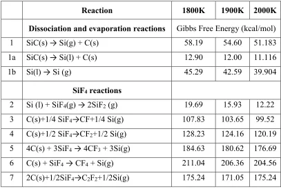
reaction pathways that have been proposed (T Rana et al., 2013) as shown by Table 2.1.
These reactions are all possible below the 2000 ˚C decomposition temperature for TFS.
But it is evident that the presence of hydrocarbons makes TFS decompose (dissociate) at
a temperature below 2000˚C resulting in parasitic deposition on the injector cap portion
(T Rana et al., 2013). Surface reaction kinetics also play an important role on TFS
decomposition in the presence of C-containing species. This also suggests that the
epi-growth of SiC using TFS is carbon mediated. Optimization of the reactor geometry (e.g.,
increasing the temperature gradient above the susceptor) can further reduce the parasitic
in the SiC epilayer properties such as growth rate, unintentional doping, surface
morphology and defects is necessary for identifying the superiority of the precursors to
obtain high quality SiC epilayers, which is one of the main objectives of the research
presented in this chapter.
Figure.2.6 Temperature versus Gibbs free energy of thermal decomposition reactions of SiH4, SiH2Cl2 and SiF4 (Sudarshan et al., 2013)
2.4 GROWTH RATE VS. C/Si RATIO:
The growth rates at various C/Si ratios are shown in Fig.2.7. It can be seen that
for DCS, the growth rate increases with C/Si ratio when C/Si<1 and saturates for C/Si >1.
This indicates that the growth is C supply limited for C/Si<1 and Si-supply limited for
C/Si>1. However, for TFS-growth, the growth rate continually increases with C/Si ratio
up to C/Si=2. This suggests a strong C supply dependent growth mechanism for TFS
growth. It should be noted that for TFS-growth, even at high Si flow rate (10 sccm), the
growth at 10 sccm (C/Si ratio =1.8, growth rate 21.5 um/hr) has more particle defects (~
5/cm2) than DCS at 5.6 sccm (no particles). This is due to the increase in parasitic
deposition and Si droplet formation on the injector with increase in DCS flow rate.
Figure.2.7 Growth rate vs. C/Si ratio for for DCS and TFS-growths at different flow rates (Trend lines shown are guide to eyes) (Balachandran et al., 2015).
In step-controlled epitaxy, at typical temperatures, the growth is mainly limited by
the diffusion of growth species into the boundary layer (the region near the surface of the
substrate where the gas flow velocity, concentration of growth vapor species and
temperature changes from the bulk gas flow region) (Tsunenobu Kimoto, Nishino, Yoo,
& Matsunami, 1993). Increased growth rate at increased temperatures is shown to be due
to the increased diffusivity of the gas molecules in the boundary layer at elevated
temperatures. The non-saturating growth rates seen in TFS at high flow rate (10 sccm) is
attributed to the mass transport limited growth with increase in precursor efficiency by
Table.2.1 Free formation energy (kcal/mol) for various SiC etching reactions calculated from JANAF thermochemical data (T Rana et al., 2013)
2.5 UNINTENTIONAL NET DOPING CONTROL VS. C/Si RATIO:
Grown SiC epilayers were examined using mercury-probe C-V technique to
determine the net doping concentrations. Fig. 2.8 shows the unintentional doping
concentration at various C/Si ratios for both DCS and TFS. Both the curves show doping
dependence behavior agreeing with the “site competition” theory (Larkin et al., 1994).
TFS-growth produces doping concentration by an order of magnitude lower than for
DCS-growth at the same C/Si ratio. It should be noted that in TFS growth the precursor
is of narrow range (C/Si ratio 1.6 to 1.8) compared to TFS (C/Si ratio 1.5 to 2)
(Balachandran et al., 2015).
(a) (b)
(c)
Figure.2.8. (a) Net doping concentration vs. C/Si ratio for (a) TFS (at 10 sccm), (b)TFS (at 5 sccm) and (c) DCS (at 5.6 sccm) growths
The weak site competition in TFS growth is attributed to the strong Si-F bond and
affinity. The high bond strength between F and Si increases the surface resident time of
Si-F molecules impinging the growth surface. This increases the probability of elemental
F to get incorporated in the crystal and C atoms being less mobile also stay on the
![Figure. 4.1 BPD with dislocation line parallel to the [11-20] off-cut direction (Z. Zhang & T](https://thumb-us.123doks.com/thumbv2/123dok_us/8373949.1384207/78.612.221.406.157.268/figure-bpd-dislocation-line-parallel-cut-direction-zhang.webp)