Analysis, Design and Implementation of
Snubberless Bidirectional Current Fed Full
Bridge Voltage Doubler
Vinay.K.V1, Raju Yanamshetti2, Ravindra .Y.N3
PG Student [Power Electronics], Dept. of EEE, PDA College of Engineering, Kalaburgi, Karnataka, India1 Professor, Dept. of EEE, PDA College of Engineering, Kalaburgi, Karnataka, India2
Assistant Professor, Dept. of Electronics, SMT. VG College for women, Kalaburgi, Karnataka, India3
ABSTRACT: this paper describes the novel soft switching bidirectional snubberless current fed full bridge voltage doubler. A novel secondary modulation technique is used to clamp the voltage across the primary side switches naturally with zero current commutation (ZCC). It eliminates the necessity for active clamping or passive snubber to absorb the switch turn off voltage. A major challenge in current fed converters, zero current switching (ZCS) of primary side devices and zero voltage switching (ZVS) of secondary side devices are achieved, which significantly reduce switching losses. Primary device voltage is clamped at low voltage, which enables the use of low voltage devices with low on state resistance. Soft switching and voltage clamping is inherent and load independent.
KEYWORDS: snubberless, Bidirectional, zero current commutation (ZCC), zero current switching (ZCS), zero voltage switching (ZVS).
I.INTRODUCTION
Bidirectional dc/dc converter isolated with high frequency transformer has been widely used in motor drives in electrical vehicles (EVs), energy storage systems (ESS), dc/dc converting stage of solid state transformers (SSTs), and hybrid renewable energy generation with ESS due to its merits of low cost and high power density[1-5]. The proposed design DC-DC converter has the following features: number of active devices are low compared to the converters usually applied to reduce switching losses, DC-DC converter is essential equipment in the system of dc load which has step up and step down voltage. A DC-DC converter is required electrical couple to the dc load.
In the full bridge DC-AC-DC converter which allows energy transfer between the source and the load. The performance of the converter will be analyzed by comparing various modulation techniques like phase shift, triangular and trapezoidal methods. A high frequency transformer is used for isolation in DC-DC full bridge voltage doubler. Various modulation strategies have been discussed for the dual active bridge DC-DC converter [6]. The performance parameters have been analyzed in terms of output voltage ripple and switching losses. Simulation studies have been carried out using MATLAB & SIMULINK to verify the results.
Compared to voltage fed converters, current fed converters have lower input current ripple, lower HF transformer turns ratio, negligible diode ringing [8], and easier current control ability. Therefore current fed converters are meritorious for low voltage and high current application. The major limitations of current fed converters are hard switching and snubber requirements to absorb the switch turn off voltage spike.
A dual half bridge bidirectional DC-DC converter is proposed to minimize the number of switching devices. This converter topology requires four split capacitors to handle full load current and occupy a considerable volume of the converter. It may need an additional control to avoid the possibility of voltage imbalance across the capacitors. Also this topology is not modular in nature and so not easily scalable for higher power. Peak current through the primary switches are ˃2x the input current and top and bottom switches share unequal currents. In this paper, a novel secondary
II.
BLOCK DIAGRAM AND DESCRIPTIONFig.1 Block diagram
In this paper, a secondary modulation based soft switching bidirectional snubberless current fed full bridge voltage doubler is proposed as shown in Fig.2
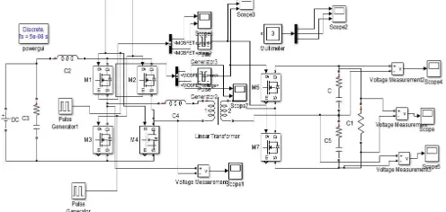
Fig.2 snubberless bidirectional full bridge voltage doubler
Voltage doubler or half bridge is selected to reduce number of switches; the transformer turns ratio. The proposed converter offers the following merits:
1) Switching losses are reduced due to ZCS of primary switches and ZVS of secondary switches. It permits high switching frequency operation to realize a compact and high power density system.
2) Voltage across primary devices is independent of duty cycle with varying input voltage and output power and naturally clamped. It avoids the need of passive snubber or active clamping circuit making it snubberless and enables the use of semiconductor devices of low voltage rating having low on state resistance. Therefore the conduction loss is significantly reduced and high frequency can be achieved.
III.SWITCHING OPERATION
In this section, steady state operation and analysis with zero current commutation (ZCC) natural voltage clamping (NVC) concept has been explained. Before turning off of a diagonal switch pair (S1-S4 or S2-S3) at primary side, the
other pair of primary side switches turned on. The reflected output voltage V0/2n appears across the transformer
primary. It diverts the current from one switch pair to other pair through transformer causing current through just triggered switch pair to raise and the current through conducting switch pair to fall to zero naturally resulting in ZCC. Later the body diodes across switch pair start conducting and their gating signals are removed leading to ZCS turnoff of devices. Then the device voltage raises and clamped at reflected output voltage. For the simplicity the study of operation and analysis, the following assumptions are made: A) boost inductor L is large enough to keep constant current. B) All active and passive components are assumed ideal. C) Series inductor Llk includes the leakage inductance
of HF transformer. With appropriate design of the HF transformer, external series inductor could be avoided. D) Magnetizing inductance is infinitely large.
Steady state operating waveforms are shown in Fig.3. the primary switch pairs S1-S4 and S2-S3 are operated with
identical gating signals phase shifted with each other by 1800. The duty cycle is kept higher than 50%. The operation
Interval 1 (Fig.4a; t0˂ t ˂ t1 ): In this interval, primary side H-bridge switches S2 and S3 anti-parallel body diode D6
of secondary side switches are conducting. The current through series inductor Llk is negative and constant. Power is
transfer to the load through HF transformer.
Interval 2 (Fig.4b; t1 ˂ t ˂ t2 ): At t = t1, primary switches S1 and S4 are turned on. The corresponding snubber
capacitors C1 and C4 discharge fastly in a very short period.
Interval 3 (Fig.4c; t2˂ t ˂ t3): Now all four primary switches are conducting. Reflected output voltage V0/2n appears
across series inductor Llk and diverts the current through switches S2 and S3 into switches S1 and S4. Therefore, primary
current starts increasing linearly. It causes currents through previously conducting devices S2 and S3 to reduce linearly
while switches S1 and S4 start conducting with zero current which helps reducing associated turn-on loss. Since the
anti-parallel body diode D6 is conducting. S6 can be gated on for ZVS turn on. At the end of this interval, D6
commutates naturally. Primary current of transformer reaches zero and ready to change polarity.
Fig.3 operating waveforms
Interval 4 (Fig.4d; t3˂ t ˂ t4): in this interval, secondary side swich S6 is turned on with ZVS. Currents through all the
switching devices continue increasing or decreasing with the same slope as interval 3. At the end of this interval, the primary devices S2 and S3 commutate naturally and their respective currents reach zero obtaining ZCS. The full current,
Interval 5 (Fig.4e; t4˂ t ˂ t5): In this interval, the primary or series inductor current increases further with the same
slope and anti-parallel body diodes D2 and D3 are start conducting causing extended zero voltage to appear across the
outgoing or commutated switches S2 and S3 to ensure ZCS turn off. Now the secondary device S6 is turned off.
At the end of this interval, currents through transformer, switch S1 and switch S4 reach their peak value. This interval
should be short to limit the peak current through the components reducing the current stress and kVA ratings.
Interval 6 (Fig.4f; t5 ˂ t ˂ t6): During this interval, switches S2, S3 and S6 are turned off. Anti-parallel body diode of
switch S5 takes over the current immediately. Therefore, the voltage across the transformer primary reverses polarity
and the current through it starts decreasing. The currents through the switches S1 and S4 and body diodes D2 and D3
also start decreasing.
At the end of this interval, currents through D2 and D3 reduce to zero and diodes are naturally commutated.
Interval 7 (Fig.4g; t6˂ t ˂ t7): In this interval, snubber capacitors C2 and C3 charge to V0/2n. switches S2 and S3 gain
forward blocking mode.
Interval 8 (Fig.4h; t7˂ t ˂ t8): In this interval, currents through S1 and S4, transformer are constant at input current Iin
and current through anti-parallel body diode of the secondary switch D5 is Iin/n.
For the rest of HF cycle, the intervals are repeated in the same manner with other symmetrical devices conducting to complete the full HF cycle.
IV.DESIGN PROCEDURE
In this section, design procedure is illustrated by a design example considering the following specifications:
Po=250W, Vin=12V, Vo=150 ~ 300V, fs=100kHz. The design equations are presented to calculate the components rating.
(1) Average input current is Iin=Po/(ηVin).Assuming an ideal efficiency η of 95%, Iin=21.9 (2) Maximum voltage across the primary switches is
, =2∙ (1)
(3) Input and output voltages are related as
= ∙
1− (2)
Where d is the duty cycle of primary switching devices.. Equation (2) is derived by assuming body diode conducts for quite short time just to ensure ZCS of primary switches(interval 6) without significantly increasing the peak current. However, at light load, the diode conduction time is relatively large and (2) not valid any more. Due to the existence of longer body diode conduction period, the output voltage is boosted to higher value than that of nominal boost converter. For such cases, (2) is modified into following
= ∙
(1− − ′) (3)
Where d’ given by,
= −0.5−4∙ ∙ ∙ _ ∙
2∙ (4)
(4) Series inductance Llk is calculated using
= ∙( −0.5)
4∙ ∙ ∙ (5)
(5) The output power can be derived as
=4 ∙ − ∙ ∙(3−4 )
16∙ ∙ ∙ (6)
Turns ratio of HF transformer is selected based on conduction losses, which mainly consist of the conduction losses in the primary switches because they carry higher currents. Increasing the turns ratio may reduce the maximum voltage across the primary switches allowing low voltage switches with low on state resistance. but, higher turns ratio yields high switch rms current. Voltage regulation over varying input voltage is another concern. An optimum turns ratio n=5 and duty cycle d=0.8 are selected to achieve low overall conduction losses. Output voltage can be regulated from 150V to 300V by varying the duty cycle. Leakage inductance of Llk=2.05µH is obtained from (5) for the given values.
(6) Value of boost inductor is given by
= . ( −0.5)
∆ ∙ (7)
Where, Iin is the boost inductor ripple current. For I = 1A,
(7) the current and voltage stress of major components are given in Table I. Table I Current and Voltage stress of major components
(8) VA rating of each HF transformer is given by
= ∙
2
2∙(5−4 )∙(1− )
3 (8)
V.EXPERIMENTAL RESULTS
A) SIMULATION RESULTS
The proposed converter has been simulated using MATLAB & SIMULINK 2013b. Simulation results are illustrated in Fig.6, which coincides closely with theoretical operating waveforms in Fig.3
INPUT VOLTAGE: 12V DC
OUTPUT VOLTAGE: Fig.6(a) clearly shows the output voltage across resistor which is the total voltage of both output capacitors.
(a)
GATING SIGNALS TO THE MOSFETS: Fig.6(b) shows the gating signals generated to trigger the primary and secondary switches(MOSFET’s).
(b) MOSFET VOLTAGE AND CURRENT:
(c)
SWITCHING VOLTAGE AND CURRENT: Fig.6(d) shows the switching current and voltage, which indicates the ZCC of switches.
(d)
B) HARDWARE RESULTS
The hardware implementation of proposed converter prototype is shown in Fig.7. in proposed converter all subsystems such as transformer, MOSFET switch, capacitor and controller parts are implemented.
Fig.7. converter hardware Constant load: 470 ohms. Duty cycle (%) Voltage (V)
60 70
70 86
80 110
Constant dutycycle:70% Resistance (ohms) Voltage (V)
100 54
470 86
570 92
VI.CONCLUSION
A novel soft switching bidirectional current fed full bridge voltage doubler is proposed. Steady state operation, analysis and design are illustrated. Simulation results clearly demonstrate that the proposed converter maintains ZCS of primary devices and ZVS of secondary devices. Proposed novel modulation technique clamps the voltage across the primary side switches naturally with ZCC and therefore eliminates the necessity for active clamp or passive snubbers required to absorb device turn off voltage spike. Soft switching and voltage clamping is inherent and is maintained independent of load. Usage of low voltage devices leads to low conduction losses in primary switching devices, which is significant due to higher currents on primary side. The converter is suitable for higher boost ratio and high current applications, i.e., interfacing low voltage to higher voltage DC bus with higher current such as fuel cell vehicles.
REFERENCES
[1] Du, Yu, Srdjan Lukic, Boris Jacobson and Alex Haung. “Review of high power isolated bi-directional DC-DC converters for PHEV/EV DC charging infrastructure.”in Proc .IEEE Energy conversion congress and exposition, 2011, pp.553-560.
[2] T.F. Wu, W.C. Chen, J.G.Yang. “isolated bidirectional full bridge dc-dc converter with flyback snubber,” IEEE Trans. Power Electron, vol.25, no.7, 2010, pp.1915-1922.
[3] H. Qin and J.W.Kimball. ‘‘Ac-ac dual active bridge converter for solid state transformer,” in Proc. IEEE Energy conversion congress exposition,
sep 2009, pp.3039-3044.
[4] A.K Rathore and Prasanna U R. “Analysis, design and experimental results of novel snubberless bidirectional naturally clamped ZCS/ZVS current fed half bridge dc/dc converter for fuel cell vehicles,” IEEE Trans. on Ind. Electron, vol.60, 2013, pp.4482-4491.
[5] Kim, Myoungho, Anno yoo and Seung ki sul. “A new universal isolated converter for grid connection,” IEEE Tran.on Ind Applications,vol 48, no.2, 2012: pp.685-696.
[6] F.Krismer, S.Round and J.W.Kolar, “performance optimization of a high current dual active bridge with a wide operating voltage range,” in
Proc.37th IEEE PESC, jun 2006, pp.1-7.
[8] A.K. Rathore and Prasanna U.R. “comparison of soft switching voltage fed and current fed bidirectional isolated DC-DC converter for fuel cell vehicles,” in Proc. IEEE ISIE, may 2012, pp.252-257.
[9] Y.Miur, M. Kaga, and Y. Horita, “Bidirectional isolated dual full bridge dc-dc converter with active clamp for EDLC,” in Proc.IEEE ECCE,
2010, pp.1036-1143.Y.
[10] F.Z. Peng, H. Li, and S.Lawler, “A new ZVS bidirectional dc-dc converter for fuel cell and battery application,” in IEEE Trans. Power Electron,