Design Methodology for Operational
Trans-Conductance Amplifier by using Multi
Objective Optimization Techniques
Abhinav Boddupalli1B.Tech, IVth year , EEE, NIT Bhopal, Madhya Pradesh, India1
ABSTRACT: Operational Trans-conductance Amplifier (OTA) also known as the voltage to current converter generates output current from a differential input voltage and hence it is a Voltage Controlled Current Source (VCCS). It’s ideal characteristics are linear in nature and is similar to Op-Amp (Operational Amplifier) in that there exists high impedance differential input stage and also that it can be used with negative feedback but it is not as much use as Op-Amp in standard op-amp functions due to its output which is current. Often most of these require good linearity over a significant input range along in addition to low noise and current consumption. The deviation from ideal nature may occur either due to transistor mismatch or transistor deviation from perfect current-source behavior. This paper presents an automated optimization strategy applied to the design process of an Operational Trans-conductance Amplifier (OTA) for enhancement in this linear nature, taking advantage of the power and versatility of Genetic Algorithms (GA). GA’s are used because of its requirement only in circuit metrics such as power consumption, slew rate, area, etc. and do not need information about whether the circuit is optimized or not. Necessary diagrams, as well as formulae, and equations, are mentioned in the paper.
KEYWORDS:OTA, GA, MOSFET, transistors, CMOS, Trans-conductance.
I.INTRODUCTION
Operational trans-conductance amplifier (OTA) can be viewed as an ideal transistor because similar to transistor, it has three terminals which are high impedance input (base), a low impedance input/output (emitter) and output current (collector). However, OTA is self-biased and bipolar, that is, output collector current is zero for zero base-emitter voltage. The bandwidth, quiescent current and gain trade-offs can be optimized with an external resistor which is used for adjusting trans-conductance of the OTA. By combining more than one OTA’s, often along with buffers, linearizing diodes etc. IC’s such as LM13700, OPA860 etc. which uses many applications such as simplifying the design of AGC amplifiers, control amplifiers for capacitive sensors, Sample and Hold circuits, Timers, Multiplexers, Active filters and so on. The circuit connection diagram of OTA can be as shown below.
II. TRANS-CONDUCTANCE
Fig.2 IC diagram of the trans-conductance amplifier
The relationship between input voltage, v, and trans-conductance current, igm, is:
v
=
v
+
− v
−
i
gm=
⋅
v
=
0
⋅
where:
v+ is the voltage presented at the block + pin.
v– is the voltage presented at the block - pin.
is the trans-conductance.
ic is the control current flowing into the control current pin .
ic0 is the reference control current, that is, the control current at which trans-conductance is quoted on the
datasheet.
gm0 is the trans-conductance measured at the reference control current ic0.
Therefore, increasing control current increases the trans-conductance.
III. DESIGN METHODOLOGY
Some approaches tie the problem of optimization of the specific topology of a circuit and its parameters, which makes necessary a relatively exhaustive search of the space of parameters. (MacEachern, 2009; Hassan et al., 2005). The optimization tool was applied in the design of several OTAs, in order to use them to design a human heart rate detection unit, commonly incorporated into pacemakers. For this unit, two-quadrant filters and amplifiers were designed using several OTAs.
IV.CHARACTERISTICS OF OTA CIRCUITS
OTAs are devices that produce a current output from a voltage differential input. Its ideal behavior is characterized by a very high input and output impedance (infinite). The transfer function of the OTA is known as trans-conductance and is denoted as Gm. The basic characteristics of simple trans-trans-conductance amplifier is as shown in which the graph is drawn between output current v/s input differential voltage. The following curve results considered the difference in input voltages or the differential voltage is non-zero. If the differential voltage is zero, the curve may shift up or down.
Fig.3 Output current of trans-conductance amplifier as a function of input differential voltage.
The structure of the OTA is composed of two stages. The first is an amplifier with differential input, which provides current fluctuations in response to the input voltage (V + and V-). The second stage is composed of current mirrors that combine these current fluctuations and redirects them to a single output. CMOS technology is widely used in OTA design due to its low power consumption, its ability to develop differential inputs with infinite impedances (even open loop) and the possibility of reaching very low values of trans-conductance.
It is important to mention that the trans-conductance, as a function of the differential voltage input, is not linear. This is caused by the equations describing the MOSFET transistors in their operating regions (Tsividis, 2012). As the weak investment region is dominated by exponential factors and the strong investment region by quadratic factors, it is recommended that the design transistors operate in the moderate investment zone, since it offers the best compromise between amplitude of the linearizing zone and the power consumption, according to Banu (2009).
V.DESIGN IMPLEMENTATION
In order to increase the linearity of the OTA there are improvements that can be used in the differential pair (Krummenacher & Joehl, 2008, Nedungadi & Viswanathan, 2004). Of these, a modified version of the Krummenacher & Joehl (2008) design implemented by Banu (2009) was used in the OTA architecture to be optimized.
The current output stage uses mirrors to add the currents I + and I- to obtain I out. Arnaud (2014) shows that the use of current mirrors with serial-parallel array of transistors allows the trans conductance to be scaled to smaller values without affecting its linear range and, at the same time, facilitating the layout of the circuits.
Fig.4 OTA after implementation
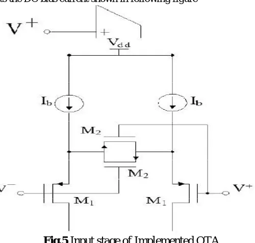
This is done in order to reduce the effects of lateral diffusion and to mitigate the problems of mismatch (Razavi, 2010). M1 transistors are used as the differential input pair; the M2 transistors are called the symmetrical diffuser, which are responsible for the improvement of the linear response of the output current as explained by Krummenacher (1988); the transistors M3 form the current mirrors that scale the trans conductance of the circuit and the transistors M5 are used to copy one of the branches of current in the other side to obtain a device of unique termination. The output trans conductance Gm can be expressed, very approximately, by the following equation: Gm =
( × ) (I)
where m represents the scaling factor due to the lower current mirror, while gm1 and gm2 represent the trans conductance of the transistors M1 and M2 of above Figure respectively. Other equations commonly involved in hand-computed CMOS analog design are shown in the following set (Tsividis, 2012, Banu, 2009). These equations are derived from the EKV model (model intended for circuit simulations and analog circuit design) and apply to all operating regions of the transistors:
= ∅ × ( ) (II)
( ) = 1 + 0.5√ + (III)
= (IV)
where Ibi represents the DC bias current shown in following figure
Fig.5 Input stage of Implemented OTA
Izi is the normalization current, μ, Cox and n are manufacturing technology parameters, W / L represents the
dimensions of the transistors and φt is the thermal voltage. From the above equations it can be observed that when the
engineer has to satisfy specific requirements within the objectives, it is necessary to take into account many different parameters during the design process. The usual design procedure is to modify some circuit values (such as transistor dimensions) and then adjust the rest of the parameters to meet the requirements. However, sometimes this process takes several iterations of trial and error trials to optimize the results. Most of the simulations and experiments that were performed showed that the linear range ΔV is directly dependent on the bias current and the dimensions of the
transistors M1 and M2 of above figure.
VI.GM-C FILTERS: SUMMARY AND CONSIDERATIONS ON YOUR SLEW RATE
A. Gm-C Filters:
OTAs are especially used in filters with very large time constants, which require high resistance or very low capacity (Arnaud, 2014). The OTA presented in above figure was used in the design of a first-order filter, as shown in following figure.
The objective of this filter is to obtain a basic and simple unit, which can be replicated in order to implement a more complex structure. The filter transfer function is as shown in the following equation:
=
( ) (VI)
and the pole where the cut off frequency is found is defined as:
= (VII)
B. SLEW RATE:
Another important parameter in filter design is its slew rate, as it can affect the actual filter bandwidth performance. It is defined as the maximum rate of change in the output voltage that the filter can deliver. If any input signal requires a higher rate, then the filter will not be able to produce the correct output response. This reason (SR) for a Gm-C filter is defined as (Razavi, 2010):
− = ⋮ = ⋮ (VIII)
The maximum possible output current is obtained when both values of Ib are directed to the output node. These currents can be scaled by the mirrors as well, so equation (10) represents the calculation of the rate of rise for the filter shown in the above figure:
− =2 × × (IX)
By combining equations (8) and (10) it is possible to define the response rate in terms of OTA variables and the desired cut off frequency fc (=wc/2π).
VII.DESIGN SPECIFICATIONS
The initial design of the OTA used 3μm / 8μm unit transistors for the entire circuit and a Ib of 26nA, in order
to obtain a trans conductance of 34n . The aim of the tool was to reduce the trans conductance value and input capacity of the OTA and at the same time increase the linear range to at least ± 500 mV.
The slew rate of the circuit should be 2.75 mV / μs for the correct operation of the filter in which this OTA will be
applied. In order to achieve this, the optimization tool has worked with the following circuit parameters: Ib, L1, L2, L3, L5, W1, W2, W3 and W5. The above figure presents the block diagram of the optimization tool designed to solve the problem in question. The objectives imposed by running the tool were: a) to increase the linear range and speed of response, and b) to decrease both the input capacity and the trans conductance.
VIII.GENETIC ALGORITHMS FOR MULTI OBJECTIVE OPTIMIZATION OF CIRCUITS
The aggregate fitness function F for a circuit A with a parameterization u is defined as:
( ) =∅( ( ), ( ), … , ( )) (X)
where each individual fitness function fi(Au) is defined as monotonically increasing with the fitness describing
the behavior of the circuit. In other words, the genetic algorithm optimizes the fitness parameters by looking for the highest possible value for each of them. So for this case it was necessary that the linear range and the rate of rise were as high as possible, and therefore their respective fitness values were directly proportional. In contrast, the input capacity and the trans-conductance should be as low as possible, and therefore their aptitude values were inversely proportional (Corne & Knowles, 2010).
IX.CONCLUSION
This work presents the application of an automated strategy with multi objective optimization to design and improve an OTA circuit. The EDA (Electronic Design Automation) tool is intended to help in the setting up of the circuit and the improvement process through the generation of optimized parameterizations.
This mechanism not only greatly reduces the time needed to design and simulate this type of circuit but also allows an optimal solution. Hand-based calculation design lags behind these advantages, even with less precision than automated tools. However, the best selection criteria remain the designer's job, as the Pareto front offers a map of optimized points.
A comparison of the values shows how the EDA tool has effectively improved the operation of the circuit in every aspect that is intended to be achieved.
REFERENCES
[1]. Arnaud, A. (2014). Very large time constant gm-c filters. (Tesis Doctoral). University of Uruguay.
[2]. Baru, M. (2009). Analog design methodologies when every nano ampere counts. CMOS Workshop Vancouver.
[3]. Corne, D. & Knowles, J. (2010). The Pareto envelope-based selection algorithm for multi objective optimization. PPSN VI: Proceedings of the International Conference on Parallel Problem Solving from Nature, 839-848.
[4]. Hassan, H., Anis, M. & Elmasry, M. (2005). MOS current mode circuits: analysis, design, and variability. IEEE Trans. VLSI Syst, 13(8): 885-898.
[5]. Krummenacher, F. & Joehl, N. (2008). A 4-mhz CMOS continuous time filter with on-chip automatic tuning. IEEE J. Solid-State Circuits, 23(3): 750-758.
[6]. MacEachern, L.A. (2009). Constrained circuit optimization via library table genetic algorithms. Proc. IEEE Int. Symp. Circuits and
Systems ISCAS ’99, 6, 310-313.
[7]. Lewinsky, A., & Silva-Martinez, J. (2004). OTA linearity enhancement technique for high frequency applications with IM3 below -65
dB. IEEE Transactions on Circuits and Systems-II: Express Briefs, 51(10), 542–548.
[8]. Nedungadi, A. & Viswanathan, T. (2004). Design of linear CMOS trans-conductance elements. IEEE Trans. Circuits Syst, 31(10): 891-894.
[9]. Razavi, B. (2010). Design of Analog CMOS Integrated Circuits. McGraw-Hill. Science/Engineering/Math.
[10]. Tsividis, Y. (2012). Mixed Analog-Digital VLSI Devices and Technology. Columbia University, USA: World Scientific Publishing. [11].Gregorian, R. and Temes, G.C, Analog MOS Integrated Circuits for signal processing, New York: Wiley, 1986.
[12].Vittoz, E.A, Micro power Techniques. In Tsividis, Y. and Antognetti, P. (eds), Design of MOS VLSI Circuits for Telecommunications. Englewood Cliffs, NJ: Prentice Hall, 1985b.
[14].Sougata Kumar Kar, Siddhartha Sen, A highly linear CMOS trans-conductance amplifier in 180 nm process technology, Analog Integrated Circuit Sig Process (2012) 72:163–171.
[15].Sinencio, E. S. Operational trans-conductance amplifiers (OTAs): A tutorial, Analog and Mixed Signal Center, TAMU.
[16].Texas Instruments, LM13700 Dual Operational Trans-conductance Amplifiers with Linearizing Diodes and Buffers, SNOSBW2F –November 1999–Revised November 2015.