Synthesis and Experimentation of Voltage Compressor and
Decompressor with Active Circuit
Qizheng Ji1, Lili Wu2, Jian Wang2, Fayu Wan2, *, and Blaise Ravelo2
Abstract—This paper introduces an innovative circuit theory of analog voltage compressor (AVC) and decompressor (AVD). This electronic function can also be assumed as an analog voltage converter. Analytically, it acts as power function synthesizer topology designed with an analog nonlinear circuit. The AVC/AVD topologies are based on an operational amplifier associated with resistor and non-linear diode components. Given the positive parametera >0, the mainx-y characteristic of the AVC/AVD is formulated by y =xa for the input and output x and y, respectively. The synthesis formulas allowing to determine the AVC/AVD parameters as a function of a are established. To validate the original AVC/AVD concept, static and dynamic simulations and experimentations with a proof-of-concept circuit using operational amplifier UA741 are carried out. As expected, well correlated x1/2-AVC andx2-AVD characteristics are realized with the static testing for the voltage range varied from 0 to 9-V and 0 to 3-V for AVC and AVD circuits, respectively. The simulation and experimentation of dynamic test results are in good agreement for the sine wave voltages with frequency varied from DC to 1-kHz. The simulated and experimental results confirm the relevance of the developed compressor/decompressor analog circuit. The AVC/AVD functions for instrumentation system applications can be potentially applied to the amplitude matching especially for digital systems.
1. INTRODUCTION
Nowadays, behind the technological progress, the instrumentations of modern embedded equipment as in aircraft [1, 2] and automobile [3, 4] systems become more and more complex. Various types of mechanical, hydraulic, magnetic, and electrical instrumentations can be found in systems [5–8]. The diagnosis and fault analyses of those systems require advanced electronic functions [9, 10]. The constituted electronic systems are usually designed with cohabitation of mixed low- and high-power electronic circuits [11]. To meet the expected standards, different specifications including unexpected transient phenomena must be fulfilled [12]. The electrostatic discharge (ESD) and electromagnetic interference (EMI) [13– 15] constitute high voltage effects that tend to appear in the low power and digital circuitries. The identification and measurement of these transient effects remain a challenging task for the design and manufacturing engineers [16].
To ensure the functionality notably with the online control and cyber systems [8, 17, 18], adequate interfaces enabling matching the signal level dynamics are necessary. Among proposal solutions against this technological challenge, we would suggest innovative compression and decompression functions applied to analog signal voltages.
Received 24 July 2019, Accepted 28 September 2019, Scheduled 11 October 2019
* Corresponding author: Fayu Wan ([email protected]).
1 Beijing Orient Institute of Measurement and Test, Beijing 100094, China.2Nanjing University of Information Science & Technology
1.1. State of the Art About the Voltage Compressor and Equivalent Electronic Function
Further attention in terms of reliability, robustness, and integrity must be paid to this technological progress [19, 20]. The technological constraints can be linked to the fabrication material as conductors, system complexity, or signal distortion. These critical points play on the performances of analog and digital electronic sensors and receiver-transmitter system [21, 22]. Different design solutions as mixed mode combination [21], implementation of switched-current analog RAM [22], and low-power high number of bits ADC/DAC [23] were proposed. Innovative architecture of configurable 802.11 standard transmitter has been recently introduced [24]. In addition to these digital and mixed functions, improvement was also made on the analog electronic function as amplifier and attenuator [25] for the dynamic signal amplitude matching. Variable and regulated attenuators were introduced to ensure the signal level matching [26–28]. Different technologies of attenuator with parameters control in frequency-and time-domain were invented last two decades [28–34]. Those inventions require further research work facing the issues of signal and power integrity [35–37]. However, so far, most of technological solutions for digital or mixed circuit interface signal level mismatching focused on the familiar concepts, such as the classical function (amplifier, attenuator, phase shifter, delay line . . . ) [21–37].
1.2. Need for Innovative Voltage Compressor
Traditionally, with the spectacular development of digital circuit technology, the electronic functions transmute more and more into numerical functions. However, numerical functions are dedicated to operate with a steady state level of voltage corresponding to “1” logic state by assuming that “0” corresponds to GND level. However, the electronic signals usually vary continuously and instantaneously in different ranges of values. This limitation requires an improvement which can be performed with analog voltage compression (AVC) and decompression (AVD) circuits by using for example compressor or decompressor.
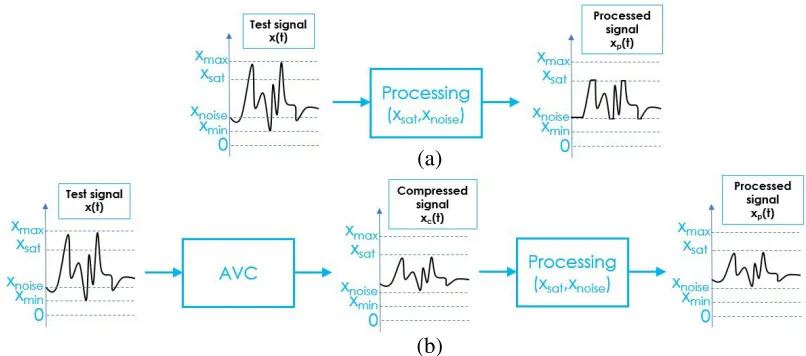
The main purpose of the present paper is to develop an original electronic function named analog voltage compression (AVC). This innovative electronic function allows matching high- and low-voltages. As illustrated in Fig. 1, it can be a solution to match the operating analog signal x(t) having dynamic range |xmax-xmin| with a digital processing circuit with saturation and noise resolution respectively
denoted as xsat and xnoise. As shown in Fig. 1(a), the processed signal xp(t) can be distorted because
of digital processing circuit voltage limitation. To avoid this technological issue, the AVC function can be interfaced between the input signal and digital circuit as seen in Fig. 1(b).
(a)
(b)
1.3. Outline of the Paper
The paper is mainly organized in five main sections. First, Section 1 introduces the state of the art and the main objective of the paper. Section 2 describes why the AVC and AVD functions can be useful for interfacing digital electronic circuit and outrange voltage signals. Section 3 is focused on the theoretical description of the AVC and AVD analog electronic function. The circuit synthesis method and implementation of the AVC and AVD are developed. To validate the AVC and AVD functions, proof-of-concept (POC) PCBs are designed and fabricated. The validation results with static and dynamic testings are discussed in Section 4. Last, Section 5 is the conclusion.
2. GENERAL DESCRIPTION OF THE PROPOSED ANALOG VOLTAGE COMPRESSOR (AVC) AND DECOMPRESSOR (AVD) FUNCTIONS
The present section describes the basic utility of the innovative AVC and AVD functions. It is introduced that these electronic functions can be used for the correction of signal amplitude mismatching.
2.1. Principle of AVC Function
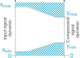
The AVC function principle is to shift the amplitude of analog voltage in order to reduce the maximal value. The diagram of Fig. 2 represents this amplitude variation principle by supposing the input and output signalsx(withxmin >0) andy. It enables reducing the input signal dynamic from|xmax−xmin|
into the compressed signal dynamic|ymax−ymin|.
Figure 2. Illustrations of the AVC function principle.
2.2. Diagrams of Signal Amplitude Levels through AVC and AVD Functions
The AVC and AVD operations can be explained with the budgets of signal levels. x(t) andy(t) represent the input and output test signals. Fig. 3(a) and Fig. 3(b) represent the budgets of the associated time dependent signal budget respectively. The AVC operation is characterized by the inequality
|xmax−xmin|>|ymax−ymin|. In contrary to the AVC, the AVD function increases the signal dynamic |xmax−xmin|<|ymax−ymin|.
2.3. Forecasted Applications of AVC and AVD Functions
As aforementioned in the previous section, the AVC and AVD functions are intended to interface analog voltages with digital circuits. Fig. 4 depicts the signal level budget with the configuration of this technological solution. It consists in cascading an AVC-digital-AVD circuit. The AVC transforms the input transient signal x(t) into xc(t) in order to operate in the digital circuit dynamic range
(a) (b)
Figure 3. Diagrams of signal level budget: (a) AVC and (b) AVD.
Figure 4. Diagram of signal level budget through an AVC-digital circuit-AVD chain.
3. THEORY ON THE PROPOSED AVC AND AVD
This section introduces the established circuit theory on the innovative AVC and AVD functions. The topological cell enabling the realization of the introduced signal compression is analyzed. The voltage convertorx-ycharacteristics of the circuit are elaborated. Then, the AVC and AVD design and synthesis methods are proposed.
3.1. Analytical Definition of the Proposed AVC and AVD Functions
Let us denote the time-dependent signals x(t) >0 and y(t) as real time-dependent variables, andα is real positive constant. The basic principle of the proposed synthesizer is based on the power function. In analytical point of view, the AVC and AVD functions or x-y characteristics are defined by the mathematical function:
y(t) = [x(t)]a. (1)
withαbeing a real positive function. Knowing the exponential and logarithmic properties, this equation can be rewritten as:
y(t) = exp [lnx(t)a], (2)
or
y(t) = exp [alnx(t)]. (3)
Based on the system theory, Equation (3) can be implemented by cascading three elementary block functions as depicted in Fig. 5.
Figure 5. Equivalent diagram of Equation (1).
3.2. Elementary Cells for Logarithm and Exponential Voltage Based Functions
The exponential function described in Eq. (3) can be synthesized and implemented as an analog circuit constituted by two basic analog circuit cells. On one hand, it can be realized by exploiting the bipolar junction semiconductor diode D presenting a general I-V (current-voltage) characteristic and analytically defined as:
i(t)≈I0exp
v(t)
nVT
, (4)
with:
• nis the ideality factor, also known as the quality factor or sometimes emission coefficient,
• VT = 26 mV at the room temperature usually 25◦C is the thermal voltage de pending on the diode material properties,
• AndI0 is the reverse bias saturation current (or scale current).
On the other hand, it can also be generated from a current-to-voltage convertor with an arbitrary resistor R (chosen in function of the input current sensitivity) and an operational amplifier-based cell generating the function:
y(t) =R·i(t). (5)
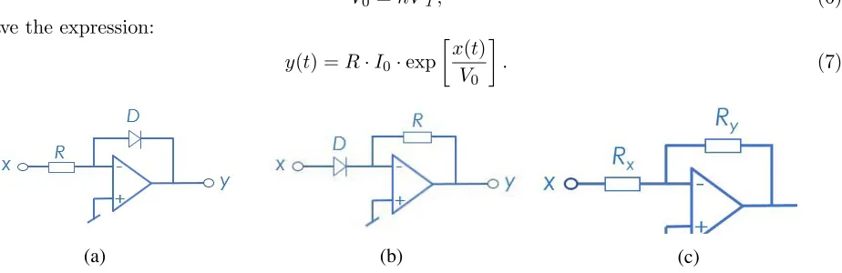
Therefore, with an ideal operational amplifier, the exponential function can be implemented with the basic circuit presented in Fig. 6(a). By denoting x(t) =v(t),
V0=nVT, (6)
we have the expression:
y(t) =R·I0·exp
x(t)
V0
. (7)
(a) (b) (c)
Figure 6. Topology of elementary cells: (a) exponential, (b) logarithm, (c) inverter amplifier.
The inverse of this equation corresponds to the reciprocal exponential function which is a logarithmic function and can be generated by permuting the resistor and diode as presented in Fig. 6(b). The characteristic equation is expressed as:
y(t) =−V0ln
x(t)
R·I0
. (8)
The amplifier function can be realized with an operational amplifier-based inverter or a non-inverter cell. Fig. 6(c) shows the circuit schematic. According to the circuit theory, this classical linear function:
y(t) =a·x(t) =−Ry
Rxx(t), (9)
3.3. Topological Analysis of the AVC and AVD Circuits
As aforementioned, the AVC and AVD functions are analytically power functions. The basic principle of the developed typically voltage convertor topologies is inspired from the mathematical concept:
• The AVC can be ideally realized with the system sketched in Fig. 5 whena <1;
• And on the other hand, this system behaves as an AVD whena >1).
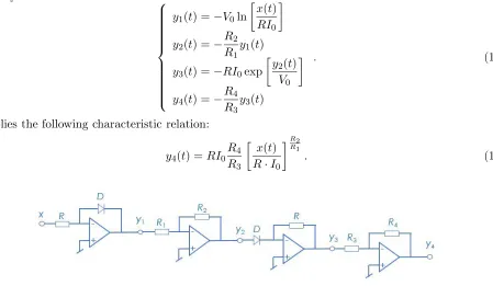
As pointed out in Equation (1) and shown in Fig. 5, the functiony(t) = [x(t)]2 can be implemented by cascading logarithmic and exponential cells. Fig. 7 represents the yielded configuration of the power function topology. The considered topology of power function is composed of logarithm cell, first amplifier cell, and cell exponential in cascade. By assuming the operational amplifier as ideal, we have the analytical characteristic: ⎧
⎪ ⎪ ⎪ ⎪ ⎪ ⎪ ⎪ ⎪ ⎪ ⎨ ⎪ ⎪ ⎪ ⎪ ⎪ ⎪ ⎪ ⎪ ⎪ ⎩
y1(t) =−V0ln
x(t)
RI0
y2(t) =−RR2 1y1
(t)
y3(t) =−RI0exp
y2(t) V0
y4(t) =−RR4 3y3
(t)
. (10)
It implies the following characteristic relation:
y4(t) =RI0R4 R3
x(t)
R·I0 R2
R1
. (11)
Figure 7. Implementation of the power function.
In order to get the targeted characteristic introduced in Eq. 1), the pre- and post-conditioning
correction factors: ⎧
⎪ ⎨ ⎪ ⎩
Cx=val(R·I0) = RR2 1
Cy =val(R·I0) =R4 R3
, (12)
are added at the input and output of the circuit shown in Fig. 7. It acts as a no-unit factor, expressing the value of the voltage, here written by the function val(·), to equalize the diode intrinsic parameters
V0 and I0. The resistances R1,R2,R3, and R4 can be synthesized with the following relations:
R2 =val(RI0)·R1 R4 =val(RI0)·R3 .
(13)
Then, the resistanceRy can be calculated fromRx with the following relation:
Ry =a·Rx. (14)
It is noteworthy that under the decompression operation, to avoid the last stage operational amplifier saturation (x(t)< Vcc), the input signal must be lower than:
x(t)≤Vmax=RI0exp VVcc 0
To check the effectiveness of the developed theory, the next section presents illustrative application examples. Design, simulation, and experimentations of proof-of-concept will be described. The feasibility of the proposed synthesizer will be verified with static and dynamic signal testing.
4. SIMULATIONS AND EXPERIMENTAL VALIDATIONS OF THE AVC AND AVD FUNCTIONS
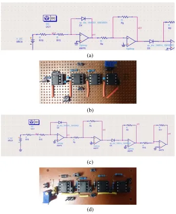
The present section is focused on the design, fabrication, simulation, and experimental validations. The POC circuit is designed with lumped components, resistance R and diode D, and the operational amplifier UA741 from Texas InstrumentsR. The simulated results run in the SPICE ADSRenvironment of the AVC and AVD circuits are compared with time-domain measurements.
(a)
(b)
(c)
(d)
4.1. Description of the POC Circuits
To perform the experimental testings, classical lumped resistors, diodes, and operational amplifiers are implemented on a FR4 dielectric substrate. The specifications of the components constituting the AVC and AVD circuit POCs are shown in Table 1. Fig. 8 present the schematic and photo of the tested AVC and AVD POC circuits, respectively. The AVC and AVD PCB circuits act as low frequency PCBs with classical wire interconnections. The POC-modeled computed results are compared with simulations run in the ADSRenvironment of the electronic circuit designer and simulator. The proposed
x-y characteristics and time domain simulations are performed. Comparisons of thex-y characteristics results for the ideal theory, ADS simulation, and measurement are presented. The obtained time domain simulation results will be explored in the next paragraphs.
Table 1. Specifications of the AVC and AVD components.
Description References Parameters Manufacturer
Amplifier operational UA471R - Texas InstrumentsR
R - 1 kΩ MurataR
R1 - 1 kΩ MurataR
R2 - 2 kΩ MurataR
R3 - 1 kΩ MurataR
R4 - 1 kΩ MurataR
D N4002 - Texas InstrumentsR
The lumped elements are implemented on an FR4-epoxy substrate. The signal interconnect accesses are realized with BNC connectors.
4.2. Discussions on the Validation Results
To validate the AVC and AVD topologies, comparisons among the ideal calculations, SPICE simulations, and experimental measures are described in this subsection.
4.2.1. Experimental Test Protocols
Fig. 9(a) represents the block diagram of the experimental test protocol. Fig. 9(b) illustrates the connections between the measurement equipment and the circuit under test (CUT).
The input test voltages are provided with the arbitrary wave generator (AWG) AgilentR33220A. The CUT is fed by +/−Vcc = +/−15 V and 30 mA with the DC power supply KeysightRE3631A. The test signals are plotted and recorded with the digital oscilloscope AgilentRDSO9404A having 4 GHz
bandwidth and 20 GSamplings/s sampling rate. All the test results explored in this paper are obtained with transient signals representing the input and output signals.
4.2.2. x-y Characterization Results
The AVC and AVD x-y characterizations are carried out by considering saw tooth wave input signals. The AVCx1/2 characteristic is generated with the transient signalx which presents period T1 = 10 ms
and amplitude xmax = 9 V. Fig. 10 displays the comparisons between the ideal, simulated (“simu.”),
(a) (b)
Figure 9. Experimental setup: (a) Illustrative diagram and (b) Photo.
2 4 6 8
0 1 2 3 4 y ( V ) x (V) Ideal Simu. Meas.
0.5 1 1.5 2 2.5 3
-5 0 5 10 15 y ( V ) x (V) (a) (b)
Figure 10. Comparison of calculated (“ideal”), simulated (“simu.”) and measured (“meas.”) x
-y characteristics of POC circuits: (a) AVC, (b) AVD.
0 5 10 15 20
-2 0 2 4 6 8 10 12 Vo lt a g e ( V ) Time (ms)
x xc
simu.
x c
meas.
0 5 10 15 20
-2 0 2 4 6 8 10 12 Vo lt a g e ( V ) Time (ms) (a) (b)
Figure 11. Comparison between simulation and measurement of POC dynamic test results with arbitrary signals: (a) AVC and (b) AVD.
The AVD characteristic is generated with the transient signalxwhich presents periodT1 = 100 ms
and amplitudexmax= 3 V. Fig. 10(b) monitors the AVD comparative results. As pointed out in Fig. 10,
Therefore, the simulations and experimentations confirm the developed AVC and AVD circuit theory. For both AVC and AVD circuits, the notable slight deviations among the three curves are mainly due to imperfections of the components especially the operation amplifier UA741, AWG parasitic, and scope numerical inaccuracies.
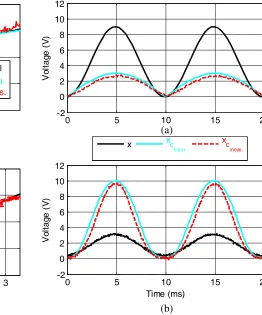
4.2.3. Dynamic Test Results with Sine Waveform Signals
The dynamic test validations are realized with sine wave form signals with frequencies from DC to 1 kHz. Fig. 11(a) explains the feasibility of the voltage compression effect by considering the voltage sine signal with periodT1 = 10 ms, peak-to-peak amplitude equal to aboutxpp = 9 V, and average value
4.5 V. Furthermore, Fig. 11(b) confirms the voltage decompression effect. In this case, input voltage with same period but lower peak-to-peak amplitude about 3 V is considered to avoid the saturation effects. It can be pointed out that the compressed and decompressed voltages xc are a periodical non-sine signal because of the nonlinear aspect of the AVG. They present the same dynamic of variation as forecasted in the previous paragraph. The average difference about ΔV= 0.2 V between the simulation and measurement is mainly due to the offset of the operation amplifier UA741. For both cases of CUT, the simulations and measurements are in very good agreement.
4.2.4. Dynamic Test Results with Arbitrary Waveform Signals
For the further general insight about the developed AVC and AVD functions, two different arbitrary waveform signals are tested.
Figure 12 displays the dynamic test results with sinc waveform signals. Two different pulse durations about 2 ms (in top) and 1.2 ms (in bottom) are shown in these figures. For both results, the sinc signal amplitudes are reduced from about xpp = 7.7 V to xc pp = 2 V through the AVC function. Then, the compressed signals are reconstructed keenly thanks to the AVD operation. Fig. 13 presents
0 2 4 6 8 10
0 2 4 6 8 Vo lt a g e ( V ) Time (ms) x x c yc y
0 0.5 1 1.5 2 2.5 3
0 2 4 6 8 V o lt ag e ( V ) Time (ms) (a) (b)
Figure 12. AVC and AVD measurement results with 2 ms (in top) and 1.2 ms (in bottom) pulse width sinc waveform signals.
0 1 2 3 4 5 6
-2 0 2 4 6 8 V o lt ag e ( V ) Time (ms) x xc yc y
0 0.5 1 1.5 2
-2 0 2 4 6 8 Vo lt a g e ( V ) Time (ms) (a) (b)
the results of cardiac waveform signal testings. In top (resp. bottom) of this figure, the test signal presents a pulse duration about 1.5 ms (resp. 0.7 ms). Once more, it can be emphasized that the signal level dynamic is reduced from about xpp = 6 V to xc pp = 2 V. The arbitrary test results confirm the possibility of AVC and AVD function complementarity. The slight deviations between the initial and reconstructed signals are mainly due to the apparatus numerical noises and imperfections of the components used to fabricate the AVC and AVD circuits.
5. CONCLUSION
An original circuit theory on the AVC and AVD electronic functions is developed. The circuit topologies are typically analog nonlinear circuits presentingx-ycharacteristic as mathematical power function. The operation and design principle are described. The proposed AVC and AVD function synthesizer is based on the cascade of logarithm, and exponential cells are developed. The basic cells generating the power function are analyzed.
Two POC circuit prototypes are designed and fabricated to validate the AVC and AVG concepts. Thex-y characteristics and dynamic responses of the CUT are investigated. Thex2 andx1/2 functions are tested with 8-Vcc amplitude sine signals. As expected, very good correlations among the expected
model, SPICE simulations, and experimental results are obtained. In addition, the functions are validated with arbitrary signals presenting sinc and cardiac waveforms milliseconds pulse duration.
In the continuation of this study, the proposed AVC and AVG functions will be applied to the interfacing numerical circuits as microcontroller unit board. This technological solution can be a good candidate for the future technology as the amplitude matching low voltage digital circuits [39, 40].
ACKNOWLEDGMENT
This research work was supported jointly by NSFC (61971230 and 61601233), the Electrostatic Research Foundation of Liu Shanghe Academicians and Experts Workstation, Beijing Orient Institute of Measurement and Test (BOIMTLSHJD20181003), Jiangsu Innovation and Enterprise Group Talents Plan 2015 (SRCB201526) and PAPD.
REFERENCES
1. Aircraft instruments and avionics, http://sarasotaavionics.com/category/flight-instruments, ac-cessed 5 Dec. 2018.
2. Instrument Flying Handbook (FAA-H-8083-15B) Note, 2012, https://www.faa.gov/regulations policies/handbooks manuals/aviation/media/FAA-H-8083-15B.pdf, accessed 1 Dec. 2018.
3. Measuring Instruments for the Automotive Market, 2014, http://hiokiusa.com/wp-content/ uploads/pdf/18033-Chirasi mobileE3-42M.pdf, accessed 1 Dec. 2018.
4. Quick Guide to Precision Measuring Instruments, E4329, 2003, https://www.mitutoyo.co.jp/eng/ pdf/E4329 QuickGuide.pdf, accessed 1 Dec. 2018.
5. Rubio, J. J., J. Pieper, J. A. Meda-Campa˜na, A. A. Aguilar, V. I. Rangel, and G. J. Gutierrez, “Modelling and regulation of two mechanical systems,”IET Science, Measurement & Technology, Vol. 12, No. 5, 657–665, 2018.
6. Rong, H., L. Ling Zou, C. Peng, J. Lv, Y. Chen, and Y. Zhu, “Adaptive regulation of the weights of REQUEST used to magnetic and inertial measurement unit based on hidden Markov model,”
IET Science, Measurement &Technology, Vol. 12, No. 5, 666–672, 2018.
7. Igder, M. A., T. Niknam, and M.-H. Khooban, “Bidding strategies of the joint wind, hydro, and pumped-storage in generation company using novel improved clonal selection optimisation algorithm,”IET Science, Measurement & Technology, Vol. 11, No. 8, 991–1001, 2017.
9. Ahour, J. N., S. Seyedtabaii, and G. B. Gharehpetian, “Determination and localisation of turn-to-turn fault in transformer winding using frequency response analysis,” IET Science, Measurement
& Technology, Vol. 12, No. 3, 291–300, 2018.
10. Rajamani, R., M. Rajappa, K. Arunachalam, and B. Madanmohan, “Interturn short diagnosis in small transformers through impulse injection: on-line on-load self-impedance transfer function approach,”IET Science, Measurement &Technology, Vol. 11, No. 8, 961–966, 2017.
11. Mpitziopoulos, A., “PSUs 101: A detailed look into power supplies,” 2015, https://www. tomshardware.com/reviews/power-supplies-101,4193-9.html. accessed 1 Dec. 2018
12. Jordan, A., “Meeting transient specifications for electrical systems in military vehicles,”Application Note, VICOR, http://cdn.vicorpower.com/documents/application notes/milvehicle appnote.pdf, accessed 1 Dec. 2018.
13. Cole, B., “Transients, ESD and EMI in an untethered world,” Nov. 2013.
https://www.embedded.com/electronics-blogs/cole-bin/4424828/Transients–ESD-and-EMI-in-an-untethered-world, accessed 1 Dec. 2018.
14. Don Russell, B., M. Stu, H. Stig, and N. Stig, “Substation electromagnetic interference, Part I: Characterization and description of the transient EMI problem,” IEEE Transactions on Power Apparatus and Systems (PER), Vol. 4, No. 7, 1863–1870, 1984.
15. “Meeting military requirements for EMI and transient voltage spike suppression DC-DC converters and accessories,” Application note, AN0041.0, 1–13, http://www.vptpower.com/wp- content/uploads/downloads/2017/06/Meet-Mil-Req-EMI-and-transient-v-spike-suppression-AN004-1.pdf, accessed 1 Dec. 2018.
16. Lepkowsk, J., “Identification of transient voltage noise sources,” Rev. 0, Semiconductor Components Industries, AND8228/D, 2005, http://www.onsemi.com/pub/Collateral/AND8228-D.PDF, accessed 1 Dec. 2018.
17. Xue, G., “End-to-end data paths: Quickest or most reliable?,” IEEE Communications Letters, Vol. 2, No. 6, 156–158, 1998.
18. Fan, X., L. Li, Y. Zhou, N. Tang, Z. Zou, X. Li, G. Huang, and M. Liu, “Online detection technology for SF6 decomposition products in electrical equipment: A review,”IET Science, Measurement &
Technology, Vol. 12, No. 6, 707–711, 2018.
19. Kapur, P., G. Chandra, J. P. McVittie, and K. C. Saraswat, “Technology and reliability constrained future copper interconnects — Part II: performance implications,” IEEE Trans. Electron Devices, Vol. 49, No. 4, 598–604, 2002.
20. Tripathi, J. N., R. K. Nagpal, and R. Malik, “Robust optimization and reflection gain enhancement of serial link system for signal integrity and power integrity,” Int. J. of Design, Analysis and Tools for Circuits and Systems, Vol. 2, No. 1, 70–85, 2011.
21. Cordeiro, R. F., S. R. Oliveira Arnaldo, and J. M. N. Vieira, “All-digital transmitter with a mixed-domain combination filter,”IEEE Trans. Circuits Syst. II Exp. Briefs, Vol. 63, No. 1, 4–8, 2016. 22. Sharma, S. and T. Ytterdal, “In-probe ultrasound beamformer utilizing switched-current analog
RAM,”IEEE Trans. Circuits Syst. II Exp. Briefs, Vol. 62, No. 6, 571–521, 2015.
23. Jeon, B.-K., S.-K. Hong, and O.-K. Kwon, “A low-power 12-bit extended counting ADC without calibration for CMOS image sensors,” IEEE Transactions on Circuits and Systems II: Express Briefs, Vol. 65, No. 7, 824–828, 2018.
24. Gebreyohannes, F. T., A. Frapp´eand, and A. Kaiser, “A Configurable Transmitter Architecture for IEEE 802.11ac and 802.11ad Standards,”IEEE Transactions on Circuits and Systems II: Express Briefs, Vol. 63, No. 1, 9–13, 2016.
25. Tadi´c, N., A. Dervi´c, M. Erceg, B. Goll, and H. Zimmermann, “A 54.2 dB current gain dynamic range, 1.78 GHz gain-bandwidth product CMOS voltage-controlled current amplifier/attenuator,”
IEEE Transactions on Circuits and Systems II: Express Briefs, (early access), 824–828, 2018. 26. El-Gabaly, A. M. and C. E. Saavedra, “A quadrature pulse generator for short-range UWB vehicular
27. Stukach, O. V., “Modeling of attenuator structures on field effect transistors with minimal phase shift at attenuation regulation,”Power Engineering, Bulletin of the Tomsk Polytechnic University, Vol. 311, No. 4, 90–93, 2007.
28. Barta, “Automatic return-loss optimization of a variable FET attenuator,” Patent US4975604, 1990, patents.google.com/patent/US4975604, accessed 1 Oct. 2018.
29. Ehlers, E. R. and D. J. Dascher, “Broadband step attenuator with improved time domain per-formance,” Patent US20060279376, 2006, http://www.freepatentsonline.com/y2006/0279376.html, accessed 1 Oct. 2018.
30. Huang, F.-H. and J.-M. R. Mourant, “Analog control integrated FET based variable attenuators,” Patent US7205817,327/308, 2007, patents.google.com/patent/US7205817, accessed 1 Oct. 2018. 31. Hwang, H. S., Y. S. Na, M. S. Kim, B. H. Jo, and K. S. Park, “Step attenuator,” Patent US7525395,
2009, patents.google.com/patent/US7525395, 2009-04-28, accessed 1 Oct. 2018.
32. Vice, M. W., “Four-state digital attenuator having two-bit control interface,” Patent US7786822, 2010, patents.google.com/patent/US7786822, accessed 1 Oct. 2018.
33. Staudinger, “Electronic circuits with variable attenuators and methods of their operation,” Patent US8674746, 2014, patents.google.com/patent/US8674746, accessed 1 Oct. 2018.
34. Sharma, V., “Low phase shift, high frequency attenuator,” Patent US9787286B2, 2017, patents.google.com/patent/US9787286, accessed 1 Oct. 2018.
35. Buckwalter, J. F., “Predicting microwave digital signal integrity,” IEEE Trans. Adv. Packaging, Vol. 32, No. 2, 280–289, 2009.
36. Srivastava, M. B. and M. Potkonjak, “Optimum and heuristic transformation techniques for simultaneous optimization of latency and throughput,”IEEE Trans. Very Large Scale Integration (VLSI) Systems, Vol. 3, No. 1, 2–19, 1995.
37. Liu, W.-C., T.-C. Wei, Y.-S. Huang, C.-D. Chan, and S.-J. Jou, “All-digital synchronization for SC/OFDM mode of IEEE 802.15.3c and IEEE 802.11ad,” IEEE Trans. Circuits and Systems I: Regular Papers, Vol. 62, No. 4, 545–553, 2015.
38. Eudes, T. and B. Ravelo, “Analysis of multi-gigabits signal integrity through clock H-tree,”Int. J. Circ. Theor. Appl., Vol. 41, No. 5, 535–549, May 2013.
39. Hasanzadeh, M. R. and A. Abrishamifar, “A novel OTA compensation approach suitable for CT-ΔΣ modulators,” Int. J. Circ. Theor. Appl., Vol. 46, No. 12, 2248–2265, Dec. 2018.