SLOA068 – October 2001
Guidelines for Measuring Audio Power Amplifier
Performance
Audio Power Amplifiers ABSTRACTThis application note provides guidelines for measuring the data sheet parameters of Texas Instruments audio power amplifiers (APAs) using prefabricated evaluation modules (EVMs). The primary equipment used for the measurements consists of the System Two™ audio measurement system by Audio Precision™, a digital multimeter (DMM), and a dc power supply.
Contents
1 Introduction ...2
2 Basic Measurement System...3
3 Interfacing to the APA...5
3.1 Differential Input and BTL Output (TPA731 and TPA2000D1)...5
3.2 SE Input and SE Output (TPA0211 and TPA711)...6
3.3 Other Configurations ...7
3.4 Class-D RC Low-Pass Filter...7
4 Total Harmonic Distortion Plus Noise (THD+N) ...9
4.1 THD+N vs Output Power...10
4.2 THD+N vs Frequency...11
4.3 Maximum Output Power Bandwidth ...11
4.4 Maximum Input Voltage...11
5 Noise ...12
5.1 Integrated Noise vs Frequency ...12
5.2 Signal-to-Noise Ratio ...13
6 Gain and Phase ...13
7 Crosstalk...15
8 Supply Rejection ...17
9 Power Measurements and Related Calculations...21
9.1 Efficiency Measurements ...21
9.2 Power Dissipated vs Power to the Load...24
9.3 Crest Factor and Output Power...25
10 Measurement Pitfalls ...26
10.1 Effects of Improper Interfacing and Grounding ...26
10.2 THD+N Measurements...27
10.3 Noise Measurements ...27
10.4 Gain and Phase Measurements...28
10.5 Crosstalk Measurements...28
10.6 Supply Rejection Measurements...28
10.7 Efficiency Measurements ...28
Figures
Figure 1. Audio Measurement Systems: (a) Class-AB APAs and (b) Filter-Free Class-D APAs... 4
Figure 2. Differential Input—BTL Output Measurement Circuit ... 5
Figure 3. SE Input—SE Output Measurement Circuit ... 7
Figure 4. Measurement Low-Pass Filter Derivation Circuit—Class-D APAs ... 8
Figure 5. THD+N Measurement Circuit Using the AP-II Measurement System: Differential-BTL... 10
Figure 6. THD+N vs POUT for the TPA2001D1 and the TPA731 ... 10
Figure 7. THD+N vs Frequency for the TPA2001D1 and the TPA731 ... 11
Figure 8. Noise Measurement Circuit ... 12
Figure 9. Measured Results of Noise Circuit ... 13
Figure 10. Gain and Phase Measurement Circuit ... 14
Figure 11. TPA731 Gain and Phase Measurements ... 14
Figure 12. TPA2001D1 Gain and Phase Measurements... 15
Figure 13. Crosstalk Measurement Circuit... 16
Figure 14. Crosstalk Measurements... 17
Figure 15. PSRR and kSVR Measurement Circuit... 18
Figure 16. kSVR Filter Circuit... 19
Figure 17. kSVR of the TPA2001D1 and TPA731... 20
Figure 18. Impact of CBYPASS on kSVR for the TPA711 Class-AB APA ... 20
Figure 19. Efficiency Measurement Circuit for Class-AB and Class-D BTL APAs... 22
Figure 20. Efficiency Graphs of the TPA731 and TPA2001D1... 24
Figure 21. Graph of Power Dissipated vs Output Power ... 24
Figure 22. Supply and Output Power vs CF for the TPA731 and TPA2001D1 ... 26
Figure 23. Effect of Generator Interface on APA Measurements, THD+N vs Power Shown ... 27
Tables Table 1. Recommended Minimum Wire Size for Power Cables... 6
Table 2. Typical RC Measurement Filter Values ... 9
Table 3. Efficiency Data for the TPA731 and TPA2001D1 ... 23
Table 4. Power vs Crest Factor... 25
1 Introduction
The primary goal of audio measurements is to determine the performance of a device in the audible spectrum, 20 Hz to 20 kHz. Although most people do not hear frequencies below 50 Hz or above 17 kHz, the broad spectrum is an industry standard that allows a more accurate comparison of devices. The performance can be quickly analyzed, and only a few basic pieces of equipment are required.
A method for measuring standard data sheet information for audio power amplifiers (APAs) is presented for several key parameters. These are:
• THD+N versus output power • Crosstalk versus frequency
• THD+N versus frequency • Power supply rejection ratio
• Gain and phase versus frequency • Supply ripple voltage rejection ratio
• Integrated noise • Efficiency
The measurements in this application note were made using TI Plug-N-Play APA evaluation modules (EVMs). The TPA2001D1 and TPA731 mono devices were used for most
measurements. The TPA2001D2 and TPA0212 devices were used for the crosstalk measurements, which require a stereo device.
Note that the measurements are dependent upon the layout of the printed-circuit board (PCB), particularly with class-D APAs. The graphs in the data sheet reflect typical specifications and were measured on test boards specifically designed to allow accuracy and ease of
measurement. The measurements in this application note, however, were taken using circuits on EVMs that reflect real-world layout constraints. The measurements of a particular audio circuit may vary from the typical specifications. A large variance is usually indicative of a PCB layout or measurement system issue.
2
Basic Measurement System
This application note focuses on methods that use the basic equipment listed below:
• Audio analyzer or spectrum analyzer • Digital multimeter (DMM)
• Oscilloscope • Twisted pair wires
• Signal generator • Power resistor(s)
• Linear regulated power supply • Filter components
• EVM or other complete audio circuit
Figure 1 shows the block diagrams of basic measurement systems for class-AB and class-D amplifiers. A sine wave is normally used as the input signal since it consists of the fundamental frequency only (no other harmonics are present). An analyzer is then connected to the APA output to measure the voltage output. The analyzer must be capable of measuring the entire audio bandwidth. A regulated dc power supply is used to reduce the noise and distortion injected into the APA through the power pins. A System Two audio measurement system (AP-II)
(Reference 1) by Audio Precision includes the signal generator and analyzer in one package. The generator output and amplifier input must be ac-coupled. However, the EVMs already have the ac-coupling capacitors, (CIN), so no additional coupling is required. The generator output
impedance should be low to avoid attenuating the test signal, and is important since the input resistance of APAs is not very high (about 10 kΩ). Conversely the analyzer-input impedance should be high. The output impedance, ROUT, of the APA is normally in the hundreds of
milli-ohms and can be ignored for all but the power-related calculations.
Figure 1(a) shows a class-AB amplifier system, which is relatively simple because these
amplifiers are linear―their output signal is a linear representation of the input signal. They take analog signal input and produce analog signal output. These amplifier circuits can be directly connected to the AP-II or other analyzer input.
This is not true of the class-D amplifier system shown in Figure 1(b), which requires low pass filters in most cases in order to measure the audio output waveforms. This is because it takes an analog input signal and converts it into a pulse-width modulated (PWM) output signal that is not accurately processed by some analyzers.
Analyzer 20 Hz - 20 kHz (a) Basic Class-AB Audio Measurement System
APA Signal Generator Power Supply Analyzer 20 Hz - 20 kHz RL
(b) Filter-Free and Traditional Class-D Audio Measurement System Class-D APA Signal Generator Power Supply RL Low-Pass RC Filter Low-Pass RC Filter Low-Pass LC Filter
Used With Traditional Class-D APAs Only Used With Filter-Free Class-D APAs Only
Figure 1. Audio Measurement Systems: (a) Class-AB APAs and (b) Filter-Free Class-D APAs
Two types of class-D amplifiers exist: traditional class-D that requires a low-pass LC filter to produce an analog output, and TI’s new filter-free class-D which does not require a low-pass output filter for normal operation because the speaker provides the inductance necessary to achieve high efficiency.
Two families of class-D APAs (TPA032D0x, TPA005Dxx) use the traditional modulation scheme that requires the LC filter for proper operation. The data sheets, EVM manuals, and application notes (References 2 and 3) provide more information about this filter.
The filter-free class-D APA families (TPA2000Dx and TPA2001Dx) use a modulation scheme that does not require an output filter for operation, but they do sometimes require an RC low-pass filter when making measurements. This is because some analyzer inputs cannot accurately process the rapidly changing square-wave output and therefore record an extremely high level of distortion. The RC low-pass measurement filter is used to remove the modulated waveforms so the analyzer can measure the output sine wave.
3
Interfacing to the APA
This section describes the important points to be considered when connecting the test equipment to the APA. The first two subsections describe the connections to differential and single-ended (SE) APA inputs and outputs. The last subsection discusses the RC low-pass filter design that is sometimes required for filter-free class-D measurements.
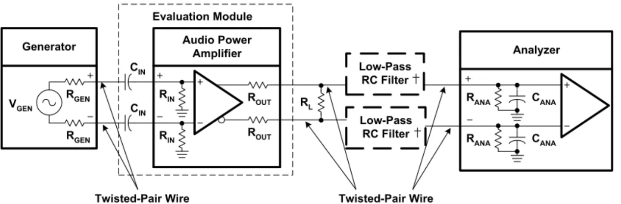
3.1 Differential Input and BTL Output (TPA731 and TPA2000D1)
All of the class-D APAs and many class-AB APAs have differential inputs and bridge-tied load (BTL) outputs. Differential inputs have two input pins per channel and amplify the difference in voltage between the pins. Differential inputs reduce the common-mode noise and distortion of the input circuit. BTL is a term commonly used in audio to describe differential outputs. BTL outputs have two output pins providing voltages that are 180 degrees out of phase. The load is connected between these pins. This has the added benefits of quadrupling the output power to the load and eliminating a dc blocking capacitor.
A block diagram of the measurement circuit is shown in Figure 2. The differential input is a balanced input, meaning the positive (+) and negative (-) pins will have the same impedance to ground. Similarly, the BTL output equates to a balanced output.
CIN Audio Power Amplifier Generator Low-Pass RC Filter CIN RGEN RGEN RIN RIN VGEN ROUT ROUT Analyzer RANA RANA CANA Low-Pass RC Filter RL CANA Twisted-Pair Wire Evaluation Module Twisted-Pair Wire
The RC low-pass filter is required only for measuring the filter-free class-D audio power amplifiers.
Figure 2. Differential Input—BTL Output Measurement Circuit
The generator should have balanced outputs and the signal should be balanced for best results. An unbalanced output can be used, but it may create a ground loop that will affect the
measurement accuracy. The analyzer must also have balanced inputs for the system to be fully balanced, thereby cancelling out any common mode noise in the circuit and providing the most accurate measurement.
The following general rules should be followed when connecting to APAs with differential inputs and BTL outputs:
• Use a balanced source to supply the input signal.
• Use an analyzer with balanced inputs.
• Use shielding when the system environment is noisy.
• Ensure the cables from the power supply to the APA, and from the APA to the load, can handle the large currents (see Table 1 below).
Table 1 shows the recommended wire size for the power supply and load cables of the APA system. The real concern is the dc or ac power loss that occurs as the current flows through the cable. These recommendations are based on 12-inch long wire with a 20-kHz sine-wave signal at 25°C.
Table 1. Recommended Minimum Wire Size for Power Cables
PO UT(W) RL (Ω) AWG Size DC Power Loss (mW) AC Power Loss (mW) 10 4 18 22 16 40 18 42 2 4 18 22 3.2 8.0 3.7 8.5 1 8 22 28 2.0 8.0 2.1 8.1 < 0.75 8 22 28 1.5 6.1 1.6 6.2
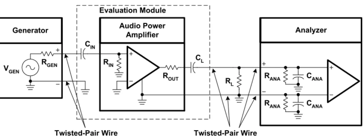
3.2 SE Input and SE Output (TPA0211 and TPA711)
The SE input and output configuration is used with class-AB amplifiers only. A block diagram of a fully SE measurement circuit is shown in Figure 3. Fully SE APAs are, in general, headphone or headset amplifiers, though the TPA0211 and TPA711 are APAs with SE capability. SE inputs normally have one input pin per channel. In some cases two pins are present; one is the signal and the other is ground. SE outputs have one pin driving a load through an output ac coupling capacitor and the other end of the load is tied to ground. SE inputs and outputs are considered to be unbalanced, meaning one end is tied to ground and the other to an amplifier input/output. The generator should have unbalanced outputs, and the signal should be referenced to the generator ground for best results. Unbalanced or balanced outputs can be used when floating, but they may create a ground loop that will effect the measurement accuracy. The analyzer should have balanced inputs to cancel out any common-mode noise in the measurement.
CIN Audio Power Amplifier Generator RGEN RIN VGEN ROUT Analyzer RANA RANA CANA RL CANA Twisted-Pair Wire Evaluation Module Twisted-Pair Wire CL
Figure 3. SE Input—SE Output Measurement Circuit
The following general rules should be followed when connecting to APAs with SE inputs and outputs:
• Use an unbalanced source to supply the input signal.
• Use an analyzer with balanced inputs.
• Use twisted pair wire for all connections.
• Use shielding when the system environment is noisy.
• Ensure the cables from the power supply to the APA, and from the APA to the load, can handle the large currents (see Table 1, Section 3.1)
3.3 Other
Configurations
Some APAs are designed to operate in some combination of the two previously discussed configurations. For example, the TPA0312 is configured with differential inputs and SE outputs while the TPA711 is configured with SE inputs and BTL outputs. The TPA0212 can be operated with any combination of inputs and outputs. The relevant portions of Sections 3.1 and 3.2 are then used to configure the measurement system properly.
3.4 Class-D RC Low-Pass Filter
An RC filter is used to reduce the square-wave output when the analyzer inputs cannot process the pulse-width modulated class-D output waveform. This filter has little effect on the
measurement accuracy because the cutoff frequency is set above the audio band. The high frequency of the square wave has negligible impact on measurement accuracy because it is well above the audible frequency range and the speaker cone cannot respond at such a fast rate. The RC filter is not required when an LC low-pass filter is used, such as with the class-D APAs that employ the traditional modulation scheme (TPA032D0x, TPA005Dxx).
The component values of the RC filter are selected using the equivalent output circuit as shown in Figure 4. RL is the load impedance that the APA is driving for the test. The analyzer input
impedance specifications should be available and substituted for RANA and CANA. The filter
components, RFILT and CFILT, can then be derived for the system. The filter should be grounded
to the APA near the output ground pins or at the power supply ground pin to minimize ground loops. RFILT RL RFILT CFILT VL= VIN VOUT RANA CANA RANA CANA CFILT To APA GND AP Analyzer Input RC Low-Pass Filters Load
Figure 4. Measurement Low-Pass Filter Derivation Circuit—Class-D APAs
The transfer function for this circuit is shown in Equation (1) where ωO = REQCEQ, REQ =
RFILTRANA and CEQ = (CFILT + CANA). The filter frequency should be set above fMAX, the highest
frequency of the measurement bandwidth, to avoid attenuating the audio signal. Equation (2) provides this cutoff frequency, fC. The value of RFILT must be chosen large enough to minimize
current that is shunted from the load, yet small enough to minimize the attenuation of the analyzer-input voltage through the voltage divider formed by RFILT and RANA. A rule of thumb is
that RFILT should be small (~100 Ω) for most measurements. This reduces the measurement
error to less than 1% for RANA≥ 10 kΩ.
ω ω + + = O FILT ANA ANA IN OUT j 1 R R R V V (1) MAX C 2 f f = ⋅ (2)
An exception occurs with the efficiency measurements, where RFILT must be increased by a
factor of ten to reduce the current shunted through the filter. CFILT must be decreased by a factor
of ten to maintain the same cutoff frequency. See Table 2 for the recommended filter component values.
Once fC is determined and RFILT is selected, the filter capacitance is calculated using
Equation (3). When the calculated value is not available, it is better to choose a smaller capacitance value to keep fC above the minimum desired value calculated in Equation (2).
FILT C FILT = 2π⋅f 1⋅R
C (3)
Table 2 shows recommended values of RFILT and CFILT based on common component values.
The value of fC was originally calculated to be 28 kHz for an fMAX of 20 kHz. CFILT, however, was
calculated to be 57 000 pF, but the nearest values of 56 000 pF and 51 000 pF were not
available. A 47 000 pF capacitor was used instead, and fC is 34 kHz, which is above the desired
value of 28 kHz.
Table 2. Typical RC Measurement Filter Values
Measurement RFILT CFILT Efficiency 1 000 Ω 5 600 pF All other measurements 100 Ω 56 000 pF
4
Total Harmonic Distortion Plus Noise (THD+N)
The THD+N measurement combines the effects of noise, distortion, and other undesired signals into one measurement and relates it (usually as a percentage) to the fundamental frequency. Ideally, only the fundamental frequency of the sine-wave input is present at the output of the APA, which in practice is never the case. Nonlinearities in the APA, internal and external noise sources, and layout or grounding issues are some of the contributors that distort the original input signal.
THD+N requires measuring the value of everything that remains, which includes harmonics and noise, after the fundamental frequency has been filtered. This value is then divided by the fundamental frequency and expressed as a percentage. The bandwidth is often limited to record only the portion of the noise in the audible spectrum. The signal generator, audio analyzer, and filters should have a noise floor and distortion that is at least 10 dB lower than the APA distortion in order to achieve an accurate measurement (Reference 4).
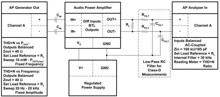
Figure 5 shows an Audio Precision II (AP-II) system setup for measuring the THD+N of
differential-BTL APAs. The bandwidth is usually limited with filters in the analyzer to reduce the out-of-band noise; however, this also reduces relevant harmonics of the higher frequency signals. A filter cutoff frequency of 30 kHz is used for class-AB and class-D APAs to allow measurement of the third harmonic for a 10 kHz signal. The narrow bandwidth attenuates the distortion at higher frequencies, but these harmonics are beyond the audible threshold of the human ear and are not a factor.
Three measurements that express THD+N in some manner in the data sheets are THD+N versus output power, THD+N versus frequency, and the maximum output power bandwidth, covered respectively in the following Sections 4.1 through 4.3. Section 4.4 provides a means to calculate and measure the maximum input voltage for an APA. These measurements vary with CBYPASS for devices that have a BYPASS pin, with THD+N increasing as CBYPASS decreases.
Regulated Power Supply V+ GND Channel A AP Generator Out -+ THD+N vs POUT: Outputs Balanced Zout = 40 Ω
Set Load Reference = RL Sweep 10 mW - POUT(max) Fixed Frequency
Inputs Balanced AC-Coupled Zin = 100 kΩ/185 pF Set Load Reference = RL Internal Filter = 30 kHz Reading Meter = THD+N Ratio Audio Power Amplifier
IN-IN+ OUT+ OUT-VS GND Diff Inputs BTL Outputs THD+N vs Frequency: Outputs Balanced Zout = 40 Ω
Set Load Reference = RL Sweep 20 Hz - 20 kHz Fixed Amplitude Low-Pass RC Filter for Class-D Measurements CIN RL CIN RFILT CFILT
RFILT CFILT Channel A AP Analyzer In
-+
Figure 5. THD+N Measurement Circuit Using the AP-II Measurement System: Differential-BTL
4.1 THD+N vs Output Power
A graph of THD+N versus output power is shown in Figure 6. The signal generator sweeps the input voltage from low to high amplitude at a fixed frequency. The output power is calculated for a given load impedance that is entered into the audio analyzer software. At each voltage step the fundamental frequency is measured first, then filtered out and the amplitude of all the remaining harmonics is measured. This value is then divided by the amplitude of the fundamental frequency and graphed as a percentage of the fundamental.
The higher distortion at low values of POUT is due to the decrease in signal-to-noise ratio as the
harmonics decrease in amplitude below the noise floor (Reference 4). The sudden increase at the upper level of POUT is due to clipping of the output signal.
0.02 2.0 0.2 0.01 0.1 1.0 VS = 3.3 V AV = 12 dB Class-AB RL = 8 Ω AV = 6 dB Class-D CB = 1 µF f = 1 kHz BTL THD+N (%) Class-AB Class-D POUT (W)
4.2 THD+N
vs
Frequency
A graph of THD+N versus frequency is shown in Figure 7. The signal generator sweeps the frequency from 20 kHz to 20 Hz at a fixed voltage. The harmonics and noise of the APA output are measured at specified frequency steps. Each step is divided by the amplitude of the
fundamental frequency and graphed as a percentage of the fundamental. This graph provides a check when compared to the THD+N versus power since they should match at one specific frequency and power.
The increased THD+N at low frequencies is primarily due to the 1/f noise. The high frequency THD+N increase is due to device nonlinearities, primarily crossover distortion, and is expected because the APA open loop gain decreases with frequency. The audio quality is unaffected because the harmonics are above the audible threshold of the human ear (Reference 5). The rolloff at high frequencies is due to the band-limiting filter in the analyzer, which attenuates the upper harmonics above 30 kHz. Setting the filter frequency higher reduces the accuracy of the measurement with D APAs, and will have little or no impact on AB APAs. The class-AB graph continues in a relatively straight line if there is no filter present. The class-D rolls off more than class-AB because of the RC measurement filter, which adds another pole at 30 kHz.
0.02 2.0 0.2 20 200 2k 20k VS = 3.3 V AV = 12 dB Class-AB RL = 8 Ω 6 dB Class-D CB = 1 µF POUT (class-AB) = 250 mW BTL POUT (class-D) = 300 mW THD+N (% ) Class-AB Class-D Frequency (Hz)
Figure 7. THD+N vs Frequency for the TPA2001D1 and the TPA731
4.3 Maximum Output Power Bandwidth
The maximum output power bandwidth is a THD+N versus frequency measurement. The APA is driven at the maximum output power into the load and the frequency is swept from 20 Hz to 20 kHz. The maximum power bandwidth is then specified as the frequency range over which the THD+N remains below a specified percentage, which is normally one percent.
4.4 Maximum
Input
Voltage
The maximum input voltage required for producing maximum output power can be found by increasing the input until the output clips, then reducing it until it is just below clipping. Another method is to calculate the maximum peak-to-peak input voltage using the maximum-rated RMS output power from the data sheet or back-calculate it from the THD+N versus power
measurement at the maximum desired value of distortion. Equation (4) provides the maximum peak-to-peak input voltage, where POUT(max) is the maximum rated RMS output power, RL is the
V L (max) OUT ) P P ( IN A R P 2 2⋅ ⋅ ⋅ = − V (4)
5 Noise
Two types of measurements fall under the noise category, integrated noise over the audio band and signal-to-noise ratio (SNR) of the output signal.
5.1 Integrated Noise vs Frequency
The noise measurement circuit is shown in Figure 8 for an APA with differential inputs and BTL outputs. A graph depicting the output noise voltage of the TPA2001D1 and the TPA731 is shown in Figure 9. All of the inputs of the APA should be ac-coupled to ground through the input
resistor, whether internal or external, to reduce noise pickup and accurately simulate the system. A graph of THD+N versus POUT is shown in Figure 6. The AP generator outputs are not used in
this measurement and should be turned off.
The analyzer should be set to measure amplitude and should be limited to measure the noise in the audio spectrum only. The bandwidth is limited to the range of 22 Hz – 22 kHz with filters in the analyzer. The data field of the sweep panel is set to measure the analyzer amplitude (Anlr Ampl) and the source field is set to sweep the generator frequency (Gen Freq) which is swept from 20 kHz to 20 Hz. The output should be set to V RMS and may be divided by the gain to get the input referred noise voltage, though the data sheets normally specify the output noise voltage in µV RMS. Regulated Power Supply V+ GND Inputs Balanced AC-Coupled Zin = 100 kΩ / 185 pF
Set Load Reference = RL
Internal Filter = 22 Hz - 22 kHz Reading Meter = Amplitude Data1 = Analyzer Amplitude Source = Generator Frequency Audio Power Amplifier
IN-IN+ OUT+ OUT-VS GND Diff Inputs BTL Outputs RC Low-Pass Filter for Class-D Measurements CIN RL CIN RFILT CFILT
RFILT CFILT Channel A
AP Analyzer In -+ Channel A AP Generator Out -+
Outputs Off (No Connect) Sweep 20 kHz - 20 Hz
1 10 100 20 200 2k 20k VS = 3.3 V AV = 12 dB Class-AB RL = 8 Ω AV = 6 dB Class-D CB = 1 µF BTL VOUT ( µ Vrms) Class-AB Class-D Frequency (Hz)
Figure 9. Measured Results of Noise Circuit
5.2 Signal-to-Noise
Ratio
The signal-to-noise ratio (SNR) is the measure of the maximum output voltage compared to the integrated noise floor over the audio bandwidth, expressed in dB. It is normally specified at a precise power in the data sheet tables. The integrated noise floor is measured using the
technique described in Section 5.1. The distortion of the output waveform is then measured at 1 kHz by sweeping the input voltage. The AP setup is the same as per the THD+N versus power measurements, with VOUT, in V RMS, graphed on the x-axis rather than POUT. The point at which
the output voltage begins to clip (the THD+N increases sharply) is considered to be the maximum output voltage.
The SNR is calculated using Equation (5). The noise and signal data can also be expressed in decibel-volts (dBV), which is the dB ratio of the measured voltage to 1 V, and Equation (5) then simplifies to Equation (6). ⋅ = RMS NOISE RMS OUT V V log 20 SNR (5) NOISE OUT dBV dBV SNR= − (6)
Any unused input should be ac-grounded. The measurement bandwidth should be limited to provide an accurate measurement of the integrated noise floor.
6
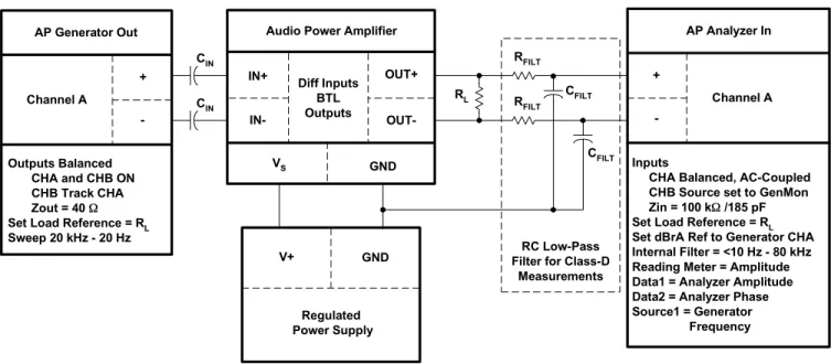
Gain and Phase
The AP measurement circuit is shown in Figure 10 for a mono-channel, BTL-output APA. Measurements for the TPA731 and TPA2001D1 are shown in Figures 11 and 12. The gain and phase can also be measured at multiple points with an oscilloscope using Equation (7) for the gain and Equation (8) for the phase, where ∆t is the time delay between the input and output voltages and f is the frequency of the input signal. The data is then plotted versus frequency.
⋅ = IN OUT V V V log 20 ) dB ( A (7) o 360 f ∆t θ= ⋅ ⋅ (8)
Regulated Power Supply
V+ GND
Inputs
CHA Balanced, AC-Coupled CHB Source set to GenMon
Zin = 100 kΩ /185 pF
Set Load Reference = RL
Set dBrA Ref to Generator CHA Internal Filter = <10 Hz - 80 kHz Reading Meter = Amplitude Data1 = Analyzer Amplitude Data2 = Analyzer Phase Source1 = Generator Frequency Audio Power Amplifier
IN-IN+ OUT+ OUT-VS GND Diff Inputs BTL Outputs RC Low-Pass Filter for Class-D
Measurements CIN RL CIN RFILT CFILT
RFILT CFILT Channel A
AP Analyzer In -+ Channel A AP Generator Out -+ Outputs Balanced CHA and CHB ON CHB Track CHA Zout = 40 Ω
Set Load Reference = RL
Sweep 20 kHz - 20 Hz
Figure 10. Gain and Phase Measurement Circuit
Figure 10 is the AP-II setup for measuring a single channel of the APA. Both channels must be turned on at the generator panel in the software and CHB set to track CHA. The analyzer CHB is set to GenMon (generator monitor), which means it takes its input directly from the generator output of the selected channel internal to the AP-II and uses it as the input phase reference for the analyzer measurement. The reference dBrA value should be set equal to the channel being swept, which in this case is CHA. This sets the input voltage of channel A as the reference for the gain measurement. It may be necessary to subtract 180° from the phase measurement to get the actual phase value.
The APA input ac-coupling capacitors produce the phase shift and attenuation at low frequencies. The class-D RC filter introduces some attenuation and phase shift at the
measurement endpoints as seen in Figure 12. The AP analyzer band-pass filters should be set <10Hz and ≥ 30 kHz to minimize their impact on the measurement.
14 +40 Phase (Degree s) 12 Gain ( dB) 0 VS = 3.3 V AV = 12 dB RL = 8 Ω PO = 250 mW CB = 1 µF BTL 10 Gain Phase -40 8 200 2k 20k 20 n Freque cy (Hz)
+60 24 Phase (D egre e s) Gain (dB) 20 0 Gain Phase VS = 3.3 V AV = 23.5 dB RL = 8 Ω PO = 300 mW CB = 1 µF BTL 16 -40 Frequency (Hz) 20 200 2k 20k
Figure 12. TPA2001D1 Gain and Phase Measurements
7 Crosstalk
Crosstalk is the measure of the signal coupling between channels of a stereo device. The crosstalk measurement circuit is shown in Figure 13 for an APA with differential inputs and BTL outputs. This particular circuit is set up to measure right-to-left (R-L) channel crosstalk, or the amount of signal that couples from the right channel (CHA) into the left channel (CHB). An input signal is fed into the right channel and the outputs of both channels are measured and compared as shown in Equation (9). The input voltage is fixed and is swept from 20 kHz to 20 Hz. The setup is inverted to graph the L-R channel crosstalk and the terms in parentheses in Equation (9) are inverted. ⋅ = OUT CHA OUT CHB V V log 20 Crosstalk (9)
Regulated Power Supply V+ GND Inputs Balanced, AC-Coupled Zin = 100 kΩ/185 pF
Set Load Reference = RL
Set dBrB Ref to CHA
Internal Filter = <10 Hz - 22 kHz Reading Meter = Crosstalk Data1 = Analyzer Crosstalk Source1 = Generator Frequency Audio Power Amplifier
IN-IN+ OUT+ OUT-VS GND Right Channel RC Low-Pass Filter for Class-D Measurements CIN RL CIN Channel A AP Analyzer In -+ Channel A -+ Outputs Balanced CHA and CHB ON CHB Track CHA Zout = 40 Ω
Set Load Reference = RL
Sweep 20 kHz - 20 Hz Channel B -+ IN-IN+ OUT+ OUT-Left Channel CIN CIN RL Channel B -+ AP Generator Out
Figure 13. Crosstalk Measurement Circuit
Both channels must be turned on at the generator panel in the software and CHB set to track CHA. The input is swept over the audio frequency range at constant amplitude. The input voltage should be set to the highest amplitude that does not cause the output voltage to clip. Equation (10) is used for deriving the maximum peak-to-peak input voltage, where POUT(max) is the
maximum rated RMS output power, RL is the load resistance, and AV is the voltage gain of the
APA. The internal filter can be set to 30 kHz or greater to limit noise, but is otherwise not required. The output cables of each channel should be separated to minimize capacitive coupling between them.
V L (max) OUT ) P P ( IN A R P ⋅ ⋅ ⋅ = − 2 2 V (10)
Connections for the measurements of SE devices are made in the same way as for BTL
devices, but with one end of RL tied to ground and a capacitor inserted between RL and OUT+ of
the APA. The measurement is taken across RL only, and not across RL and the capacitor.
A graph of the R-L crosstalk is shown in Figure 14. When both R-L and L-R crosstalk
measurements are shown, the graphs of both channels of the device are different. This is due to impedance mismatch between the channels, which is caused by nonsymmetrical layout of the IC.
The crosstalk was measured for the TPA0212 class-AB APA and TPA2001D2 class-D APA. The values are in close agreement with the data sheet graphs. The class-D crosstalk improves as the supply voltage is decreased because the radiation from the traces is decreased. Class-AB amplifiers are relatively unaffected by changes in supply voltage. The crosstalk increases in all amplifiers as the signal gain increases.
0 Class-AB Class-D VS = 3.3 V AV = 12 dB Class-AB RL = 8 Ω AV = 6 dB Class-D CB = 1 µF POUT = 250 mW Class-AB BTL POUT = 300 mW Class-D Cro sstalk (d B) -60 -120 Frequency (Hz) 20 200 2k 20k
Figure 14. Crosstalk Measurements
8 Supply
Rejection
Two types of supply rejection specifications exist: power supply rejection ratio (PSRR) and supply ripple rejection ratio (kSVR). PSRR is a dc specification measuring the change in output
offset voltage for a change in supply voltage. kSVR is an ac specification measuring the ability of
the APA to reject ac-ripple voltage on the power supply bus. All power supply decoupling capacitors are removed from class-AB circuits, and class-D measurements have a small 0.1µF decoupling capacitor placed close to the APA power pins to provide reverse path for recovery switching currents. It is recommended that the designer use equal decoupling capacitance values when comparing devices from different manufacturers to get a valid comparison of the performance, because a higher capacitance equates to a better kSVR.
PSRR is the ratio of the change in the output voltage, VOUT(dc) for a change in the power supply
voltage, VS, expressed in dB as shown in Equation (11). For example, the output voltage of an
audio power amplifier that has a PSRR of -70 dB would change by 31.6µV if the supply voltage changed by 0.1V. ∆ ∆ = S ) dc ( OUT V V log PSRR 20 (11)
kSVR is the ratio of the output ripple voltage, VOUT(ac), to the supply ripple voltage, expressed in dB
as shown in Equation (12). This parameter is normally listed as a typical value in the data sheet tables at a specified frequency and temperature of 1 kHz and 25°C, respectively. A graph is provided in the data sheet of the typical values of kSVR over the audio bandwidth, because it is a
frequency-dependent parameter. = S ) ac ( OUT SVR V V log k 20 (12)
The PSRR and kSVR measurement circuit is shown in Figure 15. The PSRR measurement
requires only the two DMMs; therefore RSVR, CSVR, the generator and analyzer, and the RC
measurement filter are not needed. The power supply voltage, VS, is initially set, then read from
the meter on the power supply. When the power supply meter does not have the desired
resolution, DMM1 is used to measure VS. DMM2 then measures VOUT across the load. VS is then
stepped up or down by a specific amount and the corresponding value of VOUT is measured.
The differences of the two measurements are then substituted into Equation (11) and the PSRR is calculated for that specific change in supply voltage. PSRR is specified as a typical value that is valid for a given supply voltage range at 25°C. All APA inputs are ac-coupled to ground.
Regulated Power Supply V+ GND Inputs Balanced, AC-Coupled Zin = 100 kΩ/185 pF
Set Load Reference = RL
Internal Filter = <10 Hz - 80 kHz Reading Meter = Crosstalk Data1 = Analyzer Crosstalk Source1 = Generator Frequency Audio Power Amplifier
IN-IN+ OUT+ OUT-VS GND Diff Input BTL Output RC Filter for Filter-Free Class-D Measurements RL Channel B -+ Channel A AP Generator Out -+ Outputs Unbalanced-Float CHA ON CHB Track CHA Zout = 20 Ω
Set Load Reference = RL
Sweep 20 kHz - 20 Hz CIN CIN Channel A -+ CSVR C
The 0.1 µF capacitor, C, is required for class-D operation.
VOUT
(DMM2)
VS
(DMM1)
RSVR
The PSRR measurement uses the DMMs only because it is a dc value. kSVR measurements use either the analyzer, oscilloscope or DMMs because it is an ac value. RSVR and CSVR are used for kSVR measurements only.
AP Analyzer In
Figure 15. PSRR and kSVR Measurement Circuit
The kSVR measurement requires the generator, analyzer, a DMM, and the kSVR filter components
RSVR and CSVR. The RC measurement filter is used when the analyzer cannot accurately process
the square wave output of the filter-free class-D APAs. DMM1 is used to measure VS at the APA
power pins. The generator injects a small sine-wave signal onto the power bus, and the audio analyzer measures this ac voltage at the APA power pin and at the output. Here the AP-II is configured for a crosstalk measurement, and sweeps the ac voltage at constant amplitude over the audio band, measuring and presenting a graph of the data points in dB.
Alternatives to the generator are to use a power source that has the capability to add an ac component to the output, or use a transformer to couple the ac signal onto the power bus. In any case, check the voltage that is applied to the APA power pins to be sure that the absolute
maximum ratings of the APA are not exceeded at any point during the process.
The kSVR filter circuit is shown in Figure 16. The dc power supply output impedance, RS, is
normally in the milli-ohms. The input impedance of the APA power pin, RAPA, is very high
compared to this (in the hundreds or the thousands). The generator output signal sees RAPA and
RS in parallel and, because of the low value of RS, this appears to be an ac ground. The resistor
RSVR is added to the circuit to increase the equivalent impedance of the power supply and is
chosen to be approximately equal to the output impedance of the ac signal generator, RGEN. A
voltage divider, formed between RSVR and RGEN, provides a reasonable amplitude ac signal at
the APA power pin. The large value of RSVR is tolerable because the dc and ac supply currents
are low. This is because the APA is idling and does not have any audio signal at the inputs, so the power dissipated in RSVR is small.
VGEN
RGEN CSVR RSVR
RAPA RS
Figure 16. kSVR Filter Circuit
The addition of CSVR ac-couples the generator to the power bus and provides a high-pass filter
for injecting the ac signal into the APA. The filter cutoff frequency, fC, should be set below the
lowest frequency of the audio band, fMIN, which in this case is 20 Hz. Equation (13) provides the
value for fC, which is ~14 Hz.
2 f
fc = MIN (13)
The equivalent resistance of Figure 20 is then calculated with Equation (14), where RAPA is the
supply voltage divided by the quiescent current of the device (VS/IQ). The value for CSVR is then
calculated using Equation (15).
SVR GEN S SVR APA GEN EQ R R ll(R R ) R R R = + + ≈ + (14) EQ C SVR R f 2 1 ⋅ ⋅ π = C (15)
The capacitor will most likely be electrolytic due to the value required. It will have some reactance that will vary with frequency range as shown by Equation (16). At 20 Hz the impedance will be quite high―approximately the value of RGEN and RSVR―and at 20 kHz the
value will be in the milli-ohms. SVR C C 2 f 1C X SVR ⋅ ⋅ π = (16)
The actual values for the measurement circuit were RGEN = 20Ω, RS = 0, RAPA = 5V/6mA = 833Ω,
CSVR = 330µF, RSVR = 20Ω, fC = 12 Hz. This yields a capacitive reactance of 24 Ω at 20 Hz, and
24 mΩ at 20 kHz. The value of the ac signal may need to be adjusted at low frequencies so that the desired voltage is applied to the APA power pin. The same is true for the dc voltage from the power supply, since IQ will create a small voltage drop across RSVR.
Those devices with BYPASS pins will have improved kSVR as the capacitance on the pin is
increased. Devices operated SE have lower kSVR, particularly at the extreme low and high ranges
of the audio frequency band. This is primarily due to the large output ac coupling capacitor, which dominates the frequency response both below and above the resonant frequency set by the equivalent series resistance (ESR) and equivalent series inductance (ESL) of the capacitor. The kSVR graphs are shown in Figure 17 for a 100-mV RMS input sine wave. Both of these
devices are differential input and BTL output. The TPA731 is measured with the inputs floating, though newer devices are measured with the inputs ac-grounded. Figure 18 is a data sheet graph from the TPA711 that provides an example of how CB impacts the kSVR
measurement of an SE output. 0 -100 Class-AB Class-D VS = 3.3 V AV = 12 dB Class-AB RL = 8 Ω AV = 6 dB Class-D CB = 1 µF BTL KSVR (dB) -60 20 200 2k 20k Frequency (Hz)
Figure 17. kSVR of the TPA2001D1 and TPA731
-50 -60 -80 -100 20 100 1k -30 -20 0 10k 20k -10 -40 -70 -90 BYPASS = 1/2 VD D C B= 0 .1 µ F VD D= 5 V R L = 8 Ω S E C B= 1 µ F kSVR (dB) Frequency (Hz)
9
Power Measurements and Related Calculations
Several sets of data can be extracted from power measurements of a device. The power measurement process begins with the primary measurement of amplifier efficiency. The power that is dissipated by the amplifier is then calculated. This is useful for comparing the power supply requirements of different devices. The crest factor (CF) of the audio signal directly impacts the output power, and the effects are demonstrated from the dissipated power calculations.
9.1 Efficiency
Measurements
Efficiency is the measure of the amount of power that is delivered to a load for a given input power provided by the supply. A class-AB APA acts like a variable resistor network between the power supply and the load, with the output transistors operating in the linear region. They dissipate quite a bit of power because of this mode of operation, and are therefore inefficient. The output stage in class-D APA acts as a switch that has a small resistance when operated in the saturation region, which provides a much higher efficiency.
A circuit for measuring the efficiency of a class-AB or class-D system is shown in Figure 19. The simplest setup results when the power supply voltage and current meters have the resolution required. When the supply current meter is not sufficient, R1 is placed in the circuit. It should be
a small value (0.1Ω) and able to handle the power dissipated. A voltage drop occurs across R1,
so the supply voltage must be adjusted to set the desired VS at the device power pin. The
average voltage, V1, across R1 provides the average supply current (IS = V1/R1) that is used to
calculate the average power provided by the supply.
The true-RMS DMMs and the audio analyzer provide an RMS value of both the voltage and the current, which, when multiplied together, provide the average power. When used, the power supply meters provide the average value of the supply voltage and current. The oscilloscope can measure the average or RMS values of the power supply and output voltage. Some
oscilloscopes even have current probes that can be used to measure the current through a wire, in which case resistor R1 is not needed.
The load measurement is different for class-AB and class-D APAs. Two elements are shown; one is the actual load, ZL, and the other is resistor R2. The Class-AB load is a noninductive
power resistor, ZL = RL, that must capable of handling the maximum power output without a
significant temperature increase, which will change the resistance and impact the measurement accuracy. This purely resistive load makes the output measurement easy since only the voltage across the load, VOUT, is required in order to calculate the output power. The output is sinusoidal
so all measurement devices should be ac-coupled to the load. There is some quiescent power dissipation in RL, but this is negligible. Resistor R2 is not required for class-AB efficiency
The switching nature of the class-D makes the output measurement more challenging. First, a speaker is used as the load for the filter-free class-D because it has the inductance that helps provide the high class-D efficiency. A purely resistive load is not a true indicator of the operating environment of the filter-free class-D, and does not provide accurate efficiency numbers.
Second, the output power must be calculated on the basis of current and voltage, not on the basis of impedance, because impedance varies with frequency. A small power resistor (R2) is
placed in series with the load and a DMM or analyzer is used to measure the RMS value of the load current (IOUT = V2/R2). The RMS voltage across the entire load (speaker and resistor R2)
must be measured to provide the total power into the load. Audio Power Amplifier
IN-IN+ OUT+ OUT-VS GND Diff Input BTL Output R2 V2 (DMM2) RC Filter for Filter-Free Class-D Measurements Inputs Balanced, DC-Coupled Zin = 100 kΩ/185 pF
Set Load Reference = RL
Set dBrB Ref to CHA Channel 1 (A) Oscilloscope or Analyzer -+ Channel 2 (B) -+ Regulated Power Supply V+ GND R1 V1 (DMM1) VS VOUT
Load ZL is a speaker for class-D APAs and is a purely resistive load for class-AB APAs
CIN CIN Channel A AP Generator Out -+ Outputs Balanced Zout = 40 Ω
Set Load Reference = RL
Set Frequency of Signal
ZL
DMM1 and Channel 2 of the AP/oscilloscope (or a third DMM) are used to measure the average power supply
current and voltage when power supply meters are not accurate. If not used, remove resistor R1.
V3
(DMM3)
Figure 19. Efficiency Measurement Circuit for Class-AB and Class-D BTL APAs
Equation (17) provides the efficiency of the class-AB APA, and Equation (18) provides the efficiency of the class-D APA. The input power of both equations, as stated previously, is just the average voltage applied to the power pins of the APA multiplied by the average value of the power supply current. Average value is used for the power supply measurements since the voltage and current have dc and ac components and are typically nonsinusoidal. The output power is also an average value that comes from the multiplication of two RMS terms.
) ( ) ( ) ( 2 ave S ave S L RMS L S OUT AB Class V I Z V P P ⋅ = = − η (17)
) ave ( S ) ave ( S ) RMS ( R ) RMS ( O ) ave ( S ) ave ( S ) RMS ( O ) RMS ( O S OUT D Class V I R V V I V I V P P ⋅ ⋅ = ⋅ ⋅ = = − 2 2 η (18)
The RC measurement filter is used for making filter-free class-D output measurements when the analyzer or DMM cannot accurately process the switching output waveform. The filter resistance must be large enough to minimize current flow through the filter, while the capacitance must be sized to achieve the desired cutoff frequency, which should be just above the audio band. If the filter resistor is not large enough, the filter current must be accounted for in the efficiency equation. The recommended values of RFILT and CFILT are 1 kΩ and 5.6 nF, respectively. This
provides a filter cutoff frequency of ~28 kHz. The filter is only required with class-D APAs and is discussed in more detail in Section 3.
The efficiency was measured with a 3.3-V supply and the results are shown in Table 3 and Figure 20 using the power supply meter and a Fluke 87III DMM measuring the voltage across the load. The DMM, AP analyzer, and TDS 754 oscilloscope measurements for the class-AB data were in close agreement. The class-D DMM and AP data were similar, but the oscilloscope measured 5-10% higher and is due to the averaging of the oscilloscope, which introduced a somewhat large margin of error, particularly at high power output. The DMM reading is more reliable since it filters out the high frequency harmonics of the switching waveform to provide a more stable low-frequency value.
Table 3. Efficiency Data for the TPA731 and TPA2001D1
Vs (Vave) Is (mAave) Ps (mWave) Vout (mVrms) Pout (mWave) Eff (%) Is (mAave) Ps (mWave) Vr (mVrms) Vout (mVrms) Pout (mWave) Eff (%) 3.3 23 75.9 200 5.0 6.6 3 9.9 0.7 58 0.4 4.1 3.3 28 92.4 250 7.8 8.5 4 13.2 1.3 104 1.4 10.2 3.3 40 132.0 354 15.7 11.9 5 16.5 2.3 200 4.6 27.9 3.3 45 148.5 400 20.0 13.5 8 26.4 3.7 335 12.4 47.0 3.3 56 184.8 500 31.3 16.9 10 33.0 4.5 393 17.7 53.6 3.3 67 221.1 600 45.0 20.4 13 42.9 5.1 486 24.8 57.8 3.3 79 260.7 708 62.7 24.0 17 56.1 6.3 594 37.4 66.7 3.3 89 293.7 798 79.6 27.1 22 72.6 7.4 688 50.9 70.1 3.3 111 366.3 998 124.5 34.0 29 95.7 8.8 824 72.5 75.8 3.3 134 442.2 1197 179.1 40.5 39 128.7 10.3 973 100.2 77.9 3.3 156 514.8 1397 244.0 47.4 55 181.5 12.7 1179 149.7 82.5 3.3 158 521.4 1417 251.0 48.1 74 244.2 15.0 1370 205.5 84.2 3.3 - - - - - 107 353.1 18.3 1664 304.5 86.2 3.3 - - - - - 144 475.2 21.2 1932 409.6 86.2
0 10 20 30 40 50 60 70 80 90 100 0 50 100 150 200 250 300 350 400 450 POUT (mW) Efficiency (% ) Class-AB Class-D
Figure 20. Efficiency Graphs of the TPA731 and TPA2001D1
9.2 Power Dissipated vs Power to the Load
The efficiency measurements provide the information required to calculate the amount of power dissipated, PD, in the amplifier. PD provides some insight into the supply currents that are
required. PD is calculated using Equation (19) and the measured values of supply and output
power from Table 3. It is assumed that the power dissipated in the RC filter, used for the filter-free class-D APA measurements, is negligible.
OUT S
D P P
P = − (19)
Figure 21 shows graphs of PD versus the POUT for the TPA731 class-AB and the TPA2001D1
filter-free class-D APAs, calculated from the efficiency data using Equation (19). The data was measured up to the maximum output power, which occurs just prior to clipping, and can easily be discerned from the THD vs Power graph. The designer can choose the percent distortion (level of clipping) that is acceptable for a system and test the device through that power level.
0 50 100 150 200 250 300 0 50 100 150 200 250 300 350 400 450 POUT (mW) Pd (mW) Class-AB Class-D
9.3 Crest Factor and Output Power
The crest factor (CF) is the ratio of the peak output to the average output. It is typically graphed in terms of output power and is expressed in dB. For example, the CF of a sine wave is 3 dB. Sine waves are used in the characterization of APA performance, but do not give a clear idea of what the performance will be with music. The CF of music may vary between 6 dB and 24 dB. The CF directly impacts the amount of heat dissipated in the device. The higher the CF, the lower the heat dissipated and the higher the ambient operating temperature can be. The PD data
of Section 9.2 can be used to determine the CF of the device.
Equation (20) may be used to calculate CF. Since a sine wave was used for the measurements, the CF is 3 dB, and the average output power (POUT(ave) ) is known. The peak output power
(POUT(pk) ) is calculated by manipulating Equation (20) into Equation (21), where POUT(pk) and
POUT(ave) are expressed in watts and CF is expressed in dB.
= ) ave ( OUT ) pk ( OUT P P log ) dB ( CF 10 (20) ( 10) 10CF ) pk ( OUT ) ave ( OUT P P = (21)
For example, the maximum peak output power is 500 mW at for the TPA731. This is calculated using 250 mW as POUT(ave) and a CF of 3 dB for the output sinusoid. The peak will not change
throughout the calculations, as it is the maximum output power possible and is independent of the output waveform. The CF is then increased in 3 dB steps up to 18 dB and the corresponding POUT(ave) is calculated for each step. The PD in the device is measured for each value of POUT(ave)
using the efficiency measurement circuit.
The efficiency data and CF calculations can help the designer approximate the power that must be provided by the power supply. Table 4 shows the values of power for the supply, load, and what is dissipated in the amplifier for various CFs of the TPA731 class-AB APA and the
TPA2001D1 class-D APA. The table was generated from measured data and calculations using Equations (19) through (21).
Figure 22 shows the graph of PS and POUT versus CF from the data of Table 4. The graph allows
easy comparison of the devices, and it is clear that the class-D APA provides more POUT with
less power from the supply than the class-AB APA. The difference between PS and POUT is the
dissipated power, PD.
Table 4. Power vs Crest Factor
POUT (mWave) Crest Factor (dB) Ps (mWave) Pd (mWave) POUT (mWave) Crest Factor (dB) Ps (mWave) Pd (mWave) 251 3 521 270 410 3 475 66 125 6 366 242 206 6 244 39 63 9 261 198 100 9 129 28 31 12 185 154 51 12 73 22 16 15 132 116 25 15 43 18 8 18 92 85 12 18 14 148
0 105 210 315 420 525 3 6 9 12 15 18 Crest Factor (dB) PS (mW) Po (Class-AB) Ps (Class-AB) Po (Class-D) Ps (Class-D)
Figure 22. Supply and Output Power vs CF for the TPA731 and TPA2001D1
10 Measurement
Pitfalls
This section contains a compilation of reminders to help avoid the various common mistakes, or pitfalls, that are made when measuring the APA devices. While they are not all-inclusive, it is the hope of the author that these may offer some insight that will save time and effort spent
troubleshooting the circuit.
10.1 Effects of Improper Interfacing and Grounding
The primary concern is establishing a good connection to the APA. A good connection allows ground current to flow through a low-resistance return path and reduces noise injection into the system through ground loops. Grounding is a critical part of this connection, particularly at the APA inputs. THD+N levels were measured for various generator connections to a TPA2001D2 Class-D APA and are shown in Figure 23. The class-D has differential inputs and BTL outputs. A balanced generator, used with differential inputs, has a maximum deviation of 0.02% THD+N between a grounded and floating source at low power, a difference that is negligible. The balanced generator provided the lowest value of distortion. It is comparable to an unbalanced generator that has a floating source as long as the positive (+) and negative (-) pins of the source are connected to the corresponding pins of the APA. The performance is degraded by 0.2% at lower power, and 0.01% at high power when the negative (-) pin is grounded at the APA. If the generator source is grounded, the performance decreases by over 0.2% across the power spectrum. A balanced source must therefore be used to remove the common-mode noise and minimize offsets from ground currents to provide the most accurate measurement.
2.0 0.2 10m 100m 1 VS = 5 V AV = 6 dB RL = 8 Ω BTL CB= 1 µF THD+N (%) Balanced Unbal-Flt Unbal-Gnd POUT (W)
Figure 23. Effect of Generator Interface on APA Measurements, THD+N vs Power Shown
It may be necessary to tie the ground pin of the power supply or other system device to chassis ground to remove any 60-Hz component, called ac line or 60-Hz hum, from the signal path. This must be done carefully or ground loops will be formed that will increase distortion. References 4 and 6 have more information on grounding and ground loops.
To sum up the APA connections:
• Use a balanced source with differential inputs, unbalanced source with SE inputs.
• Ground the power supply chassis to remove any 60-Hz hum.
• The RC filter, used when measuring filter-free class-D APAs, should always be connected to ground at the APA to allow a path for return currents and to minimize the ground loop area.
• The lead and/or wire lengths of the filter components should be kept as short as possible.
• Power supply-to-APA and APA-to-load cables must be sized to avoid restricting the current flow.
• AC-ground all unused inputs during measurements.
• Check to be sure the source is warmed up and all measurement devices are calibrated.
10.2 THD+N Measurements
• The load resistance must be properly set in the analyzer software for correct output power.
• In the case of high distortion at lower power, check the ground connections, generator output configuration, and that the input and bypass capacitors are correct.
10.3 Noise Measurements
• Limit the measurement to the audio band, because the noise value is integrated over the specified frequency range.
10.4 Gain and Phase Measurements
• Reference the output voltage to the input voltage.
• Subtract 180 degrees from the phase when the phase shift is graphed greater than 180 degrees, which is often a characteristic of the analyzer.
• Adjust the analyzer bandpass filters to less than 10 Hz and greater than 30 kHz to remove their contribution to the phase shift in the audio band.
10.5 Crosstalk Measurements
• The output cables of both channels should be twisted pair wires to minimize ground loops.
• Reversed output connections result in a crosstalk that is measured in positive dB.
• Unused APA inputs should be ac-coupled to ground. Floating inputs decrease crosstalk.
10.6 Supply Rejection Measurements
• A 0.1µF decoupling capacitor is required for class-D operation during these measurements. All other capacitors should be removed. All decoupling capacitors should be removed for class-AB measurements.
• Be sure the output is being compared with the voltage at the power pins of the chip.
• A small resistor (20 Ω) must be in series with the power supply to develop the input voltage.
• As the value of bypass capacitance increases, kSVR improves (decreases).
10.7 Efficiency Measurements
• Measure the supply voltage at the power pins of the chip.
• The filter-free class-D RC measurement filter should have a high resistance for RFILT, with a
value of 1 kΩ recommended. The current through the filter must be considered when the value is smaller than this.
11 References
1. www.audioprecision.com, Audio Precision Website
2. Design Considerations for Class-D Audio Power Amplifiers (SLOA031) 3. Reducing and Eliminating the Class-D Output Filter (SLOA023)
4. Audio Measurement Handbook, Metzler, Bob, Audio Precision, 1993.
5. Introduction to Electroacoustics and Audio Amplifier Design, Leach, W. Marshall Jr., Kendall/Hunt Publishing, 1999
Texas Instruments Incorporated and its subsidiaries (TI) reserve the right to make corrections, modifications, enhancements, improvements, and other changes to its products and services at any time and to discontinue any product or service without notice. Customers should obtain the latest relevant information before placing orders and should verify that such information is current and complete. All products are sold subject to TI’s terms and conditions of sale supplied at the time of order acknowledgment.
TI warrants performance of its hardware products to the specifications applicable at the time of sale in accordance with TI’s standard warranty. Testing and other quality control techniques are used to the extent TI deems necessary to support this warranty. Except where mandated by government requirements, testing of all parameters of each product is not necessarily performed.
TI assumes no liability for applications assistance or customer product design. Customers are responsible for their products and applications using TI components. To minimize the risks associated with customer products and applications, customers should provide adequate design and operating safeguards.
TI does not warrant or represent that any license, either express or implied, is granted under any TI patent right, copyright, mask work right, or other TI intellectual property right relating to any combination, machine, or process in which TI products or services are used. Information published by TI regarding third-party products or services does not constitute a license from TI to use such products or services or a warranty or endorsement thereof. Use of such information may require a license from a third party under the patents or other intellectual property of the third party, or a license from TI under the patents or other intellectual property of TI.
Reproduction of information in TI data books or data sheets is permissible only if reproduction is without alteration and is accompanied by all associated warranties, conditions, limitations, and notices. Reproduction of this information with alteration is an unfair and deceptive business practice. TI is not responsible or liable for such altered documentation.
Resale of TI products or services with statements different from or beyond the parameters stated by TI for that product or service voids all express and any implied warranties for the associated TI product or service and is an unfair and deceptive business practice. TI is not responsible or liable for any such statements.
Following are URLs where you can obtain information on other Texas Instruments products and application solutions:
Products Applications
Amplifiers amplifier.ti.com Audio www.ti.com/audio
Data Converters dataconverter.ti.com Automotive www.ti.com/automotive
DSP dsp.ti.com Broadband www.ti.com/broadband
Interface interface.ti.com Digital Control www.ti.com/digitalcontrol
Logic logic.ti.com Military www.ti.com/military
Power Mgmt power.ti.com Optical Networking www.ti.com/opticalnetwork
Microcontrollers microcontroller.ti.com Security www.ti.com/security
Telephony www.ti.com/telephony
Video & Imaging www.ti.com/video
Wireless www.ti.com/wireless
Mailing Address: Texas Instruments
Post Office Box 655303 Dallas, Texas 75265