Optimized Hardware Implementations of
Lightweight Cryptography
by
Gangqiang Yang
A thesis
presented to the University of Waterloo in fulfillment of the
thesis requirement for the degree of Doctor of Philosophy
in
Electrical and Computer Engineering
Waterloo, Ontario, Canada, 2017
c
I hereby declare that I am the sole author of this thesis. This is a true copy of the thesis, including any required final revisions, as accepted by my examiners.
Abstract
Radio frequency identification (RFID) is a key technology for the Internet of Things era. One important advantage of RFID over barcodes is that line-of-sight is not required between readers and tags. Therefore, it is widely used to perform automatic and unique identification of objects in various applications, such as product tracking, supply chain management, and animal identi-fication. Due to the vulnerabilities of wireless communication between RFID readers and tags, security and privacy issues are significant challenges. The most popular passive RFID proto-col is the Electronic Product Code (EPC) standard. EPC tags have many constraints on power consumption, memory, and computing capability. The field of lightweight cryptography was cre-ated to provide secure, compact, and flexible algorithms and protocols suitable for applications where the traditional cryptographic primitives, such as AES, are impractical. In these lightweight algorithms, tradeoffs are made between security, area/power consumption, and throughput.
In this thesis, we focus on the hardware implementations and optimizations of lightweight cryptography and present theSimeckblock cipher family, theWG-8stream cipher, theWarbler pseudorandom number generator (PRNG), and theWGLCEcryptographic engine.
Simeckis a new family of lightweight block ciphers. Simeck takes advantage of the good components and design ideas of the SIMONand SPECK block ciphers and it has three instances with different block and key sizes. We provide an extensive exploration of different hardware architectures in ASICs and show thatSimeckis smaller than SIMONin terms of area and power
consumption.
For theWG-8stream cipher, we explore four different approaches for theWGtransformation module, where one takes advantage of constant arrays and the other three benefit from the tower field constructions of the finite fieldF28 and also efficient basis conversion matrices. The results in FPGA and ASICs show that the constant arrays based method is the best option. We also propose a hybrid design to improve the throughput with a little additional hardware.
For theWarblerPRNG, we present the first detailed and smallest hardware implementations and optimizations. The results in ASICs show that the area ofWarblerwith throughput of 1 bit per 5 clock cycles (1/5 bpc) is smaller than that of other PRNGs and is in fact smaller than that of most of the lightweight primitives. We also optimize and improve the throughput from 1/5 bpc to 1 bpc with a little additional area and power consumption.
Finally, we propose a cryptographic engineWGLCEfor passive RFID systems. We merge the Warbler PRNG and WG-5 stream cipher together by reusing the finite state machine for both of them. Therefore,WGLCEcan provide data confidentiality and generate pseudorandom numbers. After investigating the design rationales and hardware architectures, our results in ASICs show thatWGLCEmeets the constraints of passive RFID systems.
Acknowledgements
First and foremost, I would like to express my deepest gratitude to my supervisors Professor Mark Aagaard and Professor Guang Gong for their tremendous support, guidance, and encour-agement during the past four and a half years. The continuous help and advice have solved a lot of difficulties I encountered during my research. Their extensive knowledge and expertise in the field have always inspired and motivated me for my research from both the theoretical and practical points of view. Throughout their guidance, I have gained a lot of confidence, which help me think deeply to shorten the gap of the theoretical cryptographic research, hardware im-plementations, and actual applications. Thanks to the positive attitude towards work and life that the professors have provided, the past four and a half years have been an unforgettable time in my entire life that has given me a tremendous development, both academically and personally.
I would also like to express my appreciation to Professor Yunsi Fei From Northeastern U-niversity for serving as my external examiner and giving me many valuable suggestions and comments. I am also grateful to my thesis committee members Professor Anwar Hasan, Profes-sor Hiren Patel, and ProfesProfes-sor Alfred Menezes for their valuable comments and time spent on my thesis, which help to improve the quality of my thesis a lot. This thesis would not have been possible without their guidance and assistance.
I would like to give special thanks to all my colleagues and friends during my PhD studies for their enormous support and valuable discussions. I thank Dr. Xinxin Fan for his help, guidance, and collaboration during the first two years of my study. I thank Dr. Bo Zhu and Dr. Valentin Suder for collaborating on writing a paper with me. I thank Dr. Fei Huo and Nusa Zidaric for helping me polish my English writings. I thank Dr. Kalikinkar Mandal for his help during my last term of studies. Thanks are also given to all the members from the Communication Security (ComSec) lab at University of Waterloo for their support and friendship. They are: Dr. Yin Tan, Kaveh Fazli, Dr. Teng Wu, Shasha Zhu, Yao Chen, Qiao Liu, Bo Yang, Khaled Nassar, Dr. Hayssam EI-Razouk, Ahmed Ayoub, Meng Yang, and many others.
I would like to thank ComSec seminars and the conferences that I have attended (WESS 2013, NIST lightweight workshop 2015, CHES 2015, SAC 2016), which broadened my knowledge and provided me opportunities to exchange ideas with others.
Last but not least, I would like to thank my family for their unconditional and endless love. I am indebted to my parents and my brother for their support, encouragements and sacrifices throughout my life. My deepest gratitude goes to my mother for her endless support and love. None of my work would have been possible without them.
Dedication
To my dearest father
To my loved mother
To my brother
Table of Contents
List of Tables x
List of Figures xii
1 Introduction 1 1.1 Motivation. . . 1 1.2 Thesis Organization . . . 3 1.3 Contributions . . . 4 2 Background 6 2.1 Mathematical Background . . . 6 2.1.1 Finite Field . . . 6
2.1.2 Feedback Shift Register Sequences . . . 8
2.1.3 TheWGTransformation . . . 9
2.2 Symmetric Key Cryptography . . . 10
2.3 Lightweight Cryptography . . . 12
2.3.1 Lightweight Block Ciphers . . . 13
2.3.2 Lightweight Stream Ciphers . . . 17
2.4 Hardware Design and Optimization . . . 22
2.4.1 Hardware Implementations . . . 22
2.4.3 Choice of Bases. . . 25
2.4.4 Tower Field . . . 26
2.5 EPC Passive RFID Systems. . . 26
3 The Simeck Family of Lightweight Block Ciphers 31 3.1 Design Specification and Rationale . . . 32
3.1.1 Specification ofSimeck . . . 32
3.1.2 Design Rationale . . . 35
3.2 Hardware Implementations . . . 36
3.2.1 Metrics and Design Flow . . . 36
3.2.2 Two Different Hardware Architectures forSimeck . . . 37
3.2.3 Hardware Evaluations ofSimeck . . . 42
3.3 Results Comparison betweenSimeckand SIMON . . . 45
3.4 Comparisons with Other Lightweight Block Ciphers . . . 48
3.5 Summary . . . 49
4 Design Space Exploration of the Lightweight Stream CipherWG-8 51 4.1 Description ofWG-8 . . . 52
4.1.1 Parameters forWG-8. . . 52
4.1.2 Overview ofWG-8 . . . 54
4.1.3 Hardware Architecture . . . 55
4.2 Design Strategies for theWG-8Transformation Module . . . 56
4.2.1 Using Constant Array . . . 57
4.2.2 Using Tower Field 1 . . . 57
4.2.3 Using Tower Field 2 . . . 60
4.2.4 Using Tower Field 3 . . . 63
4.2.5 Hybrid Design Architectures forWG-8 . . . 69
4.3.1 Using Finite Field Arithmetic . . . 70
4.3.2 Using Constant Array . . . 71
4.4 Hardware Implementations . . . 71
4.4.1 Finite State Machine . . . 72
4.4.2 FPGA Implementations and Results . . . 72
4.4.3 ASIC Implementations and Results . . . 74
4.5 Results Analysis and Comparison . . . 74
4.5.1 Different Tower Field Methods Analysis. . . 75
4.5.2 Comparisons with Other Lightweight Stream Ciphers . . . 77
4.6 Summary . . . 77
5 WarblerPseudorandom Number Generator 79 5.1 Description ofWarbler . . . 80 5.2 ASIC Architecture . . . 84 5.2.1 Entire Architecture . . . 84 5.2.2 FSM . . . 84 5.2.3 Datapath . . . 86 5.2.4 Throughput Improvement . . . 87 5.3 Results Evaluation . . . 89 5.3.1 ASIC Results . . . 89 5.3.2 Results Analysis . . . 92
5.4 Comparisons with Other Lightweight Primitives . . . 94
5.5 Summary . . . 96
6 WGLCE: A Cryptographic Engine for Passive RFID Systems 98 6.1 WGLCE: Overview . . . 98
6.2 A New Efficient Hardware Implementations of Ultra-lightweight Stream Cipher WG-5 . . . 100
6.2.1 Description ofWG-5 . . . 100
6.2.2 Hardware Architecture ofWG-5 . . . 102
6.2.3 ASIC Results . . . 104
6.3 Design and Implementations ofWGLCE . . . 105
6.3.1 Hardware Architectures . . . 105
6.3.2 Implementation Results and Analysis . . . 107
6.3.3 Interface ofWGLCE . . . 109
6.4 Comparisons . . . 112
6.5 Summary . . . 112
7 Conclusions and Future Work 113 7.1 Conclusions . . . 113
7.2 Future Work . . . 115
List of Tables
2.1 Ten SIMONand SPECKInstances. . . 14
2.2 SIMONand SPECK Parameters . . . 16
3.1 Differences between SIMONandSimeck . . . 36
3.2 The Areas of Basic Gates in the Libraries . . . 37
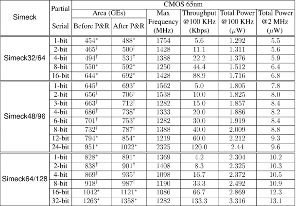
3.3 Our Implementation Results ofSimeck32/64, 48/96, 64/128in 130nm . . . 42
3.4 Our Implementation Results of SIMON32/64, 48/96, 64/128 in 130nm . . . 43
3.5 Our Implementation Results ofSimeck32/64, 48/96, 64/128in 65nm . . . 44
3.6 Our Implementation Results of SIMON32/64, 48/96, 64/128 in 65nm. . . 45
3.7 Breakdown of the Implementation Results for Simeck before the Place and Route in 130nm . . . 47
3.8 Comparisons of Hardware Implementations of Lightweight Block Ciphers . . . . 49
4.1 Tower ConstructionF(24)2 . . . 58
4.2 Exponentiation TableTexp in Hexadecimal Notation . . . 59
4.3 Logarithm TableTlog in Hexadecimal Notation . . . 59
4.4 Tower ConstructionF(24)2 with Normal Bases . . . 62
4.5 Tower ConstructionF((22)2)2 with Normal Bases . . . 64
4.6 Multiplexers and Registers During the Two-clock Computation ofWGP-8(x19) . 68 4.7 The Area, Speed, and Power Consumption Results of FPGA Implementations . . 73
4.9 Area, Speed, and Power Consumption Results for ASIC Implementations in 130nm 76
4.10 The Best Choice of the Tower Field Methods for Different Metrics . . . 76
4.11 The Number of Multipliers and Multiplexers, and the Area of Them in FPGA . . 77
5.1 States Transition Conditions for FSM . . . 86
5.2 Throughput Improvement ofWarbler . . . 88
5.3 Our Implementation Results ofWarblerin CMOS 65nm and CMOS 130nm . . . 91
5.4 The Sequential Logic Ratios ofWarbler . . . 91
5.5 Breakdown of the Implementation Results ofWarblerbefore the Place and Route Phase . . . 93
5.6 The Area Reduction Percentages by using Compile Ultra and Compile Ultra plus Clock Gating . . . 93
5.7 TheWGT1-5andWGT2-5Constant Arrays . . . 94
5.8 Comparisons with Hardware Implementations of Lightweight Primitives . . . 95
6.1 Different Design Options forWGLCE . . . 99
6.2 States Transition Conditions for FSM inWG-5 . . . 103
6.3 ASIC Implementation Results ofWG-5in CMOS 65nm and 130nm . . . 104
6.4 States Transition Conditions for FSM inWGLCE . . . 106
6.5 ASIC Implementation Results ofWGLCEin CMOS 65nm . . . 108
6.6 ASIC Implementation Results ofWGLCEin CMOS 130nm . . . 108
6.7 Breakdown of the Area Results forWGLCEbefore the Place and Route in 130nm108 6.8 The Old Initial Value Pattern for the Internal States ofWarbler . . . 109
6.9 The New Initial Value Pattern for the Internal States ofWarbler . . . 110
6.10 The Location of Keys and IVs . . . 110
List of Figures
2.1 Feedback Shift Register . . . 8
2.2 Block Cipher . . . 10
2.3 Block Cipher Structures. . . 11
2.4 General Structure of a Stream Cipher. . . 11
2.5 Design Tradeoffs between Security, Area, and Throughput . . . 12
2.6 The Round Function of SIMON . . . 14
2.7 The Key Expansion of SIMON . . . 15
2.8 The Round Function of SPECK . . . 16
2.9 SPECKKey Expansion, whereRi is the SPECKRound Function withiacting as the Round Key . . . 17
2.10 TheTriviumStream Cipher . . . 18
2.11 TheGrainStream Cipher . . . 19
2.12 TheWGStream Cipher Family . . . 21
2.13 Hardware Design Process . . . 23
2.14 Reuse the Multiplier in Two Consecutive Clock Cycles. . . 24
2.15 Clock Gating . . . 25
2.16 The Description of an RFID System . . . 27
2.17 The Inventory and Access Protocol between the Reader and the Tag . . . 28
2.18 Threats of an RFID System . . . 29
3.2 The Key Expansion ofSimeck, whereRC⊕(zj)i is theSimeck Round Function
withC⊕(zj)i Acting as the Round Key . . . 34
3.3 Parallel Architecture forSimeck . . . 38
3.4 Fully Serialized Architecture forSimeck . . . 40
3.5 The Top-level I/O Interface between the Cipher and the Outside Environment . . 41
3.6 Comparison of Areas (before the Place and Route) between the Implementation Results of the NSA Researchers’ and Ours in CMOS 130nm . . . 46
4.1 The Initialization Phase of the Stream CipherWG-8 . . . 54
4.2 The Running Phase of the Stream CipherWG-8 . . . 55
4.3 The High-Level Hardware Architecture of the Stream CipherWG-8 . . . 56
4.4 The Hardware Architecture of theWG-8Transformation ModuleWGT-8(x19) . 61 4.5 The Hardware Architecture of Module(·)23−1 . . . 61
4.6 The Integrated Hardware Architecture for ComputingWGP-8(x19)andWGT-8(x19) 68 4.7 The Hybrid Design for the Constant Array based Method . . . 70
5.1 Key/IV Initialization and Running Phases ofWarbler . . . 81
5.2 The Top-level Architecture ofWarbler . . . 85
5.3 Datapath ofWarblerfor Throughput of 1/5 bpc . . . 87
5.4 Datapath ofWarblerfor Throughput of 1 bpc . . . 90
6.1 The Initialization and Running Phases ofWG-5 . . . 101
6.2 The Top Level Hardware Architecture ofWG-5 . . . 102
6.3 The Datapath ofWG-5 . . . 103
6.4 Hardware Architecture with FSM Reuse forWGLCE . . . 106
Chapter 1
Introduction
In recent years, the Internet of Things (IoT) has become pervasive, with many resource con-strained and tiny devices deployed on a large scale and communicating wirelessly with each other and with the Internet at large. Traditional cryptographic primitives, which are designed for desktop computing, do not fit into the constraints of these tiny devices. Therefore, developing security and privacy solutions for these devices and protecting the transmitted and stored data are increasingly important.
1.1
Motivation
Among IoT devices, the Radio Frequency Identification (RFID) system is widely used to perform automatic and unique identification of objects [93]. One important advantage of RFID over barcodes is that line-of-sight is not required. Therefore, it is deployed in various applications, such as product tracking, supply chain management, and animal identification [40]. The growth of RFID has been astounding, and the number of RFID tags is expected to grow to 25 billion by 2020 just for retail apparel and shoes with more tags deployed on high value items [4].
A typical RFID system consists of three components: tags, readers and a back-end database [110, 40, 43]. Each tag is issued with an unique identification number and is attached to an object. Complex tags store information about the object, such as model and serial number, date of production, etc. The readers wirelessly communicate and track these objects via the interrogation process to the tag in order to obtain their data. After that, the readers exchange information about the object with the database through a secure channel. Depending on the power sources of RFID tags, they can be classified into three categories: active, semi-passive, and passive.
Active and semi-passive tags contain batteries. In contrast, passive tags perform computation and communication by using the energy received from the reader’s RF electromagnetic signal. We focus on passive RFID systems in this thesis.
The most popular and widely adopted standard for passive RFID systems is the Electronic Product Code (EPC) Class 1 Generation 2 (EPC C1 G2) standard [2,3], which is also included in the ISO 18000-6 standard. EPC systems operate on the ultra high frequency (UHF) band (860 MHz-960 MHz), the unique identification number is an EPC number, and the read range is around 10 meters. The passive EPC RFID tags are required to be very tiny and inexpensive,i.e., about 5 to 10 cents for each tag, due to large scale deployment [110]. These properties dictate that EPC tags have inherent limited capabilities, such as very limited power consumption, constrained memory and computing capability.
Since the first version of the EPC C1 G2 standard released in 2008 [2], the security and privacy concerns have attracted a lot of attention [104,59,9], because there are no cryptographic mechanisms to protect the tags’ data. Due to the vulnerabilities of wireless communication between readers and tags, the attacker can easily get the EPC number and access the stored data through an unauthorized reader by eavesdropping, leading to unexpected behaviour, such as malicious tracking of the object and modification of tags’ stored data, etc.
Traditional cryptographic primitives which are normally well-suited for desktop computing, such as AES, are often too big and impractical due to the tags’ constrained resources. Moreover, public-key cryptography is infeasible for these applications [77]. In general, the well accept-ed maximum area limit of the security functions for the tags are 2000 GEs (Gate Equivalents) [60, 9, 119, 100], which is around 10% of the total area of an entire tag. However, the small-est available hardware implementation of AES in CMOS 180nm Application Specific Integrated Circuit (ASIC) requires 2400 GEs [82]. In order to overcome this challenge, lightweight cryp-tography is devised to provide secure, compact, and flexible algorithms and protocols that fit into the constraints of resource constrained devices. The term lightweight is used broadly to mean that an algorithm is suitable for use on a constrained platform. In these lightweight algorithm-s, tradeoffs are made between security, area/power consumption, and throughput. Generally, a lower security level than AES is often sufficiently enough, because the amount of encrypted data is tiny during the device’s lifetime [12]. There are currently no well accepted power consump-tion and throughput requirements. The power consumpconsump-tion depends on multiple factors, such as activity factor, clock speed, operating voltage, and the adopted CMOS technology. Thus, it is hard to give an upper bound on the allowed power or energy, but it should be kept as small as possible. The minimum throughput requirement relies on the specific applications.
In recent years, a lot of lightweight algorithms were proposed, such as the stream ciphers Triv-ium[27],Grain[55] and lightweightWG(Welch-Gong) stream ciphers (WG-5[7],WG-7[71],
WG-8[35]); block ciphersTEA[112],XTEA[86],HIGHT[56], SEA[105],PRESENT[17], KATAN and KTANTAN [26], CLEFIA [103], LED [49], PRINCE [18], EPCBC [117], K-LEIN[47], LBlock [113],Piccolo[102], Twine[106], SIMONand SPECK [11] and QTL[68]. In particular, CLEFIA, PRESENT, and Trivium have been adopted by the ISO/IEC Standard 29192. PRESENT-80 andGrain-128 have been adopted by ISO/IEC Standard29167, which provides the cipher suite for the RFID air interfaces. This cipher suite has been specified in the second version of the EPC C1 G2 standard released in 2013 [3], which includes a security exten-sion framework, such as encryption, authentication, etc. Recently, National Institute of Standards and Technology (NIST) began an effort to standardize lightweight cryptography [5].
According to the aforementioned area, power consumption and throughput requirements, the highly optimized hardware implementations of lightweight cryptography are important for con-strained applications. Different cryptographic primitives, such as block ciphers, stream ciphers, and pseudorandom number generators (PRNGs) have different parameters and structures, which affect the hardware implementations and optimizations. Moreover, the hardware performance of the primitive will also influence the parameters and structure selections. As a result, significant emphasis has been given to the hardware implementations in cryptography competition projects, such as stream ciphers in eSTREAM [34], lightweight cryptography in NIST [5], and authenti-cated encryption candidates in CAESAR [20]. To support multiple security needs, implementing multiple cryptography primitives on a constrained device is non-trivial. For example, integrating a PRNG and an encryption algorithm to EPC tags with minimal cost is challenging.
The main research presented in this thesis is to explore efficient low area/power consumption hardware implementations and optimizations of lightweight cryptography, including lightweight stream cipher, lightweight block cipher, lightweight PRNG, and a lightweight cryptographic engine with multiple security functions. With evaluations of the hardware architectures, the impact on selecting appropriate design parameters for a smaller cipher design is also investigated.
1.2
Thesis Organization
The rest of the thesis is organized as follows:
Chapter 2 provides some background and related work. The mathematical background relat-ed to finite field, ferelat-edback shift register sequences, and theWGtransform are firstly reviewed. Then, the related work of lightweight cryptography is provided, and lightweight block ciphers SIMON and SPECK, lightweight stream ciphers Trivium, Grain, and WGare described in
de-tail. We give several efficient hardware implementation techniques, including exploitation of parallelism, clock gating, component reuse and optimizations achieved by choosing appropriate
subfields and different bases representations. Finally, we present the description of the EPC C1 G2 passive RFID system. Additional related work appears in each chapter.
Chapter 3 proposesSimeck, a new family of lightweight block ciphers, which is very suit-able for resource constrained devices. Simeck takes advantage of the good components and design ideas of SIMONand SPECK, and it targets low area/power consumption implementations
while still keeping a reasonable throughput and maximum frequency. We provide an extensive exploration of different hardware architectures in order to make a balance between area, through-put, and power consumption for SIMON and Simeckin both CMOS 65nm and CMOS 130nm
ASICs. We show that it is possible to design a smaller cipher than SIMONin terms of area and power consumption.
Chapter 4 presents the design space exploration of the lightweight stream cipherWG-8for low-cost FPGA and CMOS 65nm and CMOS 130nm ASICs. We explore four different ap-proaches for theWGtransformation module, where one takes advantage of the constant arrays and the other three benefits from the tower constructions of finite fieldF28 and also efficient ba-sis conversion matrices. Many design options have been explored to make trade-offs in terms of area, power consumption as well as throughput. Consequently, the results for FPGA and ASICs are given, and comparisons with other lightweight stream ciphers are provided.
Chapter 5 evaluates hardware implementations and optimizations of Warbler PRNG in C-MOS 65nm and CC-MOS 130nm ASICs. We propose an architecture and a standard interface for the implementations of Warblerwith throughput of 1 bit per 5 clock cycles (1/5 bpc). More importantly, we also improve the throughput from 1/5 bpc to 1 bpc with a little additional area and power consumption. In addition, the LFSR counter-based design is better than the binary counter-based design in terms of smaller area and lower total power consumption. The compar-isons with other PRNGs and lightweight primitives are also given.
Chapter 6 proposes a lightweight cryptographic engineWGLCEfor passive RFID systems. WGLCEis a fusion of theWarblerPRNG and the lightweight stream cipherWG-5, which can be easily integrated into the RFID systems. We investigate the rationale and design choices for WGLCEand explore its different hardware architectures and implementations in CMOS 65nm and CMOS 130nm ASICs. Moreover, we provide an interface for its usage. Finally, we compare our results with other lightweight cyptographic engines.
Chapter 7 concludes this thesis and discusses the future potential research directions.
1.3
Contributions
1. TheSimeckfamily of lightweight block ciphers.
• The smallest block cipher family with key schedule.
• Improved SIMON’s round function by choosing new shift numbers.
• Reduced size ofSimon’s key schedule by choosing a new LFSR polynomial. • First published detailed implementation of fully-serialized Feistel architecture. 2. The lightweightWG-8stream cipher.
• A hybrid design architecture for providing parallelism from 1 bit per clock cycle (bpc) to 11 bits per clock cycle.
• Hardware implementation and analysis of constant arrays and three tower field based methods.
3. The lightweightWarblerPRNG.
• Detailed and smallest hardware implementations ofWarbler.
• Throughput improvement from 1 bit per five clock cycles to 1 bit per clock cycle. 4. The lightweightWGLCEcryptographic engine.
• A cryptographic engine which mergesWG-5andWarblerto provide two function-alities: data confidentiality and generating pseudorandom numbers.
• Hardware implementation analysis of different architectures.
• Loading pattern that simplifies the work of the external environment. 5. Overall lessons.
• Analysis of effects on area and power consumption by use of clock gating and binary vs LFSR counters.
Chapter 2
Background
In this chapter, we first recall some mathematical background in Section2.1. Then, Section2.2
presents the description of symmetric key cryptography. Section2.3reviews a selection of related lightweight symmetric ciphers. In addition, several typical hardware optimization techniques are discussed in Section 2.4. Finally, Section 2.5 describes the system and security issues for a typical passive RFID system.
2.1
Mathematical Background
In this section, we review some mathematical background on finite fields, sequences, and the WGtransformation. For details, the readers are referred to [45,44,52,80].
2.1.1
Finite Field
LetF2 be the finite field with two elements 0 and 1, andF2t be an extension field over the finite fieldF2with2telements, defined by an irreducible polynomial.
A polynomialf(x)is irreducible over F iff(x) is only divisible byc or by cf(x), where c ∈ F. An irreducible polynomial f(x) of degree t over F2 is primitive polynomial if f(x) |
(x2t−1
−1)butf(x)-(xr−1)whenr <2t−1.
Polynomial and Normal Bases
Definition 1 Let α be a defining element ofF2t, which is a root of an irreducible polynomial p(x), i.e., p(α) = 0, where p(x) is an irreducible polynomial of degree t over F2. Then, the polynomial basis of F2t is given by {1, α, α2, · · ·, αt−1}. Thus, any element in F2t can be represented as A =a0+a1α+a2α2+· · ·+at−1αt−1, ai ∈F2.
Definition 2 Let β ∈ F2t, and if the t elements of the set{β, β2, β2 2
,· · · , β2t−1
} are linearly independent overF2t , then we call this set as a normal basis ofF2t overF2. Thus, every element inF2t can be written asA =a0β+a1β2+a2β2 2 +· · ·+at−1β2 t−1 , ai ∈F2. Change of Bases
For every elementA ∈ F2t, it can be represented using any basis. We choose two bases Ψ1 = {α0, α1,· · · , αt−1} and Ψ2 = {β0, β1,· · · , βt−1} of F2t. Assume {ai} ∈ F2 and {bi} ∈ F2 are coordinates of A with respect to Ψ1 and Ψ2 respectively. Let a = (a0, a1,· · · , at−1) and
b= (b0, b1,· · · , bt−1), and assumeΨT2 =C·ΨT1, then,
A = Pt0−1aiαi = a·ΨT1,
= Pt0−1biβi = b·ΨT2 = b·C·ΨT1.
Thus,a=b·C, whereCis defined as the conversion matrix.
Subfield
Definition 3 Let F2n be a finite field with q = 2n elements, andF2n contains a subfield F2m if and only if m is a positive divisor of n. An elementα∈F2n is in the subfieldα∈F2m if and only ifα2m
=α.
Letn = m·k. Then we may consider F2n as an extension field ofF2m. Thus, an element of F2n (i.e., A ∈ F2n) can be expressed as a linear combination of elements in F2m based on a basis withk elements. Assume {γ0, γ1,· · · , γk−1} is a basis of F2n over F2m, then we have A=Pk0−1aiγi, ai ∈F2m.
Trace
Definition 4 Letx∈F2t, and the trace function forxfromF2t toF2 is defined by: T race(x) = x+x2+x22
+· · ·+x2t−1
Theorem 1 The trace function satisfies the following properties.
i. T r(x+y) = T r(x) +T r(y)for allx, y ∈F2t. ii. T r(cx) =cT r(x)for allc∈F2, andx∈F2t. iii. T r(c) =tc(mod2)forc∈F2.
iv. T r(x2i
) = T r(x)2i
=T r(x)for any positivei.
2.1.2
Feedback Shift Register Sequences
Feedback shift registers (FSRs) are common building block for cryptography. A binary sequence {ai}i≥0, ai ∈ F2 can be generated by an n-stage FSR, as shown in Figure2.1. The recursive
a0 a1 a2 an−1an−2 an−3 · · ·
f
Output Sequence · · ·Figure 2.1: Feedback Shift Register relation of the FSR is defined as
an+k =f(ak, ak+1,· · · , an+k−1), k ≥0,
where(a0, a1,· · · , an−1)is aninitial stateand anynconsecutive terms of the sequence represent
a state of the shift register,i.e.,Sk= (ak, ak+1,· · ·, an+k−1)is thek-thstate of the shift register.
The sequence{ai}i≥0is called a linear feedback shift register (LFSR) sequence if the function f is linear,i.e., it is of the form:
f(x0, x1,· · · , xn−1) =c0x0+c1x1+· · ·+cn−1xn−1, ci ∈F2.
Otherwise, it is called a nonlinear feedback shift register (NLFSR) sequence.
The internal state of the FSR can be a non-binary variable, for example, it takes fromF2t, and in this case, a sequence generated by the FSR is a non-binary sequence. In other words, the k-thstate of the FSR is Sk = (ak, ak+1,· · · , an+k−1), ai ∈ F2t. The coefficients of f are also non-binary, i.e.,ci ∈F2t, in order to generate the corresponding feedback for the FSR.
Definition 5 The sequence {ai}i≥0 is called a periodic sequence with period T if ai = ai+T,
i≥0.
Definition 6 Leta={ai}i≥0be a periodic binary sequence with periodT. The autocorrelation function ofa, denoted byCa(τ), is defined as
Ca(τ) = T−1
X
i=0
(−1)ai+τ+ai.
Definition 7 A binary sequence with period 2n−1generated by an n-stage LFSR is called an
m-sequence.
Definition 8 The linear span or linear complexity of a sequence is the length of the shortest LFSR that can generate the entire sequence.
Definition 9 A binary sequence with period2n−1is called a span n sequence if each non-zero
n-tuple occurs exactly once in one period.
2.1.3
The
WG
Transformation
Lett6≡0mod3,3k ≡1modt, andh(x) = x+xq1 +xq2 +xq3 +xq4, whereq
iare given by
q1 = 2k+ 1,
q2 = 22k+ 2k+ 1,
q3 = 22k−2k+ 1,
q4 = 22k+ 2k−1.
Then the functionWGP(·) :F2t →F2t given by
WGP(x) = h(x+ 1) + 1
is called the Welch-Gong (WG) permutation and the functionWGT(·) :F2t →F2 given by WGT(xd) = Tr(WGP(xd))
is known as the Welch-Gong (WG) transformation with decimation d, where d is coprime to 2t−1[46].
2.2
Symmetric Key Cryptography
In symmetric key cryptography, a secret key is shared between the sender and the receiver. Public key cryptography uses two different keys for encryption and decryption. Public key cryptography involves intensive computations, and it is not feasible, at current research stage, for EPC tags due to the area constraint [77]. The security service of confidentiality can be achieved by ciphers, and authentication can be achieved by challenge/response based protocol, where random numbers are used as challenges. In order to meet these requirements, we mainly focus on the block cipher, stream cipher, and pseudorandom number generator in our following work, therefore we give an overview of them.
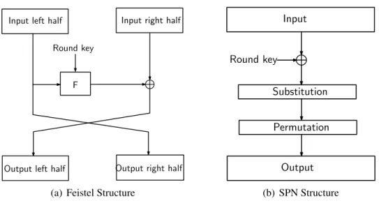
Block cipher: A block cipher encrypts an n-bit block of plaintext with a secret key and outputs an n-bit block of ciphertext at a time. Figure 2.2(a) shows the general structure of a block cipher. In general, the block cipher includes two parts: round function and key schedule, as shown in Figure 2.2(b). The round function is iterated multiple times (called round number), in order to increase the unpredictability between the plaintext and ciphertext [23]. The key schedule is used to provide round keys (ki) for the round function in each round. There are two
common architectures for round functions: the Feistel structure and substitution permutation network (SPN) structure, as shown in Figure2.3. In the Feistel structure, the input message for each round is split into two parts: left half part and right half part. The right half part of the output message directly comes from the input left part and the output left part equals the XORed result of input right half and the output of the functionFwith inputs of round key and input left half. For the SPN structure, each round function includes adding round key, substitution, and permutation layers. The typical cipher of Feistel structure is DES, and that of SPN structure is AES. Block Cipher key xn−1 n n x0 x1 .. . yn−1 y0 y1 .. .
(a) General Structure of a Block Cipher
Round function msgi
Key schedule ki
msgi+1
(b) Round Function and Key Schedule
Figure 2.2: Block Cipher
Stream cipher: A stream cipher encrypts each bit of plaintext individually and the general structure of a stream cipher is given in Figure 2.4. Each bit of the ciphertext is obtained by
L
Input left half Input right half
Output right half Output left half
F Round key
(a) Feistel Structure
Input Substitution L Permutation Output Round key (b) SPN Structure
Figure 2.3: Block Cipher Structures
conducting a bitwise exclusive-or (XOR) operation of each bit of the plaintext and a key bit stream. The key bit stream is implemented by a pseudorandom number generator using a secret key as input [23]. key L Keystream Generator x0x1· · ·xn−1 1 y0y1· · ·yn−1 1 keystream
Figure 2.4: General Structure of a Stream Cipher
Pseudorandom number generator: PRNG is also known as deterministic random number generator, which is constructed from a deterministic function with a secret key, and its output has good statistical properties and approximates a sequence of truly random numbers [89].
2.3
Lightweight Cryptography
The goal of lightweight cryptography is to achieve a balance of the tradeoffs between security, area and throughput. To illustrate it in a block cipher, as depicted in Figure 2.5, the key size
Security Area Through-put Serial Parallel Architecture Short Long Key Size Big Small Round Num ber
Figure 2.5: Design Tradeoffs between Security, Area, and Throughput
provides a tradeoff between security and area, the round number provides a tradeoff between security and throughput, and the implementation architecture provides the area and throughput tradeoff. In general, it is easy to optimize two of them, but it is difficult to consider all of them [93,62,63].
Generally, the proposals of lightweight symmetric ciphers can be divided into three approach-es [93]. The first approach involvapproach-es optimized and compact hardware implementations of stan-dardized algorithms, e.g., compact AES implementations [82, 50, 39, 38]. The second method leverages the slight modification of a well-studied cipher, such as DESXL [94], a lightweight variant of DES. Finally, the third method is to design new ciphers with the goal of having low hardware implementation costs.
Recent proposals include lightweight block ciphers TEA [112], XTEA [86], HIGHT [56], SEA[105],PRESENT[17],KATANandKTANTAN[26],CLEFIA[103],LED[49],PRINCE[18], EPCBC[117],KLEIN[47],LBlock[113], andPiccolo[102],Twine[106], and the more recent SIMONand SPECK[11]. There exist also some lightweight stream ciphers, such asTrivium[27], Grain [55] and lightweight WG (Welch-Gong) stream ciphers (WG-5 [7], WG-7 [71], WG-8 [35]). Additionally, several surveys of recently published lightweight cryptographic imple-mentations can be found in [29,75,66]. In particular, lightweight ciphers have attracted a lot of
attention from industry. CLEFIA, PRESENT, andTriviumhave been adopted by the ISO/IEC Standard29192. PRESENT-80andGrain-128have been adopted by ISO/IEC Standard29167, which provides the cipher suites for the RFID air interfaces.
In this section, we give a review of the lightweight block ciphers SIMONand SPECK which
are related to our cipherSimeck, lightweight stream ciphersTrivium,GrainandWG.
2.3.1
Lightweight Block Ciphers
SIMONand SPECKare two lightweight block cipher families, designed by the NSA’s researchers in 2013 [11,13,12]. Each of SIMONand SPECKcontains ten instances with various block sizes
and key sizes. SIMON and SPECK offer excellent performance on both hardware and software
platforms, such as ASIC, FPGA, and 4/8/16/32-bit microcontrollers, and are designed to perform well across the full spectrum of lightweight applications [11]. SIMONis optimized for hardware
implementations, and SPECKis tuned for optimal performance in software. The round functions
of SIMONand SPECKare based on the Feistel structure.
The following notations are used to describe SIMON, SPECKand ourSimeckin Chapter3.
– x≪candx≫cdenote the cyclic shift ofxto the left and right bycbits respectively. – xyis the bitwise AND ofxandy.
– x⊕yis the exclusive-or (XOR) ofxandy.
– xyis the integer addition modular2nofxandy, wherenis the word size.
The SIMONand SPECK block ciphers withn-bit word size (2n-bit block size), andm-word
(mn-bit) key is denoted as SIMON2n/mnand SPECK2n/mn. There are ten instances for each of
SIMONand SPECK family for the combination ofn andm, wheren ∈ {16,24,32,48,64}and m∈ {2,3,4}. The details of them are listed in Table2.1.
In this thesis, we only consider SIMON2n/mnand SPECK2n/mnwith word sizenequals16, 24, and32, the key wordsmequals4here, in order to be consistent with ourSimeckin Chap-ter3. They are SIMON32/64, SIMON48/96, SIMON64/128 and SPECK32/64, SPECK48/96,
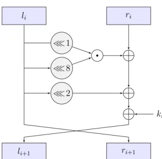
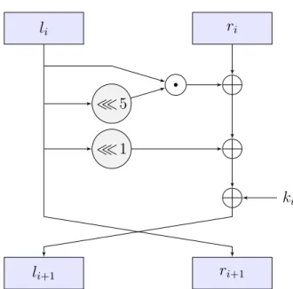
Table 2.1: Ten SIMONand SPECKInstances SIMON SPECK SIMON32/64 SPECK32/64 SIMON48/72 SPECK48/72 SIMON48/96 SPECK48/96 SIMON64/96 SPECK64/96 SIMON64/128 SPECK64/128 SIMON96/96 SPECK96/96 SIMON96/144 SPECK96/144 SIMON128/128 SPECK128/128 SIMON128/192 SPECK128/192 SIMON128/256 SPECK128/256 li ri ki li+1 ri+1 ≪1 ≪8 ≪2
SIMON
Thei-thround function of SIMON(as shown in Figure2.6) is a two-stage Feistel mapRki which is defined by
(li+1, ri+1) =Rki(li, ri) = (ri⊕f(li)⊕ki, li),
wheref(li) = ((li ≪1)(li ≪8))⊕(li ≪2),kiis the round key, and (li,ri), (li+1,ri+1) are
two internal words in thei-thand(i+1)-throunds respectively.li andriare the left part and right
part of the internal words respectively.kiis generated from the key schedule and0≤i≤T −1,
whereT is the number of rounds. The number of rounds for different SIMONinstances are given in Table2.2.
The key schedule (expansion) of SIMON is depicted in Figure2.7. The round keys for the first four rounds (k0, k1, k2, k3) are the four key words,i.e., the input key, of the key schedule,
which is used to generate other round keys. The other round keys are generated by ki+4 =C⊕(zj)i⊕ki⊕[ki+3 ≫3⊕ki+1]⊕[(ki+3 ≫3⊕ki+1)≫1],
where 0 ≤ i < T − 4. The constant C equals 2n −4 = 0xf f· · ·f c. The version
depen-dent constant sequence zj is listed in Table 2.2. z0 = 1111101000100101011000011100110,
a period31 sequence generated by the primitive polynomial X5 +X4 +X2 +X + 1. z 1 =
1000111011111001001100001011010, a period31sequence generated by the primitive polyno-mialX5+X3+X2+X+1. z
2 = 1101101110101100011001011110000001001000101001110011
0100001111, a period 62sequence formed by bitwise XOR of the period 2sequence(01)with z1. In addition,(zj)i is thei-thbit ofzj.
ki+3 ki+2 ki+1 ki
C⊕(zj)i ≫3
≫1
Table 2.2: SIMONand SPECKParameters
block key word SIMON SPECK
size size size constant rounds rotation rotation rounds
2n 4n n sequencezj T α β T 32 64 16 z0 32 7 2 22 48 96 24 z1 36 8 3 23 64 128 32 z2 44 8 3 27 SPECK li ri li+1 ri+1 ki ≫α ≪β
Figure 2.8: The Round Function of SPECK
Thei-thround function of SPECK,shown in Figure2.8, is defined by
(li+1, ri+1) =Rki(li, ri) = ((li ≫αri)⊕ki, ri ≪β⊕(li ≫αri)⊕ki),
where0≤ i≤T −1. The number of roundsT and the rotationsαandβ are different for each instance and they are listed in Table2.2.
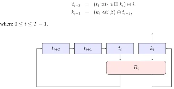
The key schedule reuses the round function to generate the round keyki, as shown in
wherek0 is the first round key. The other round keys are generated by ti+3 = (ti ≫αki)⊕i, ki+1 = (ki ≪β)⊕ti+3, where0≤i≤T −1. ti+2 ti+1 ti ki Ri
Figure 2.9: SPECKKey Expansion, whereRi is the SPECK Round Function withiacting as the
Round Key
2.3.2
Lightweight Stream Ciphers
In this subsection, we present three hardware-oriented lightweight stream ciphers (Trivium, Gain, and WG), where Trivium and Gain are the top finalist of eSTREAM [34] project, and the originalWGparameter are also in the phase 2 of eSTREAM [34] project.
Trivium
Trivium [24, 25] was designed in 2005 to be compact in constrained environments. It can gen-erate up to264 bits of keystream from an 80 bits key (k
0,· · · , k79)and an 80 bits initialization
vector (IV0,· · · , IV79). The cipher itself consists of three NLFSRs (93-bit NLFSR1, 84-bit
NLFSR2, 111-bit NLFSR3), and they are denoted as {a0, a1,· · · , a92}, {b0, b1,· · · , b83}, and
{c0, c1,· · ·, c110}respectively. The feedback of one NLFSR is generated by the output of
an-other NLFSR, as shown in Figure2.10. The process ofTriviumcontains initialization phase and keystream generation phase. More specifically, the 288-bit states of NLFSRs are first initialized
with the key and IV as follows.
(a0, a1,· · · , a92) = (0,· · · ,0, k79,· · · , k0),
(b0, b1,· · · , b83) = (0,· · · ,0, IV79,· · · , IV0),
(c0, c1,· · · , c110) = (1,1,1,0,· · ·,0).
Then, the states are rotated for4×288times based on the following update function. ai+93 = ci+ci+45+ci+1ci+2+ai+24,
bi+84 = ai+ai+27+ai+1ai+2+bi+6,
ci+111 = bi+bi+15+bi+1bi+2+ci+24.
After that, assume the values in the NLSFRs are the starting point of the key generation phase, an output keystream, denoted bys={si}i≥0, can be generated by
si = ai+ai+27+bi+bi+15+ci+ci+45.
The output sequence does not possess any determined randomness properties [23].
a0 a1 a24 a92 · · · a27 · · · a2 b0 b1 b6 b83 · · · b15 · · · b2 c0 c1 c24 c110 · · · c45 · · · c2 N L L L N L L L N L L L L si keystream
Figure 2.10: TheTriviumStream Cipher
Grain
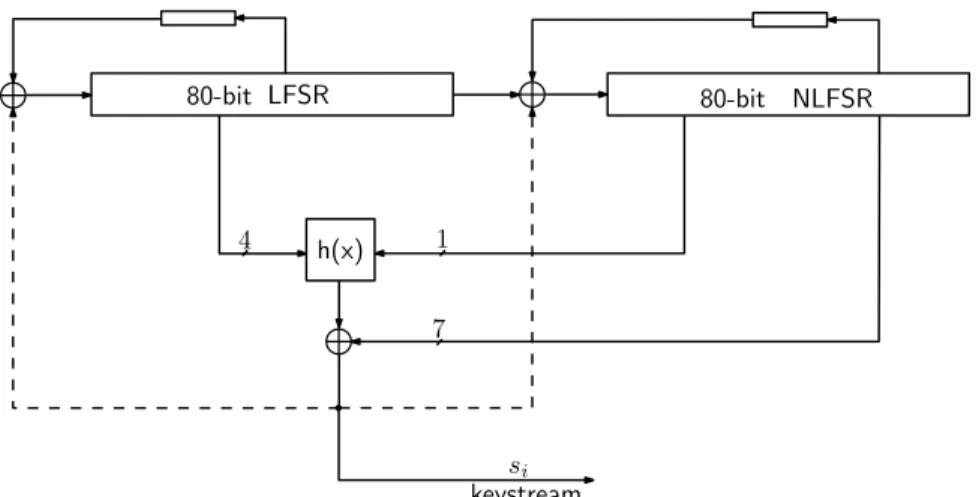
Grain[54, 55, 53] is a lightweight stream cipher designed in 2005 for applications which have very limited hardware resources. The first version of Grainuses an 80 bits key and a 64 bits
IV [54], and the second version supports key size of 128 bits and IV size of 96 bits [53]. This subsection specifies the details of the first version. Grainconsists of three main building parts, a pair of linked 80 bits shift registers and a non-linear filter function. One of the two 80 bits shift registers is LFSR and another one is NLFSR, which are denoted as{a0, a1,· · · , a79}and
{b0, b1,· · · , b79} respectively. In particular, the feedback function of the NLFSR is masked by
the output of the LFSR. The nonlinear filter function is used to introduce nonlinearity to the cipher. Moreover,Grainhas a lower bound of periods of output sequences [23].
Before the keystream generation phase, the cipher must be initialized with the key (ki, 0 ≤
i ≤ 79) and IV (IVi, 0 ≤ i ≤ 63). During this phase, the NLFSR is loaded with the key bits,
where bi = ki, and the first 64 bits of LFSR are loaded with IV, asai = IVi,0 ≤ i ≤ 63. The
remaining bits of the LFSR are filled with ones, i.e., ai = 1,64 ≤ i ≤ 79. Then the cipher is
clocked for 160 times without producing any keystream, which is called the initialization phase. After that, the running phase starts, the output keystream si is generated clock cycle by clock
cycle. The description of them are shown in Figure2.11.
80-bit LFSR L 80-bit NLFSR L h(x) L 4 1 7 si keystream
Figure 2.11: TheGrainStream Cipher
In the initialization phase, the feedback update functions of LFSR and NLFSR are XORed with the output keystream si (as shown in the dashed lines of Figure 2.11). Therefore, the
feedback function of the LFSR is
and the feedback function of the NLFSR is bi+80 = si+ai+bi+62+bi+60+bi+52+bi+45+bi+37+bi+33+bi+28+bi+21+ bi+14+bi+9+bi+bi+63bi+60+bi+37bi+33+bi+15bi+9+ bi+60bi+52bi+45+bi+33bi+28bi+21+bi+63bi+45bi+28bi+9+ bi+60bi+52bi+37bi+33+bi+63bi+60bi+21bi+15+ bi+63bi+60bi+52bi+45bi+37+bi+33bi+28bi+21bi+15bi+9+ bi+52bi+45bi+37bi+33bi+28bi+21, where0≤i≤159.
The output sequencesi is filtered by a non-linear functionh(x). The filtering functionh(x)
is defined as:
h(x) = x1+x4+x0x3+x2x3 +x3x4+x0x1x2+x0x2x3+x0x2x4+x1x2x4+x2x3x4,
wherex0, x1, x2, x3, x4 correspond to the tap positionsai+3, ai+25, ai+46, ai+64, andbi+63
respec-tively. The output keystream, denoted bys={si}i≥0, is defined as:
si =h(ai+3, ai+25, ai+46, ai+64, bi+63) +bi+1+bi+2+bi+4+bi+10+bi+31+bi+43+bi+56.
In the running phase, the feedback function of LFSR is ai+80=ai+62+ai+51+ai+38+ai+23+ai+13+ai,i≥160,
and the feedback function of the NLFSR is
bi+80 = ai+bi+62+bi+60+bi+52+bi+45+bi+37+bi+33+bi+28+bi+21+ bi+14+bi+9+bi+bi+63bi+60+bi+37bi+33+bi+15bi+9+ bi+60bi+52bi+45+bi+33bi+28bi+21+bi+63bi+45bi+28bi+9+ bi+60bi+52bi+37bi+33+bi+63bi+60bi+21bi+15+ bi+63bi+60bi+52bi+45bi+37+bi+33bi+28bi+21bi+15bi+9+ bi+52bi+45bi+37bi+33bi+28bi+21,
wherei≥160. Accordingly, the keystreams={si}i≥160is outputed as shown in the solid lines
of Figure2.11.
WG
TheWG stream cipher family is hardware-oriented stream ciphers based on the WG transfor-mation. It was firstly proposed in 2005 [84] and a complete version was published in 2008 [85].
The structure of theWG stream cipher family is described in Figure2.12. The WGstream ci-pher is composed of a length lLFSR, followed by aWGtransformation with decimationdover
F2m. The optimal decimation parameters which can achieve the highest security level for each WG instance are investigated in [74]. The WG transformation module can be split into WG permutation module and trace module. The characteristic polynomial of the LFSR is a primitive polynomialf(x)of degreeloverF2m, i.e.,f(x) =xl+Pl−1
0 cixi, ci ∈ F2m. TheWG transfor-mation with decitransfor-mationdis described in Section2.1.3, and it exists only whenm6= 0 (mod3). Thus, theWGstream cipher family is defined whenm6= 0 (mod3)overF2m. We denote each specific instance in the family as WG-m stream cipher. Several instances of them have been explored in hardware, such as WG-29[30], WG-16 [36, 37, 31], WG-7[67], and WG-5 [7]. The lightweightWGstream ciphers,WG-5[7],WG-7[71], andWG-8[35] have been proposed for the resource constrained environments. Their security has been analyzed [87,99,74] and can be used in protecting communication in these applications, such as ensuring data confidentiality and performing entity authentication [71].
L L L a0 a1 al−2 al−1 L · · · · · · · · · WGP(xd) WGT(xd) Tr(·) c0 c1 cl−2 cl−1 m m m m m m m m m m m 1 INIT Keystream
Figure 2.12: TheWGStream Cipher Family
TheWGstream cipher contains two phases, the initialization phase and the running phase as shown in the dashed line of Figure2.12. It is executed2lclock cycles in the initialization phase with the recursive values fromWGP(xd) and feedback value of the LFSR. After the initialization
phase, the running phase starts and output the one bit keystream generated by the trace function clock cycle by clock cycle with the recursive value from LFSR only. We define the internal
states of the LFSR overF2m by {ak}k≥0 and the output keystream over F2 by{sk}k≥0. Then, the mathematical expressions for updating the LFSR internal states and generating the output keystream sequence ofWG-mare given by:
ak+l= Pl−1 i=0ciai+k+WGP(adk+l−1) 0≤k <2l, Pl−1 i=0ciai+k k ≥2l. sk=WGT(adk+3l), k≥0.
Theorem 2 The keystream sequence of theWG-mstream cipher has the following properties. i. Period is2n−1, wheren =ml.
ii. It is balanced, i.e., the number of 0’s is only one less than the number of 1’s in one period of the keystream.
iii. It has an ideal 2-level autocorrelation property.
iv. Any t-tuple is equally likely distributed (ideal t-tuple distribution) for1≤t ≤l.
v. The linear span or linear complexity of the keystream can be determined exactly, and in-creased exponentially with m.
2.4
Hardware Design and Optimization
In this section, we discuss hardware implementation technologies and several efficient approach-es for cryptographic primitivapproach-es.
2.4.1
Hardware Implementations
Application specific integrated circuits (ASICs) and field programmable gate arrays (FPGAs) are typical hardware implementation techniques. ASIC is much cheaper than FPGA when the quantity of items is large, while FPGA provides more flexibility. Due to the massive deployment of passive RFID tags, the ASIC implementation of cryptographic primitive is more critical. Our
optimizations and benchmarking emphasize ASICs more than FPGAs. We use CMOS 130n-m and CMOS 65n130n-m for our i130n-mple130n-mentations because EPC tags use older processes with the consideration of cost and compatibility with analog components.
A typical hardware design process is described in Figure 2.13. Firstly, we write our ideas and specification into Register Transfer Level (RTL) code. Then, we synthesis a RTL code to gate level netlist using logic synthesis tool. We use physical synthesis tool to map the gate level netlist to the actual hardware resources in ASIC or FPGA. Finally, the area, power consumption, and clock speed are generated after the physical implementation.
RTL Code Logic Synthesis Physical Synthesis (VHDL, Verilog) Gate-level Netlist Implementation File
Figure 2.13: Hardware Design Process
The total power consumption is a combination of static and dynamic power consumption, i.e.,
Ptotal =PStatic+PDynamic.
The static power consumption is caused by leakage currents inside transistors. The dynamic pow-er consumption is caused by switching activity by charging and discharging of load capacitance Cload, and short circuit currents when transistors switch [58]. However, the switching power
consumption dominates the dynamic power consumption, thus the dynamic power consumption is approximately defined as
PDynamic=α·Cload·fCLK ·V2,
where,αis the switching activity, defined as the number of signal transitions in a clock period. fCLK is the operating clock frequency and V is the supply voltage. For ASIC designs, the
power consumption correlates to the entire FPGA device and the dynamic power consumption correlates to the used area for a specific design [58].
2.4.2
Reuse, Parallelism and Clock Gating
To get an efficient design in hardware, we can use a number of techniques to optimize the design, such as, reuse of a component, parallelism, and clock gating [97,67, 82, 98]. Reuse means that we can reuse the existing modules (combinational modules or registers) in different clock cycles in order to decrease the total area. An example of reuse technique over two clock cycles is shown in Figure2.14. 8
M
8M
8M
a b c e d a c b d e sel sel 1 2Figure 2.14: Reuse the Multiplier in Two Consecutive Clock Cycles.
Parallelism means that we can improve throughput by adding some extra logic but with s-maller area than using several identical designs. These techniques are popular in hardware design which are used to optimize the designs for achieving better results in terms of area, clock speed, and throughput.
Clock gating is a technique for reducing dynamic power consumption and area. For reducing dynamic power consumption, the clock gating reduces the activity factor by turning off the clock when the circuit is not needed. For reducing area, clock gating can replacenregisters with chip-enable with n registers without chip-enable and a clock gating cell, as shown in Figure 2.15. The area of a register with chip-enable is larger than that of a register without chip-enable, as a result the total area is decreased. In our implementation, the power consumption results are
d
en
clk
q
Reg
(a) A Register with chip-enable
d
en
clk
q
Reg
Latch
Clock gating cell
(b) A Register with Clock Gating Cell
Figure 2.15: Clock Gating
conventionally got by letting the primitives continuous run with stopping. Clock gating is part of the circuit and it is for the cryptographic benchmarking purpose.
2.4.3
Choice of Bases
The design of many cryptosystems involve finite field arithmetic operations. Arithmetic addition can be performed using bit-wise XOR operation under the binary representation, but multipli-cation operation is complex and time consuming. The complexity is based on the selection of irreducible polynomial forF2m and the basis used to represent the finite field elements. During the past years, a lot of research have been given to efficient implementations of arithmetic com-putations in finite field [69]. In addition, the hardware cost of the ciphers is related to the basis selected for performing computation inF2m [23].
Polynomial basis is very good for exploring hardware optimization of multiplication oper-ation, because the multiplication operation using polynomial basis can be implemented using simple shift and XOR operations [28]. Normal basis is efficient and cost effective for hardware implementation of squaring. It is simply a cyclic shift of coordinates of the element [61]. Howev-er, the multiplication operation in normal basis is more complex in terms of hardware resources. Optimal normal basis (ONB) [41] is proposed to deal with the constraints in normal basis, which allows not only fast squarings but also fast multiplications with less XOR and AND gates. There are two types of optimal normal bases inF2m, i.e., type-I and type-II, defined as follows:
1) Type-I:m+ 1 is a primep, and 2 is primitive modulop. 2) Type-II:2m+ 1 is a primepand either
i. 2 is primitive modulop, or
However, most ofF2m do not have a type-I ONB, such as odd primem. Thus, type-II ONB gives more advantages when mis odd prime [109]. In conclusion, we need to make a trade-off by choosing an irreducible polynomial for the finite field and by carefully selecting a basis in order to achieve the best performance for the entire design.
2.4.4
Tower Field
A wide variety of efficient hardware implementations of AES has been proposed during the past years. Among them, the best method for achieving a very compact S-box is to use subfield [96, 101,21,108]. Rijmen [96] suggested using subfield arithmetics in the crucial step of computing an inverse in F28 by reducing an 8-bit calculation to several 4-bit ones. Satoh et al. [101] further extended this idea, using the tower field approach of Paar [88], by breaking up 4-bit calculations into 2-bit ones, which resulted in a smaller AES circuit. A number of different tower field constructions for S-box had been explored by Canright in [21], and the smallest one is to use three level tower constructions with normal basis in each level. Recently, Ueno et al. [108] introduced using PRR (Polynomial Ring Representation), RRB (Redundantly Represented Basis) in the tower field constructions for the inversion circuit in S-box. This method leads to a smaller area of the inversion circuit than Canright’s and the corresponding area and time product of S-box is also smaller than that of Canright. Therefore, from the observations of AES, the tower constructions could be useful for efficient implementations of other ciphers.
2.5
EPC Passive RFID Systems
EPCglobal Inc.[2] promotes and leads the standardization of RFID systems, especially for RFID systems operating at 860 MHz - 930 MHz. The Electronic Product Code (EPC) provides iden-tification of items for companies worldwide by storing the EPC number in the so-called EPC memory inside the tags. The EPC Class 1 Generation 2 (EPC C1 G2) UHF (Ultra High Frequen-cy) RFID standard [2,3] is the most popular one for passive RFID systems. In this section, we give an overview of this type of RFID system.
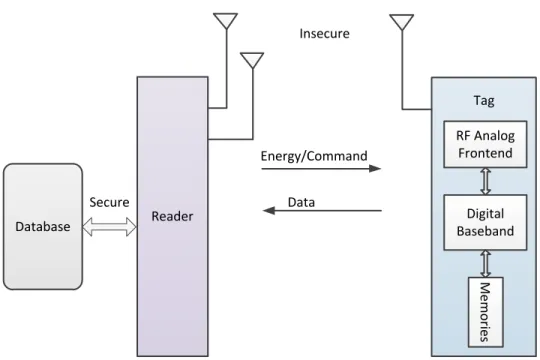
A typical RFID system consists of three entities: a database, a reader, and a tag. In the current EPC C1 G2 standard [2, 3], there is a tag selection phase for the scenario where the reader communicates with multiple tags. After that, the reader has selected one tag. Therefore, we only consider the situation where one reader communicates with one tag. The diagram of an RFID system is shown in Figure2.16. We assume that the back-end database and the reader are
Tag Digital Baseband Reader Database RF Analog Frontend M em o rie s Energy/Command Data Tag Secure Insecure
Figure 2.16: The Description of an RFID System
connected with a secure channel via communication protocols such as SSL/TLS. The wireless communication channel between the reader and the tag is insecure.
The reader initiates all the communication between the reader and tag, and it follows a com-mand/response pattern, where the reader sends a command and the tag responds. As shown in Figure2.16, each tag contains an RF analog frontend, a digital baseband, and four memories. The RF part is used to perform two-way communication with the reader and harvest energy from the reader’s signal. The digital baseband is used to process all the commands and data. The four memories are EPC memory, TID (Tag Identification) memory, Reserved memory, and User memory. The EPC number is used for unique identification, and it is stored in the EPC memory. The TID memory stores the unique tag identification number set by the manufacturer. The kill and access passwords are stored in the Reserved memory. The extra item information, such as the weight, place of origin, and so forth, are stored in the optional User memory. The readers’ database contains the EPC numbers and the associated passwords of all tags.
According to the EPC C1 G2 standard, the inventory and access protocol between the reader and the tag is shown in Figure2.17. In which, the reader has two states: inventory and access. The tag has five states: ready, reply, acknowledged, open, and secure. More specifically, the inventory and access protocol is executed as follows. The reader sends a Query command to the tag, and the tag replies with a 16-bit random number, denoted as RN16 Init. After the reader
Inventory Ready/ Arbitrate Reply Acknowledged Secure Access
Reader
Tag
Query RN16_Init ACK || RN16_Init PC||EPC Req_RN||RN16_Init RN16_Handle Command Execution OpenFigure 2.17: The Inventory and Access Protocol between the Reader and the Tag
receives the RN16 Init, it sends an ACK command with the same RN16 Init to the tag. Then the tag sends the EPC number and PC code to the reader if the RN16 Init it received is correct. PC code is the protocol control bits. Upon receiving it, the reader sends a Req RN command with the RN16 Init to the tag, the tag will reply with a RN16 Handle to the reader after checking the correctness of RN16 Init. The RN16 Handle is another 16-bit random number. After the reader receives the RN16 Handle, the reader may request the tag to execute a command.
Command execution is a multi-round process of bi-directional communication between the reader and tag. The command here can be an access command or a kill command, where the access command transfers the tag from the open state to the secure state, and the kill command transfers the tag from the open state to the killed state. The kill command will disable the tag forever, and the tag cannot respond to the reader any more. However, after the reader successfully sends an access command to the tag which means that the 32-bit access password is correct, the tag will send the same RN16 Handle back and ends up in the secure state. Note that the RN16 Handle is used in the entire procedure of the access command. Then, the reader can send read, write, etc., commands to the tag and the tag will only execute them when it is in the secure state. The exchanged message between the reader and the tag, such as EPC number, RN16 and so on, are very short, and they are typically below 100 bits. Furthermore, RN16 is used for providing verification of the reader identity, and provide cover-code (mask) for the data in access, kill, and write commands.
It is worth mentioning that the two 32-bit passwords for the access and kill commands are designed to be two security features in the first version of the EPC C1 G2 standard [2]. However, the research [111, 40, 43, 51, 22] shows that the two 32-bit passwords can be broken easily if the attacker has the ability to eavesdrop on the bi-directional communications between the reader and the tag. As a result, some optional security requirements are provided in the second version of the EPC C1 G2 standard [3], which was released in 2013. For example, some of these optional security requirements include Authenticate and SecureComm commands. The Authenticatecommand allows the RFID system to perform reader, tag or mutual authentication. TheSecureCommcommand allows encrypted communication between the reader and the tag.
Since the link between the reader and tag is a wireless channel, all the existing attacks on the wireless link also apply to the link between the reader and tag [23]. Moreover, the resource constrained properties of the tag and insecure channel between the reader and tag lead to many vulnerabilities [59, 111, 95]. A diagram about threats on passive RFID systems is depicted in Figure2.18. It describes the authorized and unauthorized entities, including an authorized
read-Unauthorized reader Authorized reader Eavesdropping Insecure Side cha nnel Unauthorized Tag Authorized tag
Figure 2.18: Threats of an RFID System
er, an unauthorized reader, an authorized tag, and an unauthorized tag. Figure2.18also shows the interactions of the entities in the security model. An unauthorized reader can interrogate an authorized tag, and the unauthorized tag can impersonate an authorized one. The unauthorized reader and unauthorized tag can eavesdrop on the insecure wireless channel between the autho-rized reader and authoautho-rized tag. The unauthoautho-rized reader can observe the external information emitted from the authorized tag through the side channel.
Consequently, the attacker can take advantage of the capabilities of the unauthorized reader and unauthorized tag to launch many attacks [42, 90, 81, 95], such as unauthorized tag reading attack, tag data modification attack, man-in-the-middle attack, eavesdropping attack and side
channel attack. These attacks may lead to information disclosure and cause the system to respond in an unexpected or damaging way.
The typical security solution for the attacks is to adopt cryptography to the passive RFID sys-tem, which can provide confidentiality, integrity check, and authentication. Due to the resource constrained properties of the passive RFID tag, lightweight cryptography is devised to solve this problem. Therefore, exploring the hardware performance and optimizations of lightweight cryptography is increasingly important in the IoT era.
Chapter 3
The Simeck Family of Lightweight Block
Ciphers
The security of the recently proposed lightweight block ciphers, SIMON and SPECK [11], have been investigated [15, 8, 19] by the research community since they were public. These ciphers are recognized to be the smallest block ciphers in each of the block/key size categories when used in resource-constrained environments. SIMONis optimized for hardware implementation, while SPECK is optimized for software. Inspired by the designs of SIMON and SPECK, we combine their good components in order to get a new block cipher family, calledSimeckWe use a slightly modified version of SIMON’s round function, and reuse it in the key schedule like SPECK does. Moreover, we take the benefits of using Linear Feedback Shift Register (LFSR) based constants in the key schedule in order to further reduce hardware implementation footprints. The new family of lightweight block ciphers Simeck aims to have comparable security levels but more efficient hardware implementations.
Based on the aforementioned motivations, we have the detailed design goals as follows. Hardware. First, we want to minimize the area and power consumption of the Application
Specific Integrated Circuit (ASIC) implementations. Secondly, we also wish to allow a range of options in the area, throughput, and power consumption. Finally, we would like to keep the maximum operating frequency as high as possible.
Applications. Considering the application of passive RFID tags as an example,Simeckshould satisfy the following requirements in order to be used in practice: 1) The area of Simeck should be less than2000GEs [60,9]. 2) The power consumption ofSimeckshould be very small. 3) The typical passive RFID tag’s operating frequency is 2 MHz and the data rate
is from 5 Kbps to 320 Kbps depending on different modulation settings [3,118]. Thus the throughput is from 5K/2M=1/400 to 320K/2M=4/25. Therefore, if the tag’s operating frequency is 100 KHz (for a benchmarking purpose), the throughput ofSimeck should at least be from 100 K·1/400 bps=0.25 Kbps to 100 K·4/25 bps= 16Kbps.
Security. Although SIMONand SPECKwere designed with small, simple round functions, they are iterated a sufficient number of times in order to resist attacks. We follow the same strategy withSimeck, and due to its similarity with SIMON, we benefit from its analysis
carried so far.
Remark 1 The design and cryptographic analysis of the Simeck algorithm were done in col-laboration with colleagues in the ComSec lab. My contribution to the design of the Simeck algorithm was to provide in-depth knowledge of hardware design and guide the mathematical design choices to optimize the hardware. The hardware design and analysis are entirely my own work.
This chapter is organized as follows. In Section3.1, we describe the specifications and de-sign rationales of the Simeck family. Section 3.2 first presents our metrics and design flow in CMOS 130nm and CMOS 65nm ASICs. Then, we give two different hardware architectures of Simeck in order to make a trade-off between area, throughput, and power consumption. Later, the hardware evaluations in CMOS 130nm and CMOS 65nm are given with a thorough analy-sis. In Section3.3, we compare our results ofSimeckand SIMON with the results in [11]. The comparisons with other lightweight ciphers are given in Section 3.4. Section3.5concludes this chapter.
3.1
Design Specification and Rationale
In this section, we give specification as well as design rationale of our block cipher family Simeck.
3.1.1
Specification of
Simeck
Our lightweight block cipher familySimeckis denoted asSimeck2n/mn, where2nis the block size andmnis the key size. Then is the word size andn is required to be16, 24, or32andm equals4. Thus, ourSimeckfamily includesSimeck32/64,Simeck48/96, andSimeck64/128.