HAL Id: hal-02100477
https://hal.archives-ouvertes.fr/hal-02100477
Submitted on 15 Apr 2019
HAL
is a multi-disciplinary open access
archive for the deposit and dissemination of
sci-entific research documents, whether they are
pub-lished or not. The documents may come from
teaching and research institutions in France or
abroad, or from public or private research centers.
L’archive ouverte pluridisciplinaire
HAL, est
destinée au dépôt et à la diffusion de documents
scientifiques de niveau recherche, publiés ou non,
émanant des établissements d’enseignement et de
recherche français ou étrangers, des laboratoires
publics ou privés.
Performance Evaluation and Feasibility Study of
Near-data Processing on DRAM Modules
(DIMM-NDP) for Scientific Applications
Matthias Gries, Pau Cabré, Julio Gago
To cite this version:
Matthias Gries, Pau Cabré, Julio Gago. Performance Evaluation and Feasibility Study of Near-data
Processing on DRAM Modules (DIMM-NDP) for Scientific Applications. [Technical Report] Huawei
Technologies Duesseldorf GmbH, Munich Research Center (MRC). 2019. �hal-02100477�
Performance Evaluation and Feasibility Study of
Near-data Processing on DRAM Modules
(DIMM-NDP) for Scientific Applications
Matthias Gries
, Pau Cabr ´e, Julio Gago
Abstract—As the performance of DRAM devices falls more and more behind computing capabilities, the limitations of the memory and power walls are imminent. We propose a practical Near-Data Processing (NDP) architecture DIMM-NDP for mitigating the effects of the memory wall in the nearer-term targeting server applications for scientific computing. DIMM-NDP exploits existing but unused DRAM bandwidth on memory modules (DIMMs) and takes advantage of a subset of the forthcoming JEDEC NVDIMM-P protocol in order to integrate application-specific, programmable functionality near memory. DIMM-NDP works on shared memory with the host CPU by definition, takes advantage of abundant memory capacity in the main memory subsystem and remains economic by relying on standard, unmodified DRAM devices.
We evaluate DIMM-NDP with a range of bandwidth, latency and compute-bound workloads from the domains of predictive data analytics and machine learning that depend on dense and sparse linear algebra. Simulation results show up to 6.3x better performance for bandwidth-limited applications, representing 79% of the theoretical peak, and up to 3x improved energy efficiency. We complement the evaluation with feasibility checks for DIMM-like form factors to offer 32GB to 128GB capacity per DIMM, hardware overhead costs (below 20%), and power envelopes for standard (13W) and custom DIMMs (40W). A sensitivity analysis of interface properties for comparison with traditional accelerator coupling over PCIe, as well as a case study on porting software kernels, showing in the order of one month programming effort per application, outline reasonable operating points for DIMM-NDP.
Index Terms—Processing In-Memory, near-memory accelerator, NUMA, software porting, performance engineering, case study.
✦
CONTENTS
1 Introduction 2
1.1 Limited Adaptation of NDP so far . . . 2
1.2 Motivation for DIMM-NDP . . . 2
2 Related Work 2 2.1 Synchronization between Host and NDP 3 2.2 Integration of NDP Technology . . . 3 2.3 Variants of NDP Functionality . . . 3 2.4 Form Factors . . . 3 2.5 Positioning DIMM-NDP . . . 3 3 DIMM-NDP Architecture 3 3.1 Architecture Overview . . . 3 3.2 NDP Unit Setup . . . 4
3.3 Lateral Transfers between Units . . . 4
3.4 ECC Handling . . . 4
4 Software View of DIMM-NDP 4 4.1 Workload Partitioning and Placement . 4 4.2 Protection/Virtual Address Spaces . . . 5
4.3 Synchronization . . . 5
4.4 Software Implementation Flow . . . 5
• Matthias Gries is with Huawei Technologies D ¨usseldorf GmbH at the Munich Research Center (MRC), Riesstr. 25, 80992 M ¨unchen, Germany E-mail: [email protected] • Pau Cabr´e and Julio Gago are with Metempsy, Pamplona 88, Barcelona 08018, Spain E-mail:{pau.cabre|julio.gago}@gmail.com Research Report released on April 15th, 2019 5 Hardware Setups for DIMM-NDP 5 5.1 Power & Area Analysis of Blocks . . . . 6
5.2 Chip Packages and Form Factors . . . . 6
5.3 Resulting NDP-enabled Mem Modules . 6 5.4 Cost Analysis for Memory Module . . . 7
6 Evaluation Setup and Flow 7 6.1 Selected Workloads . . . 7
6.2 System Configuration . . . 8
6.3 Evaluation Flow . . . 9
7 Performance Evaluation of DIMM-NDP 10 7.1 Performance and Efficiency Results . . . 10
7.2 Near-data vs. Loosely Coupled Acc . . . 11
7.3 NVDIMM-P Asynchronous Accesses . . 13
7.4 Software Porting Effort . . . 14
7.5 Discussion of Further NDP Variants . . 14
8 Concluding Remarks 15
References 15
All product or company names that may be mentioned in this report are tradenames, trademarks or registered trademarks of their respective owners.
1
I
NTRODUCTIONThe implications of the memory and power walls on mem-ory subsystems are imminent [1], [2]. Operations have to move closer to data in the memory hierarchy in order to reduce redundant data movement as one of the major sources of wastage [3], [4], [5]. As a result of decades of scaling DRAM devices for memory capacity, the memory subsystem has been adapted to keep pace in terms of bandwidth, as shown in Fig. 1 for thestream[6] benchmark. “Brute force” effects, such as adding more memory chan-nels, are nearly exploited and challenged by signal integrity, pin limitations and process technology scaling, as the design of analog frontends for IO interfaces becomes more com-plex [7]. Recent approaches to mitigate the memory wall
10 100 1000 10000 100000 1000000 1990 1995 2000 2005 2010 2015 2020 st re am c o p y b an d wi d th [M B /s] year
64b SDRAM, single channel, in-order core ooo core
Dual channel RDRAM
Dual channel DDR2-400
Dual socket, 3 channels integrated MC, DDR3-1333
Dual socket, 4 channels integrated MC, DDR4-2133
Fig. 1. Reported Stream [6] bandwidth on system-level, annotated with architecture modifications to sustain memory performance.
follow either in-memory (on the same technology process, such as [8] and references therein) or near-memory(e.g., 3D stacked, as in [9], [10], [11], [12]) ideas. These represent either longer-term research, since the economic manufac-turing at high density still has to be shown, or relatively costly solutions with stacked DRAM, like High-Bandwidth Memory (HBM) and the Hybrid Memory Cube (HMC), that are limited by memory capacity and more costly to integrate than standard DRAM devices.
However, the effects of dark silicon [13] lead designers to more heterogeneous architectures. Programmers become more experienced with using accelerators and non-uniform memory in return. We can rely on this trend to introduce an acceptable solution by building on the concept of NUMA (non-uniform memory accesses) to associate memory loca-tions with near-data accelerators.
1.1 Limited Adaptation of Near-Data Processing so far The lack of adapting Near-Data Processing (NDP) in- or near-memory may be attributed to the following challenges: • The integration of processing has been tried on the same technology process with the memory, either Non-Volatile Memory (NVM) or DRAM. In case of DRAM, this leads to either not scalable and slow, or not very complex designs, whereas the area of NVM integration and manufacturing is an open field of research. • High-performance solutions (e.g., HBM, HMC) require
stacking of logic and DRAM dies at higher costs and
limited capacity, may depend on 2.5D integration with additional interposers and are subject to further thermal stress and testing challenges.
• Lacking standards in the past for interface protocols and programming, such that NDP has been perceived as an application-specific and proprietary solution. 1.2 Motivation for DIMM-NDP
The main features of DIMM-NDP are:
• Building on standard IP: NDP units enhance the Media Controller (MedC) on a memory module. The MedC is a discrete buffer chip positioned side-by-side the DRAM devices on the module and needed for forthcoming interface standards like JEDEC NVDIMM-P [14], [15], Gen-Z [16] and CCIX [17].
• DIMM-NDP employs unmodified DRAM chips and
exploits unused rank-level bandwidth on DIMM, such that we follow the economy of scale of manufacturing standard DRAM.
• Memory capacity is not wasted. We focus on NDP in the shared memory subsystem of the host, where both sides (host and NDP) have concurrent access to memory. The memory module appears as normal Load-Reduced DIMM if NDP is switched off.
• Versatility: We use standard cores with special func-tional units as programmable NDP units that different application domains can take advantage of, as expected for a server setup.
• We take advantage of recent standard protocols to ease the implementation, namely forthcoming JEDEC NVDIMM-P [14], [15] that introduces asynchronous transfers as a subset, as well as NUMA and math libraries like BLAS [18] for programming.
By relying on standard DRAM, modular DIMMs and com-mon programming abstractions, we see DIMM-NDP as an enabler for gradually introducing NDP into general-purpose servers for use with many applications that benefit from CPU-centric programming and high memory capacity. We lower the bar for adapting Near-Data Processing (NDP) in the main memory subsystem, since DIMM-NDP does not waste DRAM capacity. Application programmers can thus gradually migrate memory-bound code to DIMM-NDP by working on shared memory.
The contributions of this paper are a) the proposal of the DIMM-NDP architecture and host-CPU centric pro-gramming view amenable to scientific computing b) the performance evaluation of DIMM-NDP, c) a case study of the usability looking at the software porting effort, and d) revealing design tradeoffs in terms of form factor, perfor-mance, power and costs with feasibility checks.
After surveying related work in the next section, sec-tions 3 and 4 introduce the architecture and software stack for DIMM-NDP. Section 5 shows feasibility checks for form factors, power and overhead costs. We describe the eval-uation flow, performance results and the software porting efforts in sections 6 and 7, followed by concluding remarks.
2
R
ELATEDW
ORKNear-Data Processing (NDP) may happen in-memory on the same technology process for DRAM or Non-Volatile
Memory, ornear-memory, where processing and memory are implemented on different process technologies, also see the surveys [1], [2]. We focus on the latter case, since in-memory variants require further research on manufacturing before widespread adaptation.
2.1 Techniques for Synchronizing Host and NDP Solutions range from a) hardware-supported coherence [19], [20] enabling many styles of synchronization, b) using uncached memory regions [10], [11], [21] for exchanging information and separate address spaces for the actual computations (incurring overhead for copying data), and c) software-managed cache maintenance [9], [22] on shared memory regions for synchronization points defined by soft-ware. The hardware architecture may impose a handover mechanism, such that either the host or the NDP side work on the shared address range exclusively [21]. Contrarily to these approaches, in [23], a network stack is mapped onto the memory organization, such that the system appears as IP network-connected, distributed system for use with message passing (MPI).
Our solution allows concurrent accesses from host and NDP sides for shared address ranges. This enables many synchronization methods in software and is less limiting than, e.g., [21], [24], where only one side (host or NDP) can be in control of the memory at a time.
2.2 Options for Integration of NDP Technology
Recent focus has mainly been put on Through Silicon Via (TSV)-enabled heterogeneous die stacking [9], [10], [11], [12], [21], [25], where a logic die can be placed underneath a DRAM solution. Alternatively, logic can be put on memory modules next to DRAM devices, for instance, in distributed data buffer chips [24]. Finally, NDP may happen closer to the memory controllers of the main SoC (like in [26]), which is similar to a traditional on-die accelerator with a shortened path to main memory.
We favor lower costs, higher memory capacity and a modular solution over peak performance by relying on standard DRAM devices, modules and protocols, whereas solutions like [19], [24] modify DRAM interface logic and the protocol to the host respectively. High-bandwidth 3D-stacks are limited by memory capacity and thus not suitable for flat main memory of most server systems.
2.3 Variants of NDP Functionality
The functionality of NDP may vary from a set of fixed functions [22], [27] (including data reorganization [28], [29]), reconfigurable grid of functional units [11], [21], ASIPs (like LIW units [12]), to general-purpose, enhanced lightweight cores with a reduced memory hierarchy [9], [10], [25], [30].
Our solution stays with the access granularity of a rank (64B for DDR4), i.e., not with smaller device-level granular-ity as in [21], [24], [26]. As a result, we can share memory regions and do not have to copy and transcode data between host and NDP to a finer degree of parallelism. We can reach the same level of usable bandwidth, as long as 64B accesses are exploited, which we support by standard cores with L1 caches as NDP units that programmers are familiar with.
2.4 Different Form Factors for Memory Modules NDP has been proposed for Buffers-on-Board [19] (BOB) where a proprietary protocol can be applied between the host and the BOBs, DIMMs complying to standard form fac-tors [21], [24], DIMM interposers [22] and more accelerator-like deployments [26].
A standard DIMM carrying high-density DRAM stacks and a NVDIMM-P media controller (without NDP func-tionality) is described in [31]. Former DRAM buffer designs targeting standard modules include JEDEC DDR3 MB [32] and JEDEC AMB [33]).
2.5 Positioning DIMM-NDP
Our solution offers higher bandwidth than [22], [24], as we re-organize traditional ranks on DIMM into independent channels. This is at the expense of board-level routing (i.e., additional PCB layers), which we think is feasible for accelerator-like deployments (comparable with, e.g., GPUs and FPGA setups) since a) we share memory with the host and pay for memory only once, and b) avoid more costly silicon-interposer solutions required for high-bandwidth memory (see cost analysis in subsection 5.4).
We thus offer a gradual migration and upgrade path for server-class applications and their ecosystem that depend on high memory capacity, at a manageable degree of paral-lelism defined by the number of DIMMs and NDP-enabled memory ranks.
3
DIMM-NDP A
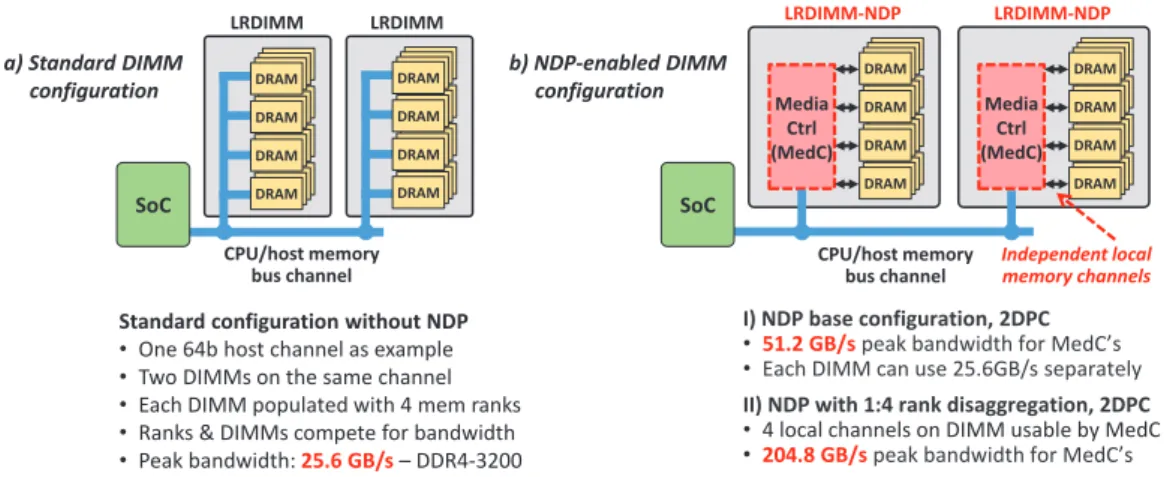
RCHITECTUREDIMM-NDP increases available bandwidth for processing by implementing NDP units locally on memory modules (DIMMs). Media Controllers (MedC), as required for forth-coming standards like NVDIMM-P [14], [15] and Gen-Z [16], are complemented with NDP units, such that DIMMs can operate independently. In addition, memory ranks on DIMM may be reorganized as independent channels on DIMM (i.e., laid out as independent channels), as visualized in Fig. 2. The required routing can be solved on PCB-level with additional routing layers, as we still rely on the ball pitch of standard DRAM devices.
3.1 Architecture Overview
An overview of the building blocks involved is shown in Fig. 3. In the host System-on-Chip (SoC), the Memory Con-troller (MC) is enhanced with a memory-mapped control and status register interface to access DIMM-NDP instances. This register interface is a proxy to the more complex regis-ter inregis-terface implemented in the Media Controller (MedC).
The MedC placed on DIMM provides a fast path to DRAM if NDP units are switched off. The host’s MC em-ploys a plain DDR4/DDR5 protocol to access main memory in this case. The fast path is configured on a rank-by-rank basis (ranks seen by the host that may be laid out as in-dependent channels on DIMM). That means, selected ranks on the host channel may use the NVDIMM-P protocol [14], [15], while all others employ plain DDR4/5.
If NDP units are enabled, the host’s memory bus em-ploys JEDEC NVDIMM-P asynchronous accesses to handle variable latency for requests issued by the host to the
DRAM DRAM DRAM DRAM DRAM DRAM DRAM DRAM DRAM DRAM DRAM DRAM DRAM DRAM DRAM DRAM I) NDP base configuration, 2DPC • 51.2 GB/speak bandwidth for MedC’s • Each DIMM can use 25.6GB/s separately II) NDP with 1:4 rank disaggregation, 2DPC • 4 local channels on DIMM usable by MedC • 204.8 GB/speak bandwidth for MedC’s Standard configuration without NDP
• One 64b host channel as example • Two DIMMs on the same channel • Each DIMM populated with 4 mem ranks • Ranks & DIMMs compete for bandwidth • Peak bandwidth: 25.6 GB/s –DDR4-3200 CPU/host memory bus channel LRDIMM DRAM DRAM DRAM DRAM DRAM DRAM DRAM DRAM DRAM DRAM DRAM DRAM DRAM DRAM DRAM DRAM LRDIMM DRAM DRAM DRAM DRAM DRAM DRAM DRAM DRAM DRAM DRAM DRAM DRAM DRAM DRAM DRAM DRAM Media Ctrl (MedC) LRDIMM-NDP Independent local memory channels CPU/host memory bus channel DRAM DRAM DRAM DRAM DRAM DRAM DRAM DRAM DRAM DRAM DRAM DRAM DRAM DRAM DRAM DRAM Media Ctrl (MedC) LRDIMM-NDP SoC SoC a) Standard DIMM configuration b) NDP-enabled DIMM configuration
Fig. 2. Overview of DIMM-NDP memory organization and advantage with DIMM-local channels, 2 DIMMs per host channel.
MC Master FSMs Ctrl/status Register IF Core
cluster clusterCore
…
clusterCore CPU/host SoC Master PHY Media Ctrl (MedC) M D M C Slave PHY IMP compute NDP compute unit CPU/host memory busDRAM DRAM DRAM DRAM DRAM DRAM DRAM DRAM DRAM DRAM DRAM DRAM Slave FSMs Light
core ACC ACC DB DB DB…RCD…DB DIMMs DIMM-local memory channel(s) NDP Register IF
LRDIMM fast path (NDP bypass)
Fig. 3. Overview of DIMM-NDP architecture utilizing shared main mem-ory with the host SoC.
corresponding ranks. Asynchronous accesses do not depend on DRAM timing nor DRAM organization (banks, pages and so on). Requests from the host are thus re-queued at the MedC. The MedC employs its own memory controller (MDMC) to schedule accesses from NDP units and accesses from the host according to DDR4/5 timing. Since mem-ory is shared between the host and the NDP units, they compete for memory bandwidth whenever accesses occur concurrently. MDMC’s scheduling policy resolves conflicts between the host and NDP units by priorities and DRAM timing parameters.
3.2 NDP Unit Setup
For versatility and energy efficiency, we consider in-order cores as programmable NDP units (similar to ARM’s Cortex-A55 core) that can be enhanced with functional units for vector and matrix processing (accelerators [ACC]). We assume that the register file for the vector unit can be reused by the matrix unit. In our evaluation setup described in section 6, the ARMv8-A [34] core for NDP uses Scalable Vector Extensions (SVE, [35]) and the specific organization of the matrix unit from [36].
An NDP unit employs a reduced memory hierarchy of one level of caches plus an optional scratchpad memory in parallel to the L1 caches. We associate one NDP unit with each local memory channel. An NDP unit may access neighboring channels on the same DIMM at slightly higher
access latency over the on-die hierarchical interconnect of the MedC chip.
3.3 Lateral Data Transfers between NDP Units
Lateral memory requests between the memory ranks and channels on the same DIMM are quick, since the MedC buffer includes the corresponding NDP units and local memory controllers (MDMCs in Fig. 3). Data requests issued by one NDP unit to other DIMMs and channels of the host can be routed through the memory controllers of the host SoC, but will be slower than local accesses. Forthcoming NVDIMM-P [14] will provide signaling channels to notify the host of pending events and actions at the DIMM side. NDP-data can be kept local on the same DIMM by, for instance, employing a NUMA-aware memory allocator to reduce the need for lateral transfers.
3.4 ECC Handling
If the NVDIMM-P [15] protocol is switched on, we assume that the Error-Correcting Code (ECC) processing is done at the media controller on DIMM, as many different types of DRAM and non-volatile memory may be used on DIMM with NVDIMM-P, requiring custom ECC methods. The host can have access to ECC event statistics that happen on the DIMM, such that this information can be used in a higher-level RAS policy (Reliability, Availability and Serviceability). If NDP is switched on, the MDMC instance (see Fig. 3) is responsible for ECC processing in our case.
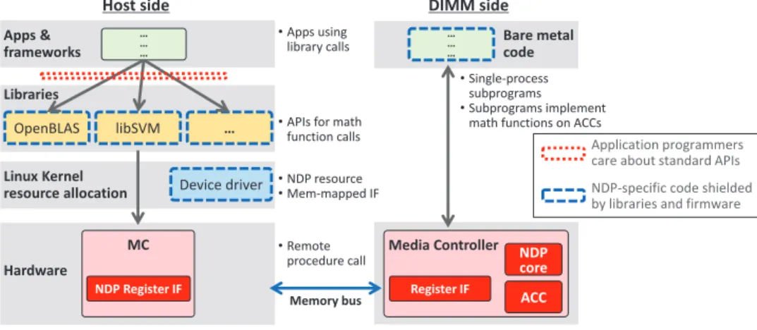
4
S
OFTWAREV
IEW OFDIMM-NDP
By building on the currently most pervasive JEDEC memory interface, hardware coherency techniques are not available. For using accelerators, this is manageable in software since programmers of scientific applications are familiar with syn-chronizing activity on CPUs and accelerators, like FPGAs and GPUs.
4.1 Workload Partitioning and Data Placement
By choosing coarser-grained programmable cores as NDP units, the degree of parallelism remains manageable. The number of cores in the host CPU and the number of NDP
Device driver Linux Kernel resource allocation • NDP resource •Mem-mapped IF Libraries
OpenBLAS libSVM … •APIs for math
function calls
•Single-process subprograms
•Subprograms implement math functions on ACCs Apps & frameworks •Apps using library calls … … … … … … Hardware •Remote procedure call MC NDP Register IF Media Controller Register IF NDP core ACC
Host side DIMM side
Memory bus
Bare metal code
NDP-specific code shielded by libraries and firmware Application programmers care about standard APIs
Fig. 4. DIMM-NDP programming abstraction on host and NDP sides and host-centric programming flow.
units are similar, such that, e.g., a pragmatic 1:1 association of host cores and NDP units for offloading may be ap-plied. Data are partitioned by the number of NDP-enabled DIMMs. This is similar to using a number of PCIe-attached accelerators and thus a well-known workable constraint for programmers of scientific applications.
The MedC buffer is in control of several local ranks on DIMM, such that an NDP unit co-located at one rank can access data on the other ranks at the same MedC. Transfers between DIMMs must go over the host memory controller (MC) by signaling events over NVDIMM-P. Programmers can influence the frequency of remote transfers by exploiting a NUMA memory allocator on the host to keep the data local, and by means like data replication, exploiting the capacity of main memory.
4.2 Protection/Virtual Address Spaces
The infrastructure for address space protection and memory management of a standard core for use with NDP remains important for limiting the scope of the NDP unit. The assumption is that the process on the host that reserved the NDP unit is also responsible for configuring the unit, such that the unit runs in the same address space as the host process. The scope of the NDP unit can be reduced by only taking over a subset of the address translation tables of the host process to the NDP side. Alternatively, the NDP core may use a reduced translation table, e.g. by employing large pages or segments as done in, e.g., [37].
Translation entries can only be changed by a process on the host that reserved the NDP resource in the first place. The NUMA memory allocator for NDP is implemented on the host, such that data structures can be set up before handing over execution to the NDP side to avoid frequent updates of the translation tables at the NDP side.
4.3 Synchronization
With DIMM-NDP, programmers may use the host as the master that triggers activity on NDP units explicitly over their register interface. Alternatively, synchronization may happen over shared memory regions in a more distributed fashion. We thus expect synchronization points defined by software, such that the memory subsystem will be in a
well-defined state by employing explicit cache maintenance operations on the host and NDP sides.
4.4 Software Implementation Flow
An NDP unit runs bare-metal in a first revision for scientific workloads and thus supports only one application context. We do not consider context switches on the NDP side, i.e., an NDP unit can only be reserved by one process on the host. We interpret “bare-metal” as bare machine computing as, e.g., applied in [38], where a self-contained Application Object includes a minimal single-execution operating envi-ronment. For instance, the NDP bare-metal code does not cover exception handling. Exceptions are handed over to the host process, either by signaling over the NVDIMM-P backchannel and/or shared memory. In our NDP context, the setup of the NDP execution environment is configured by the host process that allocated the NDP unit as a resource. Overall, migrating code to DIMM-NDP becomes straightforward, particularly if the same instruction set is supported on the host and NDP.
A functionally correct implementation can be derived quickly with bare-metal compiled code on the NDP units. Effort can then be put on iterative refinements for per-formance tuning (see study in subsection 7.4), e.g., along vectorization and using scratchpad memory. Fig. 4 provides an overview of a first release of a software setup.
Programming complexity is shielded by established math libraries that the programmer is used to. In order to re-serve and configure NDP resources, we can take advantage of the known NUMA abstraction to, for instance, co-locate data and NDP units. Each NDP-enabled DIMM appears as a separate NUMA domain. The NUMA allocator is imple-mented on the host, following a CPU-centric programming model as the host has access to the complete capacity of main memory.
5
H
ARDWARES
ETUPS FORDIMM-NDP
We distinguish module options for DIMM-NDP that sup-port 2 and 4 local memory channels on DIMM respectively. Feasibility checks are considered for JEDEC DDR4, as com-prehensive information is available for DDR4, and DDR5 is not standardized yet. We analyze two form factor options,
TABLE 1
Characteristics of Compute and Memory Building Blocks Reported in Related Work
Block Clock Technology Area Power Description
ARM Cortex-A53 core 1.8GHz TSMC FF+ 16nm 0.5mm2 200mW [39], running Dhrystone 64b mem IO frontend DDR4-3200 10nm 6 - 9mm2 400mW [40], [41] for power estimation,
[42], [43], [44] for areaa)
Scratchpad 16nm 1.5mm2 [45], for 2MB capacity
Vector unit 1GHz 40nm 4mm2 <300mW [46]: SP-FP data type, 1024b vectors
Vector unit 250MHz LSI 28nm 30mW [47]: 32b int,≤1024b vector length
Vector unit 1GHz 28nm 3.6mm2 [48]: DP-FP type, 4x128b lanes, 300KB caches
Matrix unit 700MHz 28nm ≤115mm2 <40W [49]: 8b int, 256x256 MAC array, 4MB SRAM
a)
Additional 10% to 20% area for memory controller
power and chip area requirements, as well as overhead costs for the complete modules.
5.1 Power and Area Analysis of Building Blocks Based on related work listed in Table 1, we project required area and power back-of-the-envelope. On a recent 10nm technology process, we estimate a feasible vector unit design for 512b vectors, including register file (16 to 32 vector registers), to take less than 1mm2 and consume 100mW to 200mW at 1 to 1.5GHz clock range for use by the NDP unit. Scaling down the 256x256 matrix unit of the TPU [49] to the dimensions we consider for multiply-and-accumulate (MAC) operations as a special unit, still on 28nm, we need:
16 x 16 MAC: area 0.45mm2, power: below 150mW 32 x 32 MAC: area 1.8mm2, power: below 600mW
These are upper limits, since our design will use a more recent process technology, providing us headroom for a higher clock rate and/or support of different data types. We assume that the register file for the vector unit can be reused by the matrix unit.
The area requirements for the MedC buffer chip on a 10nm-like process are summarized in Table 2 for the two DIMM scenarios of interest using two (standard DIMM) and 4 (custom DIMM) local memory channels for NDP respectively. The analog memory IO frontend blocks are the major contributing factor.
5.2 Chip Packages and Form Factors
The following analysis shows that the size of the MedC device is determined by the need for IO balls and not by the logic complexity of the buffer (see area evaluation in the preceding subsection for comparison).
5.2.1 DIMM Memory Module Form Factor and Power
The power envelope for a DDR4 DIMM is typically dimen-sioned for about 13W [50]. An LR-DIMM can hold up to 36 DRAM x4 devices, one RCD [51], and 9 DB [52] chips, employing both sides of the DIMM. An NDP-enabled MedC chip that supports two local DDR4 channels needs a 900-ball package estimated from prior art (Intel SMB [53], JEDEC DDR3 MB [32] and JEDEC AMB [33]). At a 0.8mm ball pitch as used by DRAM devices, such a package requires roughly 25mm x 25mm or a rectangular layout. This package fits
on a standard DIMM with about 28mm usable height. A standard DIMM has enough room for 18 x8 DRAM devices, x8 DBs and the NDP-enhanced MedC, using both sides of the DIMM as sketched in Fig. 5 a).
Example a) horizontal placement, x8 devices, 32GB, DIMM form factor, 2 local channels, 2Tops, 13W
Example b)vertical placement, x4 devices, 128GB, custom DIMM height, 4 local channels, 16Tops, 40W Fig. 5. DIMM-NDP modules: a) standard, b) custom DIMM form factors.
5.2.2 Accelerator Form Factor (Custom DIMM) and Power
A custom form factor allows higher design power, e.g., 40W, but needs additional power lines and cooling. This is the option for highest performance and capacity. Example: 4 channels with x4 DRAM need 72 DRAM devices, requiring roughly double the regular DIMM height using both PCB sides, see Fig. 5 b). Alternatively, 4 channels with x8 DRAM need 36 DRAM devices that can be arranged in 3 rows, such that only about 10mm extra height is needed. The MedC chip package roughly needs a 1500-ball package as estimated from prior art (e.g., IBM Power8 buffer [54]). The package takes 32mm x 32mm area at 0.8mm ball pitch and 26mm x 26mm area at 0.65mm pitch respectively.
5.3 Resulting NDP-enabled Memory Modules
The following NDP-enabled modules use the estimations from the previous subsections. DRAM device power is derived from Micron’s DDR4 device power models [41] at 100% utilization with 2/3 reads, 1/3 writes (no power down cycles), open-page mode, 50% hit rate, 50% bit toggle rate.
5.3.1 NDP on Regular DIMM within 13W at 32GB
In this setup, the MedC embeds two in-order cores with their vector and matrix units to support two local DRAM channels at 51GB/s peak bandwidth for DDR4-3200. With 16Gb DRAM x8 devices, the total capacity of the DIMM is 32GB. The power envelope stays within 13W based on the conservative estimation in Table 3.
TABLE 2
Area Estimation of NDP Building Blocks on 10nm-like Technology Process for MedC Buffer Chip
Standard DIMM Custom DIMM
Block Area Quantity Total Area Quantity Total Area
In-order core with L1 caches 1mm2 2 2mm2 4 4mm2
Vector unit, 512b 1mm2 2 2mm2 4 4mm2
Matrix unit (16x16|32x32) 0.5mm2|2mm2 2 1mm2 4 8mm2
Glue logic (MDMC, buses, etc.) 4mm2 2 8mm2 4 16mm2
Memory IO frontend 9mm2 3 27mm2 5 45mm2
Optional scratchpad 1.5mm2 2 3mm2 4 6mm2
NVDIMM-P asynchronous accesses 2mm2 1 2mm2 1 2mm2
Estimated MedC chip area (sum) <45mm2 <85mm2
TABLE 3
Power Analysis of NDP on standard and custom DIMMs, logic at 2GHz on 10nm-like Technology Process Standard DIMM Custom DIMM
Block Power Quantity Total Quantity Total Note
In-order core 0.3W 2 0.6W 4 1.2W
Vector unit, 512b 0.3W 2 0.6W 4 1.2W
Matrix unit, 16 x 16 0.3W 2 0.6W 2Tops total (MAC counting as 2 ops)
Matrix unit, 32 x 32 1.2W 4 4.8W 16Tops total (MAC counting as 2 ops)
Glue logic 2W 1 2W 2 4W MDMCs, on-die buses, FSMs, etc.
Mem IO frontend 0.4W 3 1.2W 5 2W local channels and interface to host
x8 DRAM device 0.4W 18 7.2W including ECC, DDR4-3200
x4 DRAM device 0.32W 72 23W including ECC, DDR4-3200
Discrete DBs (if needed) 0.8W 1 0.8W 1 0.8W mainly 2x memory IO frontend
Estimated DIMM total power (sum) 13W 37W
5.3.2 NDP Accelerator Form Factor≤40W, 128GB
The MedC embeds 4 cores, each with one 32x32 MAC array and one vector unit, to support 4 local DRAM channels at 102GB/s bandwidth for DDR4-3200. With 16Gb x4 devices, we reach 128GB capacity, staying below 40W (Table 3). 5.4 Cost Analysis for Memory Module
Cost factors vary depending on specific supply chains, i.e., the following should be seen as indicative only. Assuming a volume of 1 million DIMMs, non-recurring engineer-ing (NRE) costs can be neglected for the most part. This corresponds to about 60k fully populated sockets, which we consider as low volume and realistic to achieve. We recognize the following factors that limit additional costs to less than 20% by switching from LRDIMM to DIMM-NDP:
• PCB layout with additional routing layers: Overhead is less than $10 per board (see [55] for an overview of PCB cost factors).
• MedC buffer chip: Additional costs are below $30 since the buffer has a similar complexity as a smartphone chipset [56].
• DRAM costs: Stay the same. At $7/GB1, costs for 128GB plus ECC are about $1000.
• Cooling and power distribution: the 128GB DIMM-NDP can still be cooled by air flow (16 boards, 40W each, equal two “heavy” PCIe boards); overhead of a few dollars per board.
1. DRAM spot price, as of Dec. 2018 tracked at DRAMeXchange: https://dramexchange.com/
DRAM costs remain the dominating factor of the DIMM. In comparison, solutions based on HBM and HMC are up to one order of magnitude more expensive than DDR4 at the same capacity due to TSV processing steps and TSV area for heterogeneous stacking, testing and package costs [57]. [58] suggests a price premium of about 3x for HBM2 over GDDR5. In addition, we have to factor in the costs for custom logic for each stack to support NDP units in a heterogeneous 3D stack or have to consider a wide memory interface in the media controller. Silicon interposer costs for integrating HBM are at the same level as the costs for the buffer chip stated above due to the required area.
6
E
VALUATIONS
ETUP ANDF
LOW6.1 Selected Workloads
In order to characterize DIMM-NDP, we complement low-level benchmarks for memory bandwidth and latency with full applications from the domain of data analytics, scientific computing and machine learning as representatives of a wider range of compute methods.
6.1.1 Elementary Tests
• stream [6] stresses memory bandwidth for 4 different matrix compute kernels.
• Pointer chasing, as in lmbench [60], reveals round-trip memory latency under low load.
TABLE 4
Characteristics of Selected Data Sets for liblinear and libSVM Applications
Name Type Classes Samples Features
Features/
Use case sample [avg.]
News20.binary sparse 2 20K 1.4M 462 text classification in newsgroups
Avazu sparse 2 40M 1M 15 click-through prediction for ads
Protein sparse 3 18K 357 102 protein structure prediction
e2006-tfidf sparse 8 16K 150K 1218 financial risk assessment
YearPredictMSD dense 86 463K 90 90 year of song prediction by audio features TABLE 5
Host SoC Configuration as Reference
Parameter Description
Core count up to 48 ARMv8-A [34] out-of-order
Core type ARM Cortex A76-like [59] (decode width 4, 16 SP-FLOPS/cycle), AArch64 state Core frequency 3GHz
HW prefetcher stride prefetcher on I$ (degree 1), D$ (degree 4) and L2 (degree 8) L1 cache 64KB I$ and 64KB D$ per core
L2 cache 512KB per core, private
Last Level Cache up to 48MB exclusive with L2$’s Main memory 8 channels at DDR4-3200
MC memory control FR-FCFS (first row hit – first come first served); open adaptive open-page mode Interconnect 2 bi-directional rings, 16B/clock per direction
PCIe IO 32 available PCIe gen4 lanes for accelerators
6.1.2 Applications
Kaggle’s survey on the state of data science [61] reveals methods like logistic regression, neural networks and de-cision trees in the top-5 of the most popular techniques. We choose representative workloads from this set that span memory and compute-bound programs.
• liblinear [62] for solving linear classification and re-gression. The solvers rely on Level-1 vector Basic Lin-ear Algebra Subprograms (L1 BLAS) and are memory bandwidth-bound.
• libSVM [63] for solving support vector classification, regression, and multi-class classification. The solvers rely on L1 BLAS vector operations and are memory bandwidth-bound.
• SSD[64] (Single Shot MultiBox Detector) applies convo-lutional networks for the detection of multiple objects in images. SSD relies on Level-3 BLAS matrix operations and is more compute than memory-bound.
• xgboost [65] addresses classification and regression problems with gradient boosting by employing deci-sion trees, relying on tree traversals, and is memory latency-bound.
6.1.3 Data Sets
The data sets in Table 4 are selected forliblinearandlibSVM and listed at the libSVM page ( [63], from various sources). These represent different set sizes and feature sets. The number of samples are shown for training. Additional 10% to 20% are usually available for testing.
For SSD, we apply the SSD300 model with the Pascal VOC07+12 dataset referenced at the SSD webpage [64] for training the object class recognition in images.
For xgboost, we use the kaggle-higgs competition for identifying Higgs bosons (250k events with 30 features) and the YearPredictMSD data sets. Both are referenced in the xgboost distribution [65].
6.2 System Configuration
6.2.1 Host SoC
Inspired by recent high core-count CPUs like Qualcomm Centriq (48 cores), Marvell ThunderX2 (32 cores), AMD EPYC (32 cores) and Intel Xeon Scalable Processor (28 cores) and their memory subsystems, we consider the reference system in Table 5 as host SoC.
6.2.2 NDP Unit
The parameters for one NDP unit are summarized in Ta-ble 6, including vector, matrix and scratchpad support. Considering up to 2 DIMMs per host memory channel and four ranks per DIMM, we can have up to 64 NDP units per host SoC socket.
6.2.3 Mapping from System-physical to
DIMM/DRAM-physical Addresses by the Host
As in related work [19], [67], address interleave between DRAM banks, ranks and channels on cacheline granularity on the host memory bus has to be adapted to keep data local to NDP units. In our case, fine-grain address interleave be-tween DIMMs and host channels should not be applied for NDP-enabled memory ranks. The MedC buffer on DIMM may apply any address interleave scheme for the ranks and banks under its control to reach higher utilization.
TABLE 6
Configuration for one NDP Unit
Parameter Description
Core type ARMv8-A [34] in-order, ARM Cortex A55-like pipeline, AArch64 state Core frequency 2GHz
Vector support SVE512-like [35]
Matrix support 16 x 16 single-precision Floating Point MAC array [36] Memory single channel at DDR4-3200
MDMC mem control FR-FCFS (first row hit – first come first served); open adaptive open-page mode L1 cache 32KB I$ and 64KB D$ per core
Scratchpad optional 2MB
TABLE 7
Energy per Elementary Operation on 10nm-like Process Extrapolated from [4], [5], [40], [66]
Operation Host: High-freq NDP: Low voltage Description process [pJ] process [pJ]
Exec, 1 instruction 110 (OoO) 13.1 (InOrder) complexity of control logic, I$
Idle 40 (OoO) 10 (InOrder) factoring in IPC, CLK, leakage
Integer simple / complex 0.1 / 3 0.07 / 2.2 Int Add / Int Mul
FP simple / complex 0.9 / 3.7 0.7 / 2.8 FP Add / FP Mul
SIMD Int simple / complex 0.2 / 6 0.15 / 4.5 128b width SIMD FP simple / complex 1.8 / 7.4 1.3 / 5.5 128b width
SVE vector instruction (4x) 512b: 4x the value of 128b SIMD instr
D$ read 20 17 64b value
L2$ read 170 512b, includes wiring
LLC read 400 512b, includes wiring, on-die buses
DRAM access (DIMM) 3 to 10 pJ/bit typ. depending on operating pointa) DRAM access (IO) 1.1 to 1.7 pJ/bit for address, cmd, data linesa)
DRAM background power 93 mW for each x8 device refresh overhead & active standby [41] a)DRAM read & write percentage, DRAM page hit & further statistics derived from simulation
in Gem5 and used with the DDR4 Micron power model [41] for x8 devices at DDR4-3200
6.3 Evaluation Flow
6.3.1 Performance Evaluation
The Gem5 simulator [68] is used as framework in system emulation mode. We added the following enhancements to model the features described in subsection 6.2:
• The out-of-order core model is calibrated to match the performance level of a modern core in terms of issue width, internal bandwidth, queue depths and functional units
• We derived the NDP unit model from a Gem5 branch that models vector instructions (SVE [35]) and added SVE gather/scatter support
• NVDIMM-P-like asynchronous communication
be-tween the host and NDP core systems is modeled by a bridge block between the two subsystems
• We implement the matrix unit as additional functional unit that reassigns selected SVE command encodings for use with the unit (a real implementation requires new instructions)
• We model the impact of cache maintenance by ARM cache-clean & invalidate operations on virtual ad-dresses (thus covering all cache levels on the host) on the host and the NDP sides
We use ARM’s compiler for HPC, release 18, as starting point for SVE-enabled assembly, as well as the ARM
Instruc-tion Emulator (ArmIE) for funcInstruc-tional verificaInstruc-tion of the SVE implementation.
For partitioning the execution of the workload onto the host and DIMM-NDP, we split the workload into execution phases where either the host or the NDP side is active on the working set. In this way, we can manage synchronization with spinlocks on shared memory in software and rely on explicit cache maintenance for consistent data. In order to determine these phases, we profile the workloads on real x86 and ARM servers and not in simulation to:
a) Derive the number and length of the phases for the complete workloads
b) Assess and characterize the loss of scalability due to parallel overhead (such as communication and syn-chronization) at high core and NDP unit counts, where appropriate depending on the programming approach With performance counters, we determine hot code sec-tions. We further classify these into CPU and memory-bound sections by using LLC statistics, such as MPKI and LLC usage. We prefer offloading procedures to NDP, either at low level (e.g., for batches of BLAS1 dot product calls in libSVM) or at higher level (e.g., for calls of the optimization solver in liblinear).
6.3.2 Energy Evaluation
We use activity counters to project energy efficiency with annotations for logical and memory operations for recent 10nm-like process technology by extrapolation from [4], [5], [40], [66], see Table 7. We use these for ranking alternatives for design-space exploration, but not for absolute results. We do not consider energy consumption related to waiting for acquiring a spinlock. Spinlocks are the mode of operation for this case study, but can be improved by, e.g., explicit sig-naling and power down phases triggered over the DIMM-NDP register interface.
7
P
ERFORMANCEE
VALUATION OFDIMM-NDP
This section describes results for performance evaluation of DIMM-NDP based on simulation of the microarchitecture in a system setup with selected workloads, as well as an assessment of the software porting effort to reach the reported performance.
7.1 Performance and Efficiency Results
7.1.1 Model Calibration
We use the elementary stream and lmbench tests (subsec-tion 6.1) to align achievable latency and bandwidth by our core models with existing designs.
7.1.1.1 Host “Big” Core: The round-trip latency for read accesses under light load as determined by pointer chasing on main memory reaches about 270 core clock cycles (90ns), which is about 10% to 20% worse than for an high-end server, representing a mid-range setup. Similarly, latencies for the cache levels are set based on measurements on real systems (several Intel Xeon v3 and v4 processor sys-tems, ARM Juno R2 board with ARM Cortex-A72, Huawei TaiShan 2280 ARM server with HiSilicon Kunpeng 916, and APM X-C1 evaluation boards).
7.1.1.2 NDP “Little” Core: The unloaded latency to main memory derived from pointer chasing reaches about 115 core clock cycles (58ns) mainly due to a reduced mem-ory hierarchy compared to the big core setup. As expected, the usable bandwidth from main memory for the little core much more depends on efficient prefetching, either in hard-ware or softhard-ware, but can reach the same level of utilization as the big core of about 85% for stream and BLAS1 kernels with the use of the vector unit. The effort for this kernel-specific tuning will be discussed in subsection 7.4.
7.1.2 Kernel-level Performance
We apply isolated single unit models for the host SoC and the NDP unit to evaluate compute kernels. Assuming a balanced symmetric use of the units, we then extrapolate full system performance by the number of units that can work independently (up to 48 cores on the host, up to 64 NDP units in the memory subsystem with 8 channels if 4 ranks per DIMM and two DIMMs per channel are used). For the host model, we restrict the available memory bandwidth and LLC capacity for one core to1/nthof the host’s memory bandwidth and LLC capacity, withnrepresenting the total core count we want to extrapolate performance for. For one NDP unit, on the other hand, we assume that the unit can exploit the full bandwidth of one memory channel locally on
the DIMM. We exclude initialization time of data structures from the execution time of kernels. We consider a dataset-dependent warmup phase in simulation such that we reach a steady state, both for the use of data (e.g., weight vectors) and the architecture model (e.g., branch predictor state).
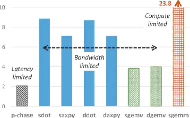
23.8 0 2 4 6 8 10
p-chase sdot saxpy ddot daxpy sgemv dgemv sgemm Latency limited Bandwidth limited Compute limited
Fig. 6. DIMM-NDP speedup over host CPU for compute kernels, extrap-olated from single-unit models.
Fig. 6 shows the speedup for compute kernels on DIMM-NDP compared to the host for 8 DIMM-NDP units per memory channel. Pointer chasing (p-chase) is latency-limited and benefits from the smaller memory hierarchy of NDP.dotand axpy are BLAS level 1 kernels (vector - vector operations), gemv BLAS level 2 (matrix - vector ops), and gemmBLAS level 3 (matrix - matrix ops) kernels respectively for either double (d) or single (s) precision floating-point operations. sgemmtakes advantage of the matrix unit (dimension 16x16 considered for the evaluation).
BLAS-L1 kernels are limited by memory bandwidth and thus take full advantage of the additional bandwidth offered by DIMM-NDP.sgemmbenefits from matrix operations and is rather limited by computations. sgemm could scale fur-ther for larger matrix units.
7.1.3 Performance of Applications
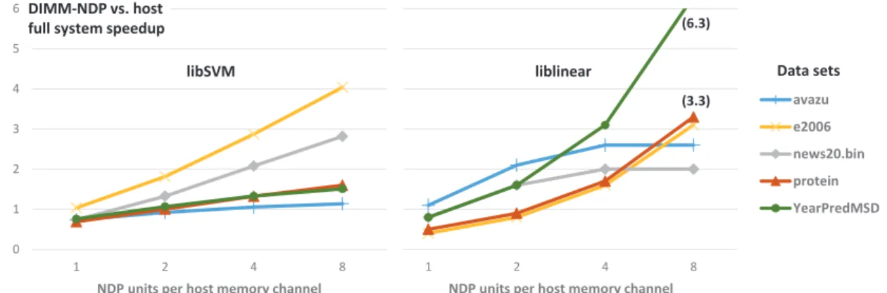
We employ a full-system simulation model, coupling the model of the host with the model of NDP computing by a custom bridge block that allows both sides to operate on shared memory, while the host model has to adhere to NVDIMM-P-like timing. Also, as for the kernel results, the host model is subject to scaled-down bandwidth depending on the number of active cores at the host side. Fig. 7 shows the relative performance forlibSVMandliblinearfor different numbers of NDP units per host memory channel. The selection of the right version of a compute kernel (e.g., degree of unrolling and prefetching) is dataset-dependent. The software optimizations are described in more detail in subsection 7.4.
Forliblinear, we offload the full solver to NDP. Dataset YearPredMSD can take advantage of kernels that are tuned for dense data structures and scales best, coming close to the results of the kernels shown in Fig. 6. The speedup for datasets avazu and news20.bin flattens out for liblinear, since the degree of parallelism is limited by the number of 10 concurrent cross-validation runs and number of classes cho-sen for this setup. Results are shown for solver 1 (support vector classification). We also evaluated solver 0 (logistic regression) that led to similar results (see section 7.4).
0 1 2 3 4 5 6 1 2 4 8
NDP units per host memory channel
avazu e2006 news20.bin protein YearPredMSD 0 1 2 3 4 5 6 1 2 4 8
NDP units per host memory channel
libSVM liblinear
DIMM-NDP vs. host
full system speedup (6.3)
(3.3)
Data sets
Fig. 7. DIMM-NDP speedup over host CPU for libSVM and liblinear applications, full system.
ForlibSVM, we exploit concurrency by distributing sets of samples to different NDP units on a more fine-grain level than for liblinear, based on the code structure. Since each sample may contain a different number of features, balancing the load of the units becomes more challenging, requiring dynamic workload distribution for best results. Datasets with a limited number of features per sample (YearPredMSD, avazu, protein) show reduced scalability since the time spent in the BLAS L1 dot kernel is limited, thus increasing the effort for managing the samples com-pared to the host.
ForSSD, about 95% of the time on the host is spent in the convolutional layers that depend by 90% on the execution of thesgemmBLAS L3 kernel. By employing the matrix unit and optimizing the data reorganization stage for performing convolutions with matrix multiplications, we are able to achieve a speedup of5.1. The assumption is that NDP units run independent SSD instances.
TABLE 8
NDP Scratchpad Speedup for liblinear
Dataset News20 Avazu Protein e2006 YearPredictMSD
Speedup 1.94 1.96 1.08 1.68 1.10
7.1.4 Impact of Using the Scratchpad
Table 8 summarizes the speedup for liblinear for using a scratchpad vs. relying on the L1 cache only. For this sensi-tivity analysis, we approximate the behavior of a scratchpad with a fully associative cache in parallel to the L1 cache that is responsible for a separate memory region (i.e., data placement in memory determines the right cache). For the scratchpad version, we can remove much of the L1-specific prefetch code in favor of bulk transfers to the scratchpad. The scratchpad appears favorable for datasets where a de-cent number of features can take advantage of the locality offered by the scratchpad.
7.1.5 Energy Efficiency
Employing activity counters (see subsection 6.3), the relative energy required by BLAS L1 and L2 kernels for different vector and matrix sizes is shown in Fig. 8. The baseline is the corresponding execution on the host processor. The
reduction of required energy is mainly due to fewer accesses in the memory hierarchy triggered by cache maintenance operations between cache levels. On kernel level, we recog-nize a 3x to 4x potential for reducing energy.
0.0 0.2 0.4 0.6 0.8 1.0 blas1.1000000.daxpy blas1.1000000.ddot blas1.1000000.saxpy blas1.1000000.sdot cold_caches.10000x5000.dgemv cold_caches.8x2000.dgemv cold_caches.10000x5000.sgemv cold_caches.8x2000.sgemv warm_caches.10000x5000.dgemv warm_caches.8x2000.dgemv warm_caches.10000x5000.sgemv warm_caches.8x2000.sgemv Lower is better Baseline (host)
Fig. 8. NDP kernel-level reduction of energy for BLAS L1 and L2 kernels and different vector and matrix sizes.
On application-level, Fig. 9 shows the efficiency results for DIMM-NDP relative to complete execution on the host for liblinear and the selected datasets for our full system setup. We attribute 4x the energy for IO signaling from the host compared to direct access by an NDP unit due to our setup with 2 DIMMs per channel and buffers on DIMM. If we reduce this factor to 2x, the results are impacted by less than 3%. The reduction potential by 2x to 3x can thus mainly be attributed to the efficiency of the BLAS Level 1 kernels.
0 0.2 0.4 0.6 0.8 1 avazu e2006 news20bin protein yearpred Lower is better Baseline (host)
Fig. 9. NDP application-level reduction of energy for liblinear and differ-ent data sets.
7.2 Comparison of Near Main Memory Processing vs.
Loosely Coupled Accelerator
We perform a sensitivity analysis of the number of syn-chronizations between the host and NDP units on the
TABLE 9
Coupling Characteristics between Host SoC and NDP Units with Different Interface Options for NDP.
Configuration Peak bandwidth Host latency Capacity Peak NDP-local Note
to/from host to NDP memory bandwidth
Standard DIMM, 2DPCa)
205GB/s <200ns 512GB 0.8TB/s host shared memory
Custom DIMM, 2DPCa)
205GB/s <200ns 2TB 1.6TB/s host shared memory
NDP over PCIe 63GB/s µs range ≤512GB ≤1.6TB/s extra DRAM costs
NDP over reduced PCIeb)
63GB/s 0.5µs range ≤512GB ≤1.6TB/s extra DRAM costs
a)
2 DIMMs per channel b)Such as latency-optimized Gen-Z [16] or CCIX [17]
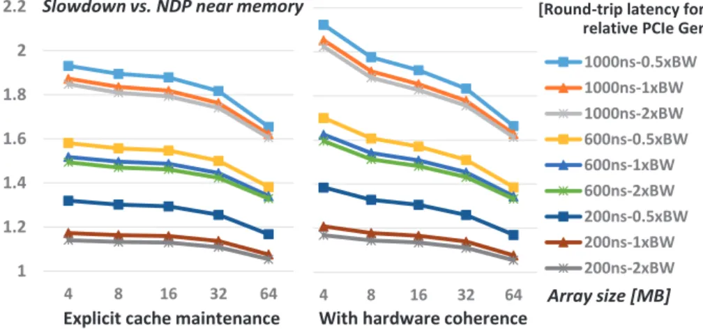
1 1.2 1.4 1.6 1.8 2 2.2 4 8 16 32 64 1000ns-0.5xBW 1000ns-1xBW 1000ns-2xBW 600ns-0.5xBW 600ns-1xBW 600ns-2xBW 200ns-0.5xBW 200ns-1xBW 200ns-2xBW 1 1.2 1.4 1.6 1.8 2 2.2 4 8 16 32 64
Slowdown vs. NDP near memory
Explicit cache maintenance With hardware coherence
Array size [MB]
[Round-trip latency for 64B packet – relative PCIe Gen4 bandwidth]
Fig. 10. Slowdown of PCIe setup vs. DIMM-NDP near main memory for pointer chasing workload and varying array sizes.
performance of DIMM-NDP and a loosely PCIe-attached accelerator with the same NDP units and memory capacity. In this way, we characterize the impact of tight vs. loose coupling on overall performance to position DIMM-NDP relative to more established solutions. The comparison is optimistic for the PCIe accelerator since memory must be allocated on the card, usually at lower capacity than the main memory of the host. Additional data partitioning and bulk copying between the host and the accelerator required in this case are not considered here.
7.2.1 PCIe NDP Setup
The DIMM-NDP advantage in terms of bandwidth and latency compared to PCIe for working with the host is summarized in Table 9, considering parameters from Ta-bles 5, 6 and subsection 5.3. For phases where the host and NDP units have to synchronize, our DIMM-NDP solution in main memory should have an up to 3x advantage in terms of bandwidth (if data are copied; by applying cache maintenance, the advantage is higher) and up to 10x in terms of latency. We use pointer chasing as a stress test to highlight the impact of synchronization/communication between the two sides. Arrays are initialized with random access patterns by the host for use with pointer chasing by the NDP units. For the NDP PCIe setup, the arrays have to be copied to the NDP unit after initialization, whereas for NDP in main memory the host performs cache-clean operations. The results of the tests are communicated back to the host accordingly.
4000 6000 8000 10000 12000 100 120 140 160 180 200 220 str e a m co p y b a n d w id th [M B /s ]
lmbench Round-Trip unloaded latency [ns] Same COD
Neighbor COD
COD on remote socket, best case
COD on remote socket, worst case
Each CPU socket contains 2 Clusters-on-Die (COD) that are exposed as NUMA domains
Fig. 11. Degradation of memory access latency and bandwidth with distance between allocated NUMA nodes for compute and memory, on Intel Xeon E5-2660v3 processor based dual socket server.
7.2.2 PCIe NDP Results
Fig. 10 presents the results for the pointer chasing test. We distinguish two coherence methods. The results on the left depend on explicit cache maintenance operations to clean caches on either the host or the NDP side. This represents the mode of operation that we use with DIMM-NDP as well, and models the use of classic PCIe. The results on the right rely on hardware coherence to keep data consistent and thus represent future interfaces like CCIX [17]. We change the round-trip latency and peak bandwidth to provide a sensitivity analysis of these parameters, thus covering the potential of protocol stacks for Gen-Z [16] and CCIX [17].
By varying the array size for pointer chasing, we change the ratio of time spent on the host for initializing the
0.0 0.2 0.4 0.6 0.8 1.0 1.2 1.4 1.6
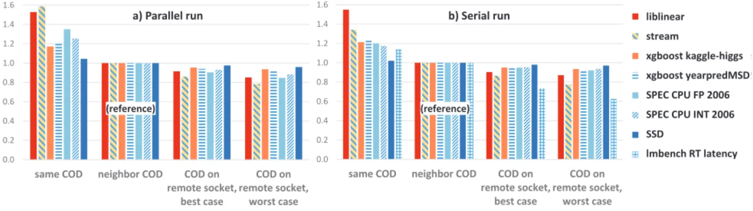
same COD neighbor COD COD on remote socket, best case COD on remote socket, worst case liblinear stream xgboost 0.6 kaggle-higgs xgboost 0.6 yearpredMSD SPEC FP 2006 SPEC INT 2006 SSD 0.0 0.2 0.4 0.6 0.8 1.0 1.2 1.4 1.6
same COD neighbor COD COD on remote socket, best case COD on remote socket, worst case liblinear stream xgboost 0.6 kaggle-higgs xgboost 0.6 yearpredMSD SPEC FP 2006 SPEC INT 2006 SSD lmbench RT latency (reference) (reference) b) Serial run
a) Parallel run liblinear
stream
xgboost kaggle-higgs xgboost yearpredMSD SPEC CPU FP 2006 SPEC CPU INT 2006 SSD
lmbench RT latency
Fig. 12. Degradation of workload performance on Intel Xeon E5-2660v3 processor based dual socket server depending on the allocation of NUMA nodes for compute and memory.
array vs. time spent on NDP for traversing the array by pointer chasing. The baseline (DIMM-NDP) is at least 60% faster than the implementation on the host, i.e., DIMM-NDP performs better, even though the host and NDP units have to synchronize data on a fine time scale. Fig. 10 reveals a slowdown of up to 2x compared to DIMM-NDP for the PCIe cases, effectively slowing down the benchmark compared to the host for selected configurations. We can also see a slight slowdown for the configurations with hardware coherence compared to explicit cache maintenance, whereas explicit cache maintenance requires more programming effort.
7.2.3 Discussion of Near-Data Interface
The DIMM-NDP implementation for this setup is limited by serializing synchronization and computing. The synchro-nization can further be reduced by switching from using spinlocks on shared memory to a more direct signaling path controlled by the host over the memory-mapped register interface of the NDP units.
Cache maintenance over levels of the memory hierarchy on the host becomes a limiting factor for fine-grain preserva-tion of consistent data, since the processing cores can either compute or do cache maintenance. This is seen in Fig. 10 for small array sizes, as more frequent interactions between the host and the NDP units are needed. The characteristics in Table 9 suggest at least an advantage of 4x for DIMM-NDP over the PCIe configuration for exchanges with the host, whereas the results rather converge to a factor of two. Overall, tighter coupling with the host by employing DIMM-NDP enables more host-centric usages, since smaller kernel calls can be offloaded to NDP units to achieve better performance. This setup also enables a more gradual tran-sition to using accelerators by offloading more and more functions to DIMM-NDP on shared memory.
7.3 Slowdown of Workloads Running Mainly on the
Host due to NVDIMM-P Asynchronous Accesses
In order to characterize the impact of additional latency introduced by NVDIMM-P asynchronous accesses on per-formance for workloads running mainly on the host, we perform a sensitivity analysis of latency on two 2P servers (Intel Xeon E5-2660v3 processor and Huawei TaiShan 2280) by placing compute in one NUMA domain and all memory in a different NUMA domain, e.g., on a remote socket or
different cluster-on-die (COD). Fig. 11 shows the charac-terization by our elementary bandwidth and latency tests using one running instance on the x86 server. For repro-ducible measurements, turbo mode, hyperthreading, active and idle power savings states are switched off. As placing the NUMA nodes for compute and memory on the same COD has a more than linear advantage (bypassing any interconnect bottleneck between CODs) over configurations with higher distance, we select the “neighbor COD” config-uration as reference in the following comparison.
Fig. 12 shows the speedup of workloads depending on the distance between the allocated NUMA memory and compute nodes. A parallel run is confined by the number of cores in one NUMA domain, 5 cores in our case. Beside the elementary tests, liblinear reveals the largest slowdown of the workloads, corresponding to about 3% for every 10ns of latency added, whereas all others degrade by less than 1.1% for every 10ns of latency added. This is in-line with the study by Clapp et al. [69] who estimate up to 3.5% of CPI increase for every 10ns added. Trends on the Huawei TaiShan server are less pronounced, since the reference configuration already incurs higher latency.
We expect the asynchronous access mode of NVDIMM-P to add 10ns to 20ns of latency, since the host’s memory controller has to pull data from the DIMM’s buffer after the availability is signaled by the buffer. Also, our MedC architecture introduces arbitration in its memory controller MDMC before accesses from the host reach main memory, adding up to about 50ns latency overall. As mitigation for workloads that do not share data with NDP, hybrid chan-nel configurations for the host memory bus are possible: Defined ranks and DIMMs may only be used by the host directly with the DDR4/5 protocol for best performance using the abundant memory capacity of main memory. NVDIMM-P can be enabled rank-by-rank, co-existing with native DDR4/5 accesses on the same host channel.
In our gem5 simulation model, as memory-bound phases are offloaded to NDP and do not depend on the host bus, the overall slowdown due to NVDIMM-P latency on the host bus (by sensitivity analysis of our bridge block in gem5) becomes negligible at less than 1% for liblinear.
a) Compilation: 55 cycles/iteration
b) Manually reordered: 44 cycles/iteration
Clock cycles
Micro-architecture
building blocks
Fig. 13. Dreams [70] screenshot showing microarchitecture events over time before and after manual instruction reordering for a compute loop. The number of cycles per iteration can be reduced by 20% in this example.
7.4 Software Porting Effort to Use DIMM-NDP
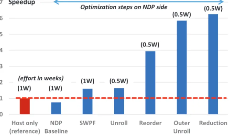
In order to reach the reported performance of DIMM-NDP, we iteratively refined the software implementation on the NDP side to take full advantage of data parallelism. The case study underpins the potential of several tuning steps to reach better performance on NDP’s in-order core and its vector unit. This can be used as a proxy for estimating the effort for providing customized application-specific libraries for use with DIMM-NDP.
7.4.1 Optimization Steps
We distinguish the following optimization steps to quantify the development effort for particularly tuning the hot BLAS L1 kernels:
• Host-only reference: Optimization of data layout to struct-of-arrays and loop fusion to simplify vectoriza-tion, using baseline version on the host
• NDP baseline:Splitting workload into execution phases based on profiling, implementing spinlocks to establish handover between phases
• SWPF: Analyzing performance, adding software prefetches, tuning memory access patterns
• Unroll: Experimenting with several unrolling sizes & analyzing instruction scheduling
• Reorder:Manual instruction reordering
• Outer unroll: Outer loop unrolling with adaption of prefetching and order of instructions
• Reduction: Optimization of vector reductions, using predication and register blocking
Note that the effort for parallelization on several NDP units is part of the first two steps and rather straightforward, as the degree of parallelism is similar to the parallelism of the number of cores on the host side. That means, we can
take advantage of profiling results and best-known methods on a high-core-count CPU to check the partitioning for NDP. As the optimization phases may reveal subtle side-effects on a small scale between the microarchitecture blocks of our NDP architecture, we use a custom version of the Dreams tool to trace and track performance effects on cycle gran-ularity together with our gem5 simulation models. Fig. 13 shows an example, where Dreams enables cycle-by-cycle optimization by displaying the impact of manual instruction reordering, as we trace the stages of the processing pipeline.
7.4.2 Porting Results
The following study summarizes the effort for the dataset YearPredMSD. Fig. 14 shows the impact of the optimization steps on the overall speedup that we are able to achieve for the logistic regression solver. Most of the effort of about one man-month has to be invested only once for establishing a domain-specific library with common compute kernels, like BLAS for linear algebra. Then, the application programmer can mainly focus on the data layout and partitioning for NDP. In this way, the programmer can start with a working, host-centric implementation and gradually move function-ality to NDP to tune performance.
7.5 Discussion of Further NDP Variants
7.5.1 PCIe Accelerator vs. near Main Memory
We think that near-memory processing at shared memory of the main host SoC allows accelerating CPU-centric pro-cessing where “big” cores can continue to shine, e.g., for us-ing interpreted and dynamic languages (python, scriptus-ing, etc.) and rich runtime environments (Java, perl, etc.) with frequent calls of kernels, like the compute “dwarfs” [71]. We can take advantage of established programming abstrac-tions for heterogeneity, such as NUMA and domain-specific
![Fig. 1. Reported Stream [6] bandwidth on system-level, annotated with architecture modifications to sustain memory performance.](https://thumb-us.123doks.com/thumbv2/123dok_us/10226257.2926468/3.892.66.436.372.594/reported-stream-bandwidth-annotated-architecture-modifications-sustain-performance.webp)
![Fig. 13. Dreams [70] screenshot showing microarchitecture events over time before and after manual instruction reordering for a compute loop](https://thumb-us.123doks.com/thumbv2/123dok_us/10226257.2926468/15.892.168.719.116.485/dreams-screenshot-showing-microarchitecture-events-instruction-reordering-compute.webp)