LOW POWER AND HIGH PERFORMANCE SERIAL
COMMUNICATION INTERFACES FOR ON-CHIP
INTERCONNECTS
Charles Rajesh Kumar J*
Dr S. Kishore Reddy**
ABSTRACT
This paper presents two novel methods for on-chip serial communication whereby the
clocks of the transmitter and the receiver are generated with two separate ring
oscillators. These oscillators are identical although they can have some a small
frequency difference. In the first method, a strobe line, which toggles exactly once with
every frame of n-bit data, is used to activate the oscillators. Local counters are used to
count the number of bits in the data frame and to stop the local oscillators when the frame
is processed. In the second method, a single physical line is used to transmit both data
and (in- band) control information, further reducing the power dissipation. The data
transmission is controlled by the output of a starter flip-flop, indicating the empty/full
status of an input buffer whereas the data reception is controlled by decoding a ‘1”
start bit and a ‘0’ end bit which have been added to the n-bit data word to form a frame.
Our circuit simulation results demonstrate that both communication methods result in high
bandwidth and low power dissipation.
Keywords: Low-Power Communication; Chips Communication; Serial Communication;
Metastability Error.
I.
Introduction
While gate delays scale down with migration to technology nodes with smaller minimum feature sizes,
delays of global wires typically increase or at best remain constant (if an appropriate number of repeaters
are inserted on the wires). In addition, although the computation energy cost is decreasing, the
communication energy cost is increasing. In a 50nm CMOS process technology, the chip die will
be about 22mm on each side with a global wire delay of up to 6–10 clock cycles [1]-[3]. The major
problems caused by the interconnection wires in these technologies include the complexity of
wiring up components on the chip, the cross talk noise, the difficulty of achieving global
synchronization, the scalability problems, and the transmission bandwidth limitation [2]-[5]. As a
result, Network-on-Chip (NoC) have recently been proposed to reduce the wiring complexity in the
point-to-point interconnection and solve the scalability problems that are caused by the widely popular
bus-based SoC communication strategies [2][3][5].
The NoC’s comprise of local synchronous cores that communicate with one another through
a network-centric architecture using asynchronous or mesochronous communication schemes. In
these systems, both parallel and serial links may be used. The parallel data link provides high data rates
at the cost of a larger chip area, more routing overhead, and higher dynamic power dissipation. In
addition, although the parallel links are utilized only a small portion of the time, they dissipate leakage
power at all times. Serial communication schemes alleviate the problems due to fewer wires, line
drivers, and repeaters at the expense of a lower data transfer rate, and hence, they should be exploited
whenever they do not violate the throughput requirement [4][5].
The data transmission over long links could cross clock domains when multiple clock domains exist.
This usually requires some synchronization, which may be realized by injecting a clock into the
data stream at the transmitter side and recovering it at the receiver side by using a clock-data recovery
(CDR) circuit. The circuit, which often requires a power-hungry PLL, takes a while to converge to the
proper clock frequency and phase at the beginning of each transmission. Among other
synchronization paradigms, one can refer to globally asynchronous locally synchronous (GALS)
scheme [7][8]. In the GALS scheme, every core is a synchronous block with its own local clock. The
communication protocol between the cores is asynchronous and makes use of the request and
acknowledge signals for the
A variant of the GALS methodology is the mesochronous clocking technique where the handshaking
overhead is reduced to only a strobe signal. The mesochronous scheme is typically used for the
communication between two cores that have the same clock frequency but with two different phases [9].
The problem with this communication protocol is metastability which may occur if the sampling edge of
the clock occurs when the input data is changing [9]. To overcome this problem, several techniques have
been suggested in the literature (see e.g., [9]-[11]).
In the serial communication schemes suggested in [4] and [5], the clock frequencies of the
transmitter and receiver can be somewhat different. In [4], the transmitter and the receiver have separate
ring oscillators that are controlled by a strobe pulse. In this method, the transmitter sends a strobe pulse
with every frame of data and a counter controls the number of the receiver clocks in every frame of the
data [4]. The method of [5] is similar to that of [4] with this difference that, instead of the counter, a shift-
register controls the ring oscillator. This modification improves the speeds of the transmitter and the
receiver. In both of these techniques, the frequency of the external clock (strobe) which is sent from the
transmitter to the receiver is equal to the number of data frames per second.
In the present work, we introduce two new serial interface schemes for on-chip communications. In
the first scheme, the frequency of the strobe signal that is sent from the transmitter to the receiver is equal
to half of the number of data frames per second. The second scheme eliminates the strobe signal between
the transmitter and the receiver by sending the control and data information on a single serial line (in-
band control signal.) The proposed schemes can both be used in NoC’s to reduce the complexity of wiring
as well increase the spacing between the global wires. The latter operation lowers the effect of
the coupling capacitance and reduces the power consumption in the line drivers.
The remainder of the paper is organized as follows. The first scheme with a single strobe
serial interface is described in Section 2. The proposed single wire serial interface is explained in
Section 3. In Section 4, the serial schemes are extended to wider links between cores in SoC’s and
Section 5 explains the maximum acceptable tolerance between receiver and transmitter frequency. The
power consumption in the serial links and the results are discussed in Section 6 and 7 respectively.
Finally, the summary and conclusion are given in Section 8.
II.
The Single Strobe Serial (SSS) Interface
In this section, we describe the first proposed scheme for serial communications between two cores on the
0/0 0/1 1/0 0/0
1/1 1/0 1/0 0/0
E n abl e En ab le
signals between the two cores. Every frame of data has n bits that are transferred serially on the data line.
The strobe signal toggles one time for every frame of data (instead of two or more times as in the schemes
of [4], [5] and [11]). This reduction in switching activity on the strobe line leads to a power reduction for
this line and its line driver and repeaters.
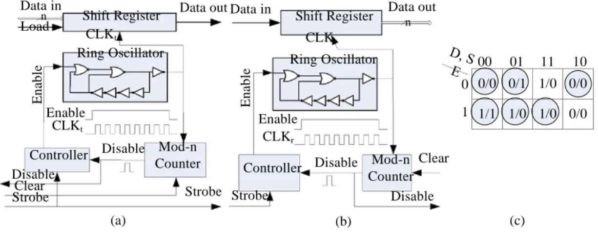
In the transmitter (cf. Figure 1(a)), a ring oscillator is used to generate a serial transfer clock
to synchronize the serial transmission of the data. This ring oscillator starts its oscillation after the rising
or falling edge of the strobe and generates the transmitter clock, CLKt. Next, the data is sent on the link
by shifting out the content of a shift register by CLKt (a parallel-to-serial converter). Therefore, the
edge of the first bit of data in the transmitter occurs after the edge of the strobe. Since the lengths of the
data and the strobe lines are approximately the same, the data and the strobe signals will have
nearly equal propagation delays on the links between the two cores. Therefore, the strobe signal reaches
the receiver m receiver ring oscillator, which subsequently generates the receiver clock, CLKr. If the
receiver clock generator is the same as the transmitter clock generator, then the edge of the first bit
of data in the receiver and the rising edge of CLKr shall roughly occur at the same time whereas, for
proper sampling of
received data, the falling edges of CLKr occur in the middle of the data bit
duration.
Data in
n
Load Shift Register
Data out Data in
CLKt Ring Oscillator Shift Register CLKr Ring Oscillator Data out n
00 01 11 10
0 Enable CLKt Controller Disable Clear
Disable Mod-n Counter
Strobe
Enable CLKr
Controller Disable Mod-n Counter 1 Clear Strobe (a) Strobe (b) Disable (c)
Figure 1 a) Block diagrams of the SSS transmitter b) Block diagrams of the SSS receiver c) Transition
table of the controller. D: disable input, S: strobe input, E: enable output.
The transmitter and the receiver require a controller and a binary counter to generate the proper signal
by the ring oscillator and when the desired number of clock cycles are generated, it clears the output of
the controller (disables the ring oscillator). The controller sets its output (enable signal) to ‘1’ at both the
rising and the falling edges of the strobe input and resets its output to ‘0’ at the rising edge of the disable
input. The controller, whose transition table is depicted in Figure 1(c), does nothing at the falling edge of
the disable input. On the transmitter side, before transmission of an n-bit frame, the block that generates
the frame also produces a clear pulse (on the Clear line of the transmitter) when the frame is ready. This
pulse resets the transmitter counter to prepare it for the data frame transmission. Similarly, on the receiver
side, after reception of an n-bit frame, the block that consumes the received frame also produces a clear
pulse (on the Clear line of the receiver) when it has registered the received frame. This resets the receiver
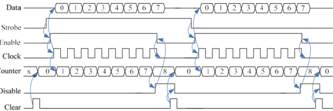
counter to make it ready for a new frame reception. The complete waveforms of the transmitter side of the
SSS scheme have shown in Figure 2. As is evident from the figure, the data is transferred on the data
line after the strobe signal’s rising or falling edge. As mentioned earlier, the strobe signal reaches the
receiver earlier than the data by an amount equal to tstrobe →data . The strobe signal enables the clock
generator at the receiver and a shift register samples the data line at every clock of the receiver
clock generator (CLKr). If the receiver clock generator is the same as the transmitter clock generator,
the frequencies of CLKr and CLKt are equal. Referring to Figure 1 and Figure 2, we may write
t strobe →data ( rec ) = t strobe →enable + t enable →clk + t clk →data + t line
(1)
t strobe →clk ( rec ) = tline + t strobe →enable + t enable → clk
(2)
Δt = t strobe →data ( rec ) −t strobe →clk ( rec ) = t clk → data
(3)
where
tstrobe→data(rec) denotes the delay from the edge of Strobe at the transmitter to the start of the first data
bit time at the receiver,
tstrobe→enable is the delay from the edge of Strobe to the edge of Enable in the Controller (Figure 1(a)),
tenable→clk denotes the delay from the edge of Enable to the edge of the first clock of Ring Oscillator,
tclk→data is the delay from the edge of the first clock to the start of the first data bit time in Figure 1(a)
(Shift Register),
tline corresponds to the delay of the data and the Strobe interconnect lines, and finally,
tstrobe→clk is the delay from the edge of Strobe at the transmitter to the edge of the first clock at the
Notice that we add a delay (equal to ∆t or tclk→data) on the Strobe to the Clkr path in the receiver (for
example in the output of controller) to adjust the rising edge of the first pulse of Clkr on the start of the
first data bit time at the receiver. Therefore, the falling edges of the Clkr, which occur in the middle of the
data bit duration, must be used as the falling edge of the clock for sampling the data line in the receiver.
After receiving a complete frame of the data, the disable signal is asserted to stop the ring
oscillator. Finally, the output port reads the data from the receiver shift register, activates the clear
signal, and
prepares the receiver for receiving the next data frame.
Figure 2. Timing waveforms for various data and control signals for the proposed SSS scheme
(transmitter side).
III.
The Single Wire Serial (SWS) Interface
In this section, we describe the proposed in-band Single Wire Serial interface (SWS) scheme for serial
communication between two cores. The scheme makes use of only one line for communicating both data
and control signals between the two cores. Every frame of data (containing control signals) has (n + 2)
bits, including a start-bit (‘1’), n bits of data, and a stop-bit (‘0’), which are transferred serially on the
serial line. Every data frame is started with the start bit, which plays the role of the strobe signal
for initiating the sampling of the data at the receiver.
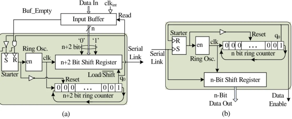
The transmitter reads n-bit data words from an input buffer and then makes the (n + 2) bit frame by
adding the start and the stop bits at the start and the end of the data word, respectively. Each frame is
transferred on the serial line (Data Line) by shifting right the bits in (n + 2) consecutive clock cycles of
the transmitter ring oscillator. When the positive edge of the start bit is detected by the receiving core, a
ring oscillator in the receiver is enabled to generate the receiver clock. Then the serial line is sampled at
disabled. Therefore, the n bits of the data (without the start and the stop bits) are sampled and stored in an
output buffer. Two separate ring oscillators, whose circuits are the same, generate the clocks for
the transmitter and the receiver. Hence, the frequencies of the clocks should theoretically be the same.
The same ring oscillator as shown in Figure 1 is used here.
A. Transmitter
The operation of the transmitter, whose block diagram is shown in Figure 3(a), is initiated by using a
starter (RS flip-flop) when some data words are ready in the input buffer and is stopped when the last data
word is transmitted and the input buffer has become empty. Before any transmission, the output of the
starter is zero, the ring oscillator is disabled, and (n + 2) bit ring counter is in the reset state. Thus, only
the LSB output of the ring counter (q0) is ‘1’. When the first data-word is loaded in the input buffer, the
output of the starter becomes active thereby enabling the ring oscillator. At the positive edge of the first
clock, an (n + 2) bit data frame will be loaded in the transmitter shift register. Then, in the next (n + 1)
clocks, the transmitter shift register shifts out the data frame bit by bit. The ring counter rotates right too.
After (n + 2) clock cycles, the stop bit is transferred on the serial line and q0 will become ‘1’. At this
time, if the input buffer is empty, the ring oscillator will be disabled and the serial line will go into the
zero state (the parking mode). Otherwise, the next data word will be read from the input buffer and loaded
into the shift register at the next positive edge of the clock. Therefore, the data transmission of an n-bit
real data in n + 2 clock cycles continues without any interruption.
Buf_Empty
Data In clkint
Input Buffer n
Read
Starter Reset q
0
Ring Osc. n+2
‘0’
bit ‘1’ Serial R
Serial S
en clk 0 0 0 . . . 0 0 1 n bit ring counter
S R en clk n+2 Bit Shift Register Link Link Ring Osc.
Starter
Reset Load/Shift q0 n-Bit Shift Register
0 0 0 . . . 0 0 1
n+2 bit ring counter n-Bit
Data Out
Data Enable
(a) (b)
B. Receiver
The operation of the in-band SWS serial receiver, whose block diagram is depicted in Figure 3(b), is
initiated using a starter (RS flip-flop) when a low-to-high (low is due to the stop bit of the previous frame
and high is from the start bit of the current frame) transition occurs on the input serial line. After being
enabled, the receiver reads an n-bit data word from the input line during the next n consecutive clocks.
The starter is reset before receiving a new data frame. Before the first low-to-high transition on the input
serial line, the output of the starter is zero, the ring oscillator is disabled, and the n-bit ring counter is in
the reset state while only q0 is ‘1’. The first low-to-high transition on the input serial line changes the
starter output to the high state, thereby enabling the receiver ring oscillator. Subsequently, in the next n
consecutive clocks, the receiver shift register is shifted right bit by bit receiving the data from the input
serial line while the ring counter rotates right. Therefore, after n clock cycles, a complete n-bit data word
will be ready on the parallel output data lines while the LSB output of ring counter (q0) will become ‘1’.
Finally, the starter is reset, thereby disabling the receiver ring counter and the n-bit parallel data is loaded
into an output buffer. At this time, the receiver becomes ready for receiving the next start of frame (low-
to-high transition on the input serial line).
IV.
Parallel SSS and SWS Interfaces
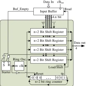
The proposed SSS and SWS schemes may be utilized in parallel communication or wider link schemes
between cores in NoC’s. For this purpose, we only need to use several shift registers in the transmitter
with the same control circuits. In the destination, every serial line must have a separate receiver
to eliminate jitter and mismatch between the parallel lines. In this case, the received data will be valid
when all the Data Enable signals in the receivers become active. The block diagram of a 4-bit
transmitter with the SWS scheme is shown in Figure 4 where we load the LSB of all shift registers
with ‘1’ (start bit).
Similarly, one can extend the serial SSS transceiver to the parallel SSS one.
Data In clkint
Buf_Empty
Input Buffer 4.n bit
Read
‘0’ ‘1’
n+2 Bit Shift Register
n+2 Bit Shift Register
n+2 Bit Shift Register
Data out 4
Ring Osc. S R en clk
n+2 Bit Shift Register
Load/Shift
Starter Reset q0
0 0 0 . . . 0 0 1 n+2 bit ring counter
Figure 4. The block diagram of the proposed SWS scheme for a 4-bit parallel bus.
V.
Tolerance to Frequency Difference between the Receiver and the Transmitter
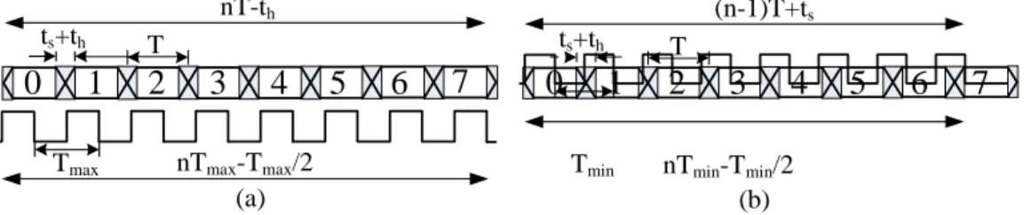
Inthe SSS structure, we add a small delay in the clock path of the receiver shift register to adjust the first
negative edge of the receiver clock in the middle of the first data bit time. Next, we must ensure that the
edge of the last receiver clock does not occur in the failure zone. Figure 5 shows these conditions where
in Figure 5(a) (Figure 5(b)), the frequency of the receiver ring oscillator is lower (higher) than
the frequency of the transmitter ring oscillator. In both of these cases, all the negative edges of the
receiver clock cycles are in the proper region. In this figure, ts and th are the setup and hold times of
the receiver
shift register. The same figures may be used for the SWS scheme, except that in this case we adjust the
first positive edge of the receiver clock in the middle of the first data bit time. Referring to the figure, the
condition for error free sampling in the receiver may be expressed as
n.T −t h >
(n
− 1 2)
.Tmax(n
− 1)T
+ t s <(n
− 1 2)T
min(4)
(5)
where n is number of bits per frame. Using these inequalities, one may write
fr,min < fr < fr,max (6)
(
n − 1 2)
.f tf r ,min =
n −th .f t (7)
(
n −1 2)
.f t (8)f r ,max =
n −1 + ts .f t
Here, ft (= 1/T) and fr are the clock frequencies of the transmitter and the receiver, respectively.
These equations show in our schemes we can have some frequency mismatching between
transmitter and receiver. The maximum acceptable mismatching is depended to the length of frames (n)
and we can have
higher mismatching for smaller value of n.
ts+th
nT-th
T ts+th
(n-1)T+ts
0
1
2
3
4 5
6
7
T
0
1
2
3
4 5
6
7
Tmax nTmax-Tmax/2 (a)
Tmin nTmin-Tmin/2 (b)
Figure 5 Timing diagram of the receiver. (a) The receiver ring oscillator is slower than the transmitter
ring oscillator. (b) The receiver ring oscillator is faster than transmitter ring oscillator.
VI.
Power Dissipation Analysis
The total interconnect capacitance per unit length Ct can be modeled as [13][14]
C t =
(
αC g + (MCF l + MCF r)
.C c)
(9)where Cg is the line-to-ground capacitance per unit length and Cc is the coupling capacitance per
unit length between two neighboring lines. The switching factor of Cg, that is α, is 1 for the top
layer interconnects and 2 for the intermediate layer interconnects because there are two metal layers
above and below any line of the intermediate layer interconnects. Assuming each interconnect is only
coupled to its nearest neighbors, MCFl and MCFr are the Miller coupling factor between the line of
interest and its left and right neighboring lines and it depends on their relative switching activity as
stated here. The factor is
2, 1, and 0 for two oppositely switching neighboring lines, only one line switching while the other
is quiet, and for two similarly switching neighboring lines, respectively. If the transitions are
uniformly distributed MCFav = 1 [13]. Hence, the average energy dissipation per unit length of an
E = 0.5C V
DD
2
av t ,av DD (10)
where Ct,av is the average capacitance and VDD is the supply voltage.
The line-to-ground and the coupling capacitance per unit length of an interconnect line on a ground
plane or top layer interconnect can be modeled by Equations (1) and (2) of [15] while the resistance and
the inductance per unit length of an interconnect line have been modeled in [14]. The ITRS projections of
the interconnects for different technologies may be found in [16]. Using the results presented in these
references, we can calculate the parasitic capacitances, resistance, and inductance of interconnect lines.
The result of these calculations show that the total interconnects capacitance per unit length (Ct) does not
decrease while the average length of global interconnects increases with process technology scaling.
Therefore, the power consumption of interconnections increases with the technology scaling. In contrast,
power consumption per logic gate decreases with technology scaling.
In the SSS scheme, we reduce the switching activity on the control line, resulting in a
significant improvement in the interconnect energy dissipation while in the SWS scheme, we reduce the
number of bus lines from two to one. Therefore, for the same bus area, the reduction in the number of
bus lines can lead to larger interconnect space (and/or width). Larger interconnect space reduce
the coupling capacitance, while wider interconnects reduce the line resistivity, leading to a significant
improvement in the interconnect energy dissipation and delay. The reduction in the delay can be
transformed into a further energy savings by reducing the number and size of the required repeaters. This
improvement increases as the technology scales.
Using a distributed model for top layer interconnects (we assume that the top layer is used for inter-
core communication lines), the energy dissipation per transition per unit length of any interconnect can be
calculated by Equations (9) and (10) with α = 1 and MCFl = MCFr = 1. Therefore, the energy
dissipation
per unit length in the SSS and SWS serial link per a frame of data may be expressed as
Eav,SSS = 0.5(Cg + 2.Cc ).V
2
(SAdata + SAstrobe) (11)
In this equation, Cg2 and Cc2 are the line-to-ground and coupling capacitance per unit length of an interconnect layer on a ground plane in a SWS serial link, respectively. One can show that for 8-bit random data frames, the average switching activity (SA) value of a SWS scheme is 5.5 while the sum of the average values of the data and control (strobe) switching activities (SAdata + SAcontrol) in three
different
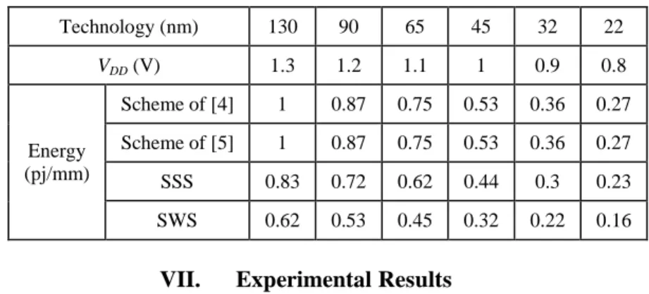
2-wire serial links, namely, scheme of [4], scheme of [5], and SSS schemes are 6, 6, and 5, respectively. The parasitic capacitances of SWS scheme calculated from [15] are presented in Table I. The normalized
energy dissipation per unit length per 8-bit random data frame transmission for four different serial link schemes are reported in
Table II. These results show that the SSS and SWS schemes are more efficient than the schemes of [4]
and [5].
Table I. Parasitic capacitance of SWS interconnect.
Technology (nm) 130 90 65 45 32 22
Cc 45 46 48 41 36 34
Cg 45 43 42 34 29 25
Ct = Cg + 2.Cc 135 135 138 116 101 93
Table II. Comparison of normalized energy dissipation per unit length per 8-bit data frame transmission.
Technology (nm) 130 90 65 45 32 22
VDD (V) 1.3 1.2 1.1 1 0.9 0.8
Energy (pj/mm)
Scheme of [4] 1 0.87 0.75 0.53 0.36 0.27
Scheme of [5] 1 0.87 0.75 0.53 0.36 0.27
SSS 0.83 0.72 0.62 0.44 0.3 0.23
SWS 0.62 0.53 0.45 0.32 0.22 0.16
VII.
Experimental Results
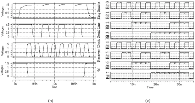
To evaluate the performance of the SSS and the SWS transceivers, the complete circuits shown in Figure
1 and Figure 3 were simulated at the transistor level (with HSpice) by using a 0.13µm standard CMOS
technology [14]. The simulations were performed for serial and 4-bit parallel buses for 8-bit frames. Fig.
6(a) shows the waveforms of the data, the strobe, the clock, and the enable of the ring oscillator at the
receiver of the SSS serial bus. In this figure, the receiver reads the sequence of “10101010”. The
results show that the transmitter and the receiver can operate up to a clock frequency of 4.05GHz.
In eight successive clocks, the 8-bit input shift register shifts right bit-by-bit to read the received data
from the serial input line while in the ninth clock cycle, the received data is loaded into the receiver
buffer. Next, the receiver can start a new reception of data. When the receiver is reading new data from
the serial line, the previous received data can be transferred into the next stage without any
1.8GBps.
To evaluate the performance of the SWS transceiver, we use an input (output) buffer with 16 8-bit
registers. Fig. 6(b) shows the HSpice simulation results for the waveforms of the enable signal of the ring
oscillator (Ring Enable), the Serial Line, the clock (Receiver Clock), and the LSB of the ring counter (q0)
at the receiver for one data frame of “01010101”. The results show that the transmitter and the receiver
can operate with a clock frequency up to 5.36GHz. The effective data transmission rate (excluding stop
and start bits) is about 4.288Gbps, which is equivalent to 536MBps per serial line. In another simulation,
we loaded the input buffer with 16 data words as 11h, 22h, 33h, 44h, … FFh, and 00h, and transmitted
these data words serially. The receiver block received these data and stored them in the output buffer. Fig.
6(c) shows the output waveforms of the output buffer (8-bit parallel outputs) where the transmission
frequency of 4.8 GHz was used.
(b) (c)
Fig. 6 a) waveforms of the SSS transmitter b) waveforms of the SWS transmitter c) Output waveforms of
the receiver buffer in the SWS scheme.
To assess the effect of the number of bits per frame (N) to the amount of the tolerable frequency
mismatch between the transmitter and receiver, we used Equations (7) and (8) to obtain the minimum
and maximum frequencies of the receiver assuming ts and th to be both equal to zero. The results, which
are reported in Table III, show that as the number of bits increases, the receiver frequency tolerance
decreases.
Table IV shows the permissible range of the receiver frequency calculated using Equations (7) and (8)
as well as simulations for the case where the transmitter frequency (ft) were 4Ghz and 1.8GHz. Note
that simulations of the designs used in this study led to the set-up time (ts) and hold time (th) of 60 and
50ps, respectively. The simulation results given in the table show that we can have about ±3.8% and
±6.1% tolerances in the receiver frequency, respectively.
Table III. The permissible range of the receiver frequency.
N 4 8 9 10
fr,min 0.875 0.938 0.945 0.95
fr,max 1.166 1.071 1.0631.055
ft (GHz)
fr (max) fr (min)
Calculated Simulated Calculated Simulated
1.8 1.9 1.91 1.71 1.68
4 4.17 4.19 3.87 3.85
We also simulated the two schemes that have been proposed in [4] and [5] at the transistor level by
using the same 0.13 µm standard CMOS technology and compared them with our schemes. Table
V which shows the number of transistors, maximum frequency and bandwidth for implementing
the different communication schemes reveals that the transistor count for the SSS (SWS) scheme is
7% (11%) and 8% (9%) lower (more) than those of schemes in [4] and [5], respectively. The
maximum bandwidths of SSS (SWS) is 32% (55%) and 23% (45%) faster than the schemes of
[4] and [5], respectively.
Table V. Complexity and performance of different schemes.
Number of transistor Performance (GHz, MBps)
Transmitter Receiver Total Maximum
Frequency
Maximum
Bandwidth
Scheme of [4] 252 174 426 3.22 345
Scheme of [5] 285 146 431 3.41 370
SSS Scheme 206 190 396 4.05 435
SWS Scheme 257 214 471 5.36 536
We calculated the power consumptions of different schemes at 345MBps, which all of the schemes
can operate at for different lengths of interconnect (without any repeaters) by HSpice.
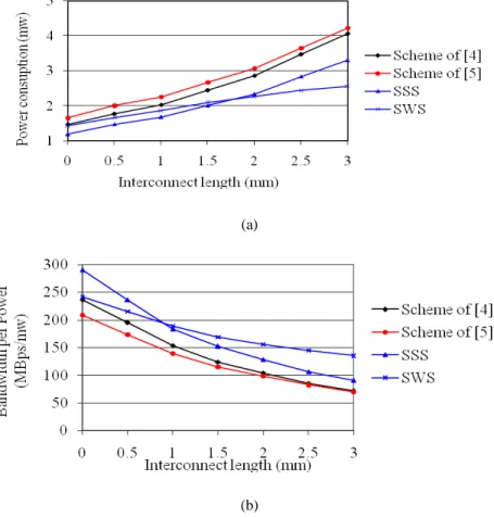
Experimental results are shown in Figure 7(a). These results show that although the SSS scheme
consumes more power than the schemes of [4] and [5] at the maximum frequency (or bandwidth), but
for the same bandwidth it consumes less power. The lower power consumption is expected due to the
lower switching activity on the strobe line of the SSS scheme. As Figure 7(a) reveals, the power
consumption of the SWS scheme is much lower than those of other schemes especially for longer
interconnects. For an interconnect with the length of 3mm, at the bandwidth of 345MBps, the power
consumption of the SWS (SSS) scheme is about
Figure 7(b) shows the bandwidths per unit power consumption of different transceivers at 345MBps.
This figure shows that the bandwidth of the SSS scheme at 345MBps is 21% (23%) and 35% (28%)
more than those of schemes in [4] and [5], respectively, for 1mm (3mm) interconnect layers. The
bandwidth improvement of SWS scheme relative to the schemes of [4] and [5] for 1mm (3mm)
interconnect layers is
9% (59%) and 21% (65%), respectively. This figure shows that for interconnects longer than 1mm, the
SWS scheme is the best communication scheme while for interconnects shorter than 1mm, the
SSS scheme is the best one.
(a)
(b)
Figure 7 a) Power consumption at 345MBps b) Bandwidth per power consumption for different schemes
at 345MBps.
VIII.
Conclusion
In this paper, two serial communication schemes for the communication over serial buses in a network on
chip were presented. The techniques, called SSS and SWS, removed the metastability errors in
the mesochronous communications. In both methods, the transmitter and the receiver had separate
tolerable frequency differences. In the first method, a strobe line was used to activate the
oscillators. Local counters were used to count the number of bits in the data frame and to stop the
local oscillators when the frame is processed. In the second method, a single physical line was used to
transmit both data and control information. The data transmission was controlled by the output of a
flip-flop, indicating the empty/full state of an input buffer whereas the data reception is controlled by
decoding a ‘1” start bit and a ‘0’ end bit which have been added to the n-bit data word to form a frame.
Both schemes can be used for parallel buses without any change in the control circuits. Results of
HSpice simulations in a 0.13µm standard CMOS technology showed that the maximum bandwidths
of the schemes were considerably higher than those of the previously proposed techniques in the
literature. These techniques also showed considerable power savings especially as the interconnect
lengths are increased. Our simulation results showed that the maximum bandwidth of SSS and SWS
schemes were 3.6Gbps and 4.288Gbps that were
32% (23%) and 55% (45%) higher than the scheme of [4] ([5]). For 3mm interconnects, at
345MBps bandwidth, the power saving in the SWS and SSS schemes were 37% (39%) and 19% (22%)
relative to scheme of [4] ([5]).
Acknowledgement
Mohsen Saneei and Ali Afzali-Kusha acknowledge the financial support by the Iranian National
Science Foundation.
References
[1] International Technology Roadmap for Semiconductors (ITRS 2003)
[2] D. Bertozzi and L. Benini, “Xpipes: A Network-on-Chip Architecture for Gigascale
Systems-on- Chip,” IEEE Circuit and Systems Magazine, Second Quarter 2004, pp.18-31.
[3] L. Benini and G. De Micheli, “Network on Chips: A New SoC Paradigm,” IEEE Computer, Jan.
2002.
[4] S. Kimura, T. Hayakawa, T. Horiyama, M. Nakanishi, and K. Watanabe, “An On-Chip High Speed
Serial Communication Method Based on Independent Ring Oscillators,” in the Proceedings of The
[5] I. C. Wey, L. H. Chang, Y. G. Chen, S. H. Chang, and A. Y. Wu, “A 2Gb/s High-Speed Scalable
Shift-Register Based On-Chip Serial Communication Design for SoC Applications,” in
the Proceedings of The IEEE International Symposium on Circuits and Systems, ISCAS 2005,
23-26
May 2005, Vol. 2, pp.1074 – 1077.
[6] H. Kaul, and D. Sylvester, “Low-Power On-Chip Communication Based on Transition-Aware Global
Signaling (TAGS),” IEEE Transaction on Very Larg Scale Integration (VLSI) Systems, Vol. 12, No.
5, May 2004, pp. 464-476.
[7] E. Beigné, F. Clermidy, P. Vivet, A. Clouard, and M. Renaudin, “An Asynchronous NOC
Architecture Providing Low Latency Service and its Multi-level Design Framework,” in the
Proceedings of The 11th IEEE International Symposium on Asynchronous Circuits and
Systems (ASYNC’05), 2005.
[8] J. Teifel and R. Manohar, “A High-Speed Clockless Serial Link Transceiver,” in the Proceedings of
The 11th IEEE International Symposium on Asynchronous Circuits and Systems (ASYNC’03), 2003,
pp. 151-161.
[9] F. Mu and C. Svensson, “Self-Tested Self-Synchronization Circuit for Mesochronous Clocking,”
IEEE Transaction on Circuits and Systems, vol. 48, no. 2, Feb. 2001, pp. 129-140.
[10] I. Söderquist, “Globally Updated Mesochronous Design Style,” IEEE Journal of Solid-State
Circuits, vol. 38, no. 7, July 2003, pp. 1242-1249.
[11] B. Mesgarzadeh, C. Sevensson, and A. Alvandpour, “A New Mesochronous Clocking Scheme for
Synchronization in SoC,” in the Proceedings of The IEEE Int. Symposium ond Circuit and Systems
(ISCAS04), 23-26 May 2004, vol. 2, pp. II - 605-608.
[12] S. J. Lee, K. Kim, H. Kim, N. Cho, and H. J. Yoo, “Adaptive Network-on-Chip with Wave-Front
Train Serialization Scheme,” in the proceding of Symposium on VLSI Circuits Digest of Technical
Papers, 2005, pp.104-107.
[13] M. Ghoneima, Y. Ismail, M. Khellah, J. Tschanz, and Vivek De, “Serial-Link Bus: A Low-Power
On-Chip Bus Architecture,” in the proceding of International Conference on Computer-Aided
Design, ICCAD-2005. Nov. 6-10, 2005, pp. 541 - 546.
[15] S-C. Wong, G-Y. Lee, D-Y. Ma, “Modeling of Interconnect Capacitance, delay and crosstalk in
VLSI,” IEEE Transaction on Semiconductor Manufacturing, vol. 13, no. 1, Feb. 2000, pp. 108-111.
[16] S. Im, N. Srivastava, K. Banerjee, and K. E. Goodson, “Scaling Analysis of Multilevel Interconnect
Temperatures for High-Performance ICs,” IEEE Transactions on Electron Devices, vol. 52, no. 12,