Eman M. Noori
X-Ray Techniques Department, Institute of Medical Technology, Middle Technical University, IRAQ.
A r t i c l e I n f o
ABSTRACT
Received
10/2/2016
Accepted
8/5/2016
Cadmium (Cd) and selenide powder used to prepared cadmium selenide alloy. (CdSe) thin films of thickness 1320 Å were thermally evaporated technique deposited on glass substrate at room temperature. The as-deposited films were annealed in air atmosphere at 100oC, for three different annealing times (60, 120 and 180 minutes). The structural investigation performed by x-ray diffraction (XRD) technique; showed that the films have a polycrystalline and hexagonal (wurtzite) structure. For all deposited films the preferential orientation is (002).The value of lattice constant (a), grain size, strain and dislocation density of the deposited films are calculated and their variations with annealing times are studied. The absorbance spectra of cadmium selenide thin films were recorded in the wave length range of 400 nm to 900 nm. The values of the optical band gap energy, Eg (allowed direct transitions), calculated from the
absorption spectra, ranged between (2.54 and 2.41) eV.
Keywords: Structure properties, Optical properties, Annealing time, Cadmium Selenide
(CdSe)
1320 Å 373 K
(XRD) (022)
(a)
400nm 900nm
Eg
2.54 ) 2.41
eV
:
INTRODUCTION
Cadmium selenide (CdSe) is one of the most investigated A BvI semiconductor materials.
Specific physical characteristics of this compound make it very attractive for various applications, in particular as solar cells, high-efficiency thin-film transistors, etc. [1-7]. A study of the correlation between physical properties of the CdSe films and their annealing time is still necessary for more
comprehensive understanding of this
correlation and for the improvement of the quality of these films for the technological. Several methods of preparation of CdSe films have been reported in various literatures in recent years [8-13].
A thorough study of various aspects of the film is important for application of CdSe in device fabrication. In this paper the influence of annealing time on the structural and optical properties of CdSe thin films are investigated. In the structural parameters the lattice constant, a, and, c, for hexagonal crystals are evaluated from the following relation [14]
The grain size (D) for the thermally evaporated CdSe thin films are evaluated using Scherrer formula [15].
wavelength of the
x-wavelength full width at half maximum value
's angle.
by using Equation [16].
the crystallite size of samples using Williamson and Smallman's formula [17].
The dependence of the absorption coefficient on the incident photon energy (h ) can be written as [18].
Where A is constant, n=1/2 for direct allowed transition, Eg is optical band gap energy of the
material.
EXPERAMENTALE
Quartz tube was filled with Cd and Se grains at equal molar proportion. The purity of the materials is 99.999%. The quartz ampoule was linked by specific design to the vacuum unit. When the pressure reached 1x10⁻³ mbar the
ampoule was sealed. The evacuated ampoule was placed in an electric furnace that was heated slowly to 1173 K and kept in this temperature for seven hours. In the reverse way, the furnace temperature was reduced to room temperature at which the ampoule was removed from the furnace and was broken safely. This alloy was used to prepare CdSe thin films by thermal evaporation. The chamber was evacuated to pressure of 10
-5Toor. The substrate temperature was kept at
room temperature and the source substrate distance was kept at 30 cm.The films have
been deposited on ultrasonically and
chemically cleaned glass substrates. The thickness of the deposited films was 1320 Å. The thin films samples annealed at 373 K for different period of time (0-180 minutes). The structure analysis of alloy and films was performed by x-ray diffraction (XRD)
wavelength 1.54056 Å. It was operated with a target voltage and current of 30kV and 20 mA, respectively. The diffraction patterns were
o o
The optical transmission spectra of the prepared samples were recorded, at room temperature, by UV-Vis Unicom double from 400-900 nm.
RESULTS AND DISCUSSION
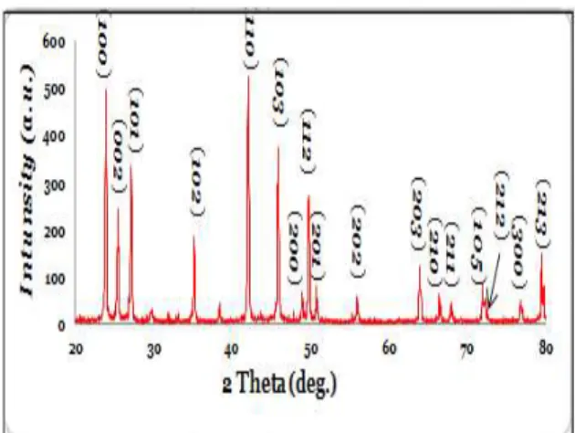
Figure 1 X-ray diffractometer (XRD- 600, Shimadzu, X ray diffractometer) with Cu K
was utilized to investigate the structural properties of CdSe thin films. Also Figure 1 show that all the synthesized CdSe thin films are hexagonal structure according to JCPPS file No: 8-459[19].
A shift in the diffracted peaks related to (100) and (103) planes was observed at 23.930, 42.050 and 45.850 respectively. Some
Figure 1: XRD patterns for as-prepared CdSe powder.
Table1: Structural parameters of as-prepared CdSe powder.
(deg)
Lattice spacing
d (Å) I/IO Plan (hkl)
Lattice constant
a(Å)
Lattice constant
c(Å)
23.93 3.71 80 100 4.28 7.00
25.45 3.49 36 002 4.28 6.99
27.14 3.28 55 101 4.29 7.00
35.17 2.54 33 102 4.29 7.00
42.05 2.14 100 110 4.29 7.01
45.85 1.97 75 103 4.29 7.00
48.92 1.86 11 200 4.29 7.01
49.75 1.83 54 112 4.29 7.01
50.74 1.79 14 201 4.29 7.01
55.91 1.64 11 202 4.29 7.01
63.90 1.45 25 203 4.29 7.01
66.41 1.40 11 210 4.29 7.01
67.90 1.37 8 211 4.29 7.01
71.93 1.31 15 105 4.29 7.00
72.30 1.30 9 212 4.29 7.01
76.76 1.24 9 300 4.29 7.01
79.46 1.20 28 213 4.29 7.01
Figure 2: XRD patterns for CdSe films annealing at 273 K for different annealing times.
Once the structure is confirmed, the lattice constant (a) of hexagonal phase of the CdSe thin films deposited in the present work were evaluated using the Equation (1). This value is presented in Table (2).The lattice constant for each CdSe thin films annealed at 373 K for period time (0-180) min. was found nearly equal i.e. 4.294 to 4.2992 Å. The observed lattice constant, in present, study was in agreement with the result 4.292 Å as reported by other worker [21] and standard value of 4.299 Å [JCPDS 8-459].
The crystallite size of CdSe thin film was calculated using XRD analysis and using Scherrer formula Equation (2).
As can be seen in Table 2, an increasing annealing time also, influences the crystal size of CdSe films. It was due to increase of growth of crystallite with increase of annealing time. The microstrain in thin film is defined as the miss arrangement of lattice created during the deposition and depends upon the deposition parameters. In present study for (002) plane, the strain was decreased (14.80 to 12.54) x 10-4 (line-2 m-4) with increase of annealing time. The lower strain 12.54 x 10⁻⁴ (line-2 m-4)was observed for film annealed time for 180 minutes which indicates better lattice arrangement.
Table 2: Calculated values of the structural parameters of CdSe thin films, having different annealing times.
Anneal Time
(min.) (deg.)
Lattice spacing
d (Å)
Plan (hkl)
Lattice constant
a(Å) FWHM (DEG.) D (Å)
-4
(line-2 m-2)
15
(line m-2)
0 25.36 3.50 002 4.29 0.34 247.46 14.80 1.67
45.81 1.97 103 4.29 0.40 227.19 15.07 1.97
60 25.36 3.50 002 4.29 0.31 269.48 13.43 1.37
45.81 1.97 103 4.29 0.49 182.56 19.83 3.00
120 25.35 3.50 002 4.29 0.29 291.42 12.59 1.21
45.78 1.98 103 4.29 0.29 314.57 11.65 1.03
180 25.35 3.61 002 4.29 0.29 291.58 12.54 1.20
45.79 2.00 103 4.29 0.64 141.73 25.72 5.04
0 min.
(002)
(103)
120 min. (002)
(103)
60 min.
(002)
(103)
180 min. (002)
The dislocation density is imperfection in the crystal which is created during growth of the films. It was observed in present study for (002) plane that the dislocation density decrease (1.67 to 1.20) x 1015 (line m-2) with increase of annealing time of the films.
Some characteristics of XRD patterns for studied samples are listed in Table 2. From these Tables and Figure 2, it is quite apparent that the values of h,k,l and d-spacing have been matched with the JCPDS database no. 8-459,it was inferred that CdSe possesses hexagonal structure in present investigation.
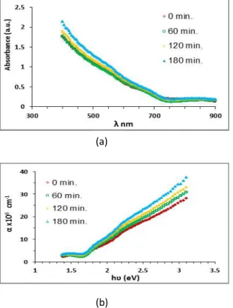
Figure 3 (a) shoes absorbance obtained for post- growth heat treatment of CdSe films at 273 K in air for different period of time (0-180) min. All the films show an increasing absorbance in the visible regain. Films annealed for 180 minutes have higher absorption values as compared with other films. This is due to the fact that film annealed time for180 minutes has the better crystallite reduces the reflectivity of incident photon on the surface and corresponding increases absorption due to multiple reflection.
Figure 3: (a) optical absorbance versus wavelength (b) Plot of photon energy dependence of absorption
coefficient for CdSe films annealing at 273 K for different annealing times.
The photon energy dependence of absorption coefficient is given in Figure 3(b).The dependence of the absorption coefficient on the incident photon energy (h ) can be evaluated from Equation (5).Figure 3(c) shows the plot ) 2 versus (h ) for CdSe thin film. The plot is linear depends, indicating a direct allowed transition. The straight line portion was extrapolated to the energy axis and when )2 = 0, the intercept gives the band gap energy of CdSe thin film [22]. The band gap values are greater than the bulk crystalline value (1.74 eV) [23]. It is known that such shift to higher energies of the optical band gap arise from very small grain and the resulting quantum confinement of electric states in thin films [24].Values of optical band gap energy for as-deposited CdSe thin film and annealed for period annealing time are shown in Table (3).
Figure 3: 2 versus photon energy gap of CdSe
films as a function of different annealing time.
Table 3: Values of optical band gap energy for different annealing time.
Annealed Time
(min.)
E
g(eV)
0
2.55
60
2.45
120
2.40
180
2.36
CONCLUSION
Cadmium selsnide alloy was successfully prepared. After deposited CdSe thin films on glass substrate, they annealed in air atmosphere at 373 K for 60,120 and 180 minutes and characterized for structure and optical properties. XRD analysis revealed that thin films exhibited polycrystalline and hexagonal structure. The films are found to have preferred orientation along (002) plane. Increase in optical absorption with annealing times resulted in lowering of the band gap value which will be advantageous for its use in photovoltaic cells.
REFERENCE
[1] Hankare P.P., Bhuse V.M., Garadkar
K.M., Delekar S.D., and Mulla I.S., Chemical deposition of cubic CdSe and
HgSe thin films and their
characterization, Semicond. Sci.
Technol., 19 (2004) 70-75.
[2] Harishchandra K. Sadekar, Anil
VithalGhule, Ramphal Sharma,
Fabrication of CdSe thin film for photosensor application, International Journal of Innovations in Engineering and Technology (IJIET), 5, Issue 1(2015)35-41,.
[3] Borah M.N., Chaliha S., Sarmah P.C., Rahman A., Electrical properties of
thermally evaporated doped and
undoped films of CdSe, Indian Journal of Pure&Applied Physics,45(2007) 687-691.
[4] Christopher E. Hamilton, Dennis J.
Flood and Andrew R. Barron,Thin film
CdSe/CuSe photovoltaic on a flexible
single walled carbon nanotube
substrate, Phys. Chem. Chem.
Phys.,15(2013) 3930-3938.
[5] Lou S., Zhou C., Wang H., Shen H., Cheng G.Du, Annealing effects on the
photoresponse properties of
CdSenanocrystal thin films, Mater. Chem. Phys., 128(2011)483-488.
[6] Murali K.R., Sivaramamoorthy K.,
Kottaisamy M., Asath S. Bahadur, Photoconductive studies on electron beam evaporated CdSe films, Physica B, 404(2009) 2449-2454.
[7] Saaminathan V., Murali K.R.,
Importance of pulse reversal effect of CdSe thin films for optoelectronic
devices, J. Cryst.Growth,
279(2005)229-240.
[8] CristianBaban, Rusu G.I., On the
structural and optical characteristics of CdSe thin films, Applied Surface Science, 211 (2003) 6-12
[9] Mathuri S., Ramamurthi K., Ramesh R.
Babu, Investigation on CdSe thin film deposited by electron beam evaporation technique, International Journal of Chem Tech Research,7,2, : 967-973,2015.
[10] Okereke N.A., and Ekpunopi A.J.,
Influence of thickness on the structure and optical properties of cadmium selenide thin films, Advances in Applied Science Research, 3, 3:1244-1249, 2012.
[11] Yadav A., Abhijit, Studies on cadmium
selenide (CdSe) thin films deposited by spray pyrolsipyrolysisials chemistry andphysics, 121(1-2)(2010)53-57. [12] Pogrebnjak A.D., Jamil N.Y., Abdulla
irradiation on the structural and physical properties of CdSe thin films,
Proceeding of the International
Conference Nanomaterials: Application and Properties, 2, 1,01PCSI21(2013) (3pp).
[13] Deshpande M.P., NityaGarg, Sandip V.
CdSe thin films deposited by chemical bath deposition, Advanced Materials Letters, ISSN 0976-3961: (2013) 1-13. [14] Sarmah K., SarmaR.,Das L., Structural
characterization of thermal evaporated CdSe thin films, Chalcogenide Letters 5,8,(2008)153-163.
[15] Klug H.P., and Alexander L.E., X-ray diffraction procedures: 491, John Willey and Sons Inc., New York, 1945.
[16] Williamson G.K., and Hall W.H., X-ray
line broadening from field aluminum and wolfram, Metallurgica, 1(1953) 22-31.
[17] Williamson G.K., and Smallman R.C., III, Dislocation densities in some annealed and cold-worked metals from measurement on the X-ray
debye-scherrer spectrum, Philosophical
Magazine (1956) 34-46.
[18] Zhao Y., Yan Z., Liu J., Wei A., Synthesis and characterization of CdSenanocrystalline thin film deposited by chemical bath deposited, Mater. Sci. Semicond. Process, 16(2013) 1592-1598.
[19] Powder Diffraction Data File, Joint Committee of Powder Diffraction Standard: 143 International Center for Diffraction Data, USA Card No.8-459, (1984)143.
[20] Patel K.D., Shah R.K., Makhija D.L., Pathak V.M., Srivastava R., Chemical and structural characterization CdSe thin films, Journal of Ovonic Research, 4,6(2008) 129-139.
[21] Klug H.P., and Alexander L.E., X-ray diffraction procedures: 491, John Willey and Sons Inc., New York, 1945. [22] Zhao Y., Yan Z., Liu J., Wei A., Synthesis and characterization of CdSenanocrystalline thin film deposited by chemical bath deposited, Mater. Sci. Semicond. Process, 16(2013) 1592-1598.
[23] Sze, S. M. Physics of semiconductor devices; 2nd Ed.: 848 John Wiley and Sons Inc.: New York, 1981.
[24] Moskovits M., In chemical physics of atomic and molecular clusters; Soles, G.