Design and Realization of FIR Filter for Inter Satellite Link at
50-90 MHZ Frequency using FPGA
Desain dan Realisasi Filter FIR untuk Inter Satellite Link
pada frekuensi 50-90 MHz menggunakan FPGA
Yuyu Wahyu
*,a, Ken Paramayudha
a, Lutfi Jamil Setiawan
b, Heroe Wijanto
b,
M. Shiddiq S. H.
c aPusat Penelitian Elektronika dan Telekomunikasi, Lembaga Ilmu Pengetahuan Indonesia. Komp LIPI Gd 20, Jl. Sangkuriang 21/54D, Bandung 40135, Indonesia
b
Program Studi Teknik Telekomunikasi, FakultasTeknik, Universitas Telkom Bandung, Indonesia
c
Sekolah Teknik Elektro dan Informatika, Institut Teknologi Bandung. Labtek VIII, Jalan Ganesha No. 10, Bandung 40132, Indonesia
Abstract
In this paper, design and realization of FIR filter with a bandwidth of 40 MHz at 50-90 MHz frequency has been proposed. The design was destined to be implemented on the Inter Satellite Links (ISL). This kind of filter had been selected due to a need in linear phase responseon the ISL data communication. Equiripple method was used to design the filter becauseof its reliability in minimizing the magnitude errors. The design of this FIR filter was conducted with theoretical calculation and simulation using the R2012b Matlab. For the implementation, FPGA was used with a VHDL as the programming language with a help of Xilinx ISE Design Suite 14.5. Simulation results in Matlab and Simulink indicated that the filter design could be well implemented on ISL at frequency of 50 MHz - 90 MHz with stopband of 60 db. The phase responseresult of the realized design is quite linear so that the filter is suitable for data communication on the ISL.
Keywords : FIR filter, equiripple, FPGA, VHDL.
Abstrak
Dalam tulisan ini, desain dan realisasi filter FIR dengan bandwidth 40 MHz pada frekuensi 50 - 90 MHz telah dibuat. Desain dimaksudkan untuk diterapkan pada Inter Satellite Link (ISL). Jenis filter FIR dipilih karena kebutuhan dalam respon fase linier pada komunikasi data ISL. Metode Equiripple digunakan untuk merancang filter karena kehandalan dalam meminimalisasi kesalahan. Metodologi desain filter FIR ini dimulai dengan perhitungan teoritis dan simulasi menggunakan R2012b Matlab. Untuk realisasinya, FPGA digunakan dengan VHDL sebagai bahasa pemrograman dan dengan bantuan software Xilinx ISE Design Suite 14,5. Hasil simulasi di Matlab dan Simulink menunjukkan bahwa desain filter dapat diimplementasikan pada ISL pada frekuensi 50 MHz - 90 MHz dengan stopband sebesar 60 db. Hasil respon fase pada realisasi cukup linear sehingga filter cocok digunakan untuk komunikasi data pada ISL.
Kata kunci : Filter FIR, equiripple, FPGA, VHDL.
I. INTRODUCTION
The satellite is an object that orbits around the earth that is normally used by humans as to communicated, weather monitoring, etc. The satellite technology continues to evolve. An Inter satellite links (ISL) is one of the technology that can make the satellites connect directly with other satellites.
The ISL is a solution of the existing problems on LEO satellites monitoring the earth. These satellites can only send a picture when the position above the earth station which causes the delay to get information. Therefore, the earth stations is made with large numbers in order to continue monitoring the LEO satellite. However, this requires a considerable high cost.
Because of that the ISL which can communicate the satellites directly with other satellites assessed more quickly and efficiently.
Filter is one of the components used in the ISL. The filter is used to pass the signals by passing frequency digital signal which contains the required info and reduce the undesired signal. In the recent years, many research of Finite Impulse Response (FIR) filters had been conducted. Some applications that could be implemented using this kind of filters are: image sampling [1], image coding [2], beamforming [3], software radio [4], audio [5], hearing aid [6] and DSP application [7]
In this paper, design and realization of FIR Filter with bandwidth of 40 MHz at 50-90 MHz frequency for ISL application are done. An Equiripple method was used to design the filter because of its reliability in minimizing the magnitude errors. The design of this FIR filter was conducted with theoretical calculations and simulated using Matlab R2012b. For the implementation, FPGA was used with VHDL as the
* Corresponding Author.
Email: [email protected]
Received:November 22, 2016; Revised: November 30, 2016 Accepted: December 2, 2016
Published: December 15, 2016
e-ISSN: 2527-9955 p-ISSN: 1411-8289
programming language and a help of Xilinx ISE Design Suite 14.5
II. FIRFILTER
A filter is one of the component in communication systems that is used to pass the desired frequency and stop unwanted frequency [8]. Band Pass Filter is one of the types of filters that has characters to allowed frequency in the range of a particular region (passband), and reduce the frequency area above and below the frequency range (stopband) [8].
The FIR filter is one type of filters which had a non recursive characteristic of the current output. It means that characteristic of the current output does not depend on the previous output, so it has a limited impulse response [8]. This makes the output of filter is calculated as the value of sum finite figures in the past, present, and possible future values of the input filter. Formulated in the Equation 1 [8] :
𝑦𝑦[𝑛𝑛] =� 𝑏𝑏𝑘𝑘𝑋𝑋[𝑛𝑛−𝑘𝑘]
𝑀𝑀
𝑘𝑘=0
= � ℎ(𝑘𝑘).𝑋𝑋[𝑛𝑛 − 𝑘𝑘
𝑀𝑀
𝑘𝑘=0
] (1)
FIR filterhas the following transfer function in Equation 2 [9] :
𝐻𝐻(𝑧𝑧) = 𝑌𝑌(𝑧𝑧)𝑋𝑋(𝑧𝑧)= ∑ 𝑏𝑏𝑘𝑘 𝑍𝑍−𝑘𝑘]
𝑀𝑀 𝑘𝑘=0
1 +∑𝑁𝑁𝑘𝑘=1𝑎𝑎𝑘𝑘 𝑍𝑍−𝑘𝑘] (2)
The impulse response of the ideal filter is showed in Equation 3[10]:
ℎ(𝑛𝑛) =2𝜋𝜋 �1 −𝑗𝑗𝜔𝜔1𝑒𝑒𝑗𝑗𝑗𝑗𝑛𝑛
−𝑗𝑗𝜔𝜔2 𝑑𝑑𝑗𝑗+� 𝑒𝑒
𝑗𝑗𝑗𝑗𝑛𝑛 𝑗𝑗𝜔𝜔2
𝑗𝑗𝜔𝜔1 𝑑𝑑𝑗𝑗
=𝜋𝜋𝑛𝑛1 sin(𝑗𝑗𝜔𝜔2𝑛𝑛)−𝜋𝜋𝑛𝑛1 sin(𝑗𝑗𝜔𝜔1𝑛𝑛)
ℎ(𝑛𝑛) =2𝜋𝜋 �1 −𝑗𝑗𝜔𝜔1𝑒𝑒𝑗𝑗𝑗𝑗𝑛𝑛
−𝑗𝑗𝜔𝜔2 𝑑𝑑𝑗𝑗+� 𝑒𝑒
𝑗𝑗𝑗𝑗𝑛𝑛 𝑗𝑗𝜔𝜔2
𝑗𝑗𝜔𝜔1 𝑑𝑑𝑗𝑗
=𝜋𝜋𝑛𝑛1 sin(𝑗𝑗𝜔𝜔2𝑛𝑛)−𝜋𝜋𝑛𝑛1 sin(𝑗𝑗𝜔𝜔1𝑛𝑛) (3)
The method of sampling frequency and windowing method is the simplest method to design an FIR filter. But both methods it’s also has a weakness in the lack of reliability to set the critical frequency as 𝑗𝑗𝑠𝑠 and 𝑗𝑗𝑝𝑝. Equiripple is a method that provides optimization in FIR filter design, to approach the magnitude of the error between the desired frequency response with the actual frequency response that spreads evenly on the passband and stopband so as to minimize the magnitude of the error.
The magnitude of the error can be formulated into Equation 4 [9]:
𝐸𝐸(𝑒𝑒𝑗𝑗𝑗𝑗) =𝑊𝑊�(𝑒𝑒𝑗𝑗𝑗𝑗)[𝐻𝐻�
𝑑𝑑𝑑𝑑(𝑒𝑒𝑗𝑗𝑗𝑗)− 𝑃𝑃(𝑒𝑒𝑗𝑗𝑗𝑗)] (4)
The weighting function and the desired frequency response is written in Equation 5 [2]:
𝑊𝑊�(𝑒𝑒𝑗𝑗𝑗𝑗) =𝑊𝑊(𝑒𝑒𝑗𝑗𝑗𝑗)Q(𝑒𝑒𝑗𝑗𝑗𝑗) (5)
𝐻𝐻�𝑑𝑑𝑑𝑑(𝑒𝑒𝑗𝑗𝑗𝑗) =𝐻𝐻𝑑𝑑𝑑𝑑�𝑒𝑒
𝑗𝑗𝑗𝑗�
Q�𝑒𝑒𝑗𝑗𝑗𝑗� (6)
From the error function
(
𝑒𝑒𝑗𝑗𝑗𝑗)
, the problem of Chebyshev approximation method (minimax) is to seek∝𝑘𝑘filter parameters that minimize the maximumerror of the band frequencydesired which can be formulated with in Equation 7 [9].
min𝑜𝑜𝑜𝑜𝑒𝑒𝑑𝑑{∝𝑘𝑘}�max𝑗𝑗∈𝑆𝑆�𝐸𝐸(𝑒𝑒𝑗𝑗𝑗𝑗)��
= min𝑜𝑜𝑜𝑜𝑒𝑒𝑑𝑑{∝𝑘𝑘}�max𝑗𝑗∈𝑆𝑆 �𝑊𝑊�(𝑒𝑒𝑗𝑗𝑗𝑗)[𝐻𝐻� 𝑑𝑑𝑑𝑑(𝑒𝑒𝑗𝑗𝑗𝑗)
− � ∝𝑘𝑘 𝐿𝐿
𝑘𝑘=0
cos𝑗𝑗𝑘𝑘]�� (7)
III. DESIGN AND SYSTEM REALIZATION The block diagram of a FIR filter design could be seen in Figure 1.
FILTER SPECIFICATION
FILTER DESIGN
SIMULATION
MATCH WITH SPEC?
SYNTHESIS
FPGA IMPLEMENTATION
MATCH WITH SPEC?
VHDL CORRECTION
TESTING
FINISH START
NO YES
NO
YES
Figure 1. Block Diagram of FIR Filter Design.
1) Matlab Design
The specification of FIR filter design :
• Stopband Frequency1 : 50 MHz
• Cutoff Frequency 1 : 52 MHz
• Cutoff Frequency 2 : 88 MHz
• Stopband Frequency 2 : 90 MHz
• Ripple : 0,1 dB
• Attenuation : 60 dB
• Sampling Frequency : 200MHz
In the matlab, there is a toolbox called FDA tool (Figure 2). This toolbox will help to design a filter.
FDA tool can show the magnitude response(Figure 3), the phase response (Figure 4) and the location of poles and zeros (Figure 5). It can prove whether the phase response of the filter is linear. The layout of the poles and zeros is to prove the stability of filter. Fir filter does not have a zero, because there is no feedback coefficient in it. FIR filter have a feed forward coefficient. This is why the FIR filter can be stabilized. If there is a pole in the loop, filter is stable, contrastly if a pole outside the circle then filter unstable. Total pole will be a number of filter coefficients.
Figure 5. Pole and Zero.
IV. SIMULATION AND ANALYSIS A. Matlab Analysis
In this scenario, Matlab simulation is conducted with a scale of 1 : 1.000.000. The block diagram of the simulation could be seen in Figure 6. In the simulation, FIR filter will pass a sinusoid signal with a frequency of 45 MHz, 50 MHz, 60 MHz, 65 MHz, 70 MHz, 75 MHz, 80 MHz, 85 MHz, 90 MHz, and 95 MHz. Sinusoid signals with these frequencies will then be passed to digital FIR filter that has been scaled to 1 : 1.000.000. Afterwards, the results could be obtained by plotting the filter output of sinusoid signal using Matlab.
SINUSOID SIGNAL
SCALLABLE DIGITAL FIR
FILTER
FILTER OUTPUT
Figure 6. Block Diagram of FIR Filter Simulation in Matlab.
Figure 7 represents the output of filtered signals at a frequency of 45 MHz. Input signal and output signal at a frequency of 55 MHz was depicted by Figure 8. The signal contained in the passband region will be passed. But there is a delay of 130 us before the signal can be read by the system. It is caused by a d elay element contained in the filter.
After a few experiment, magnitude response could be seen in Figure 9 while the phase response is illustrated in Figure 10.
Figure 9. Magnitude Response of FIR Filter.
Figure 10. Phase Response of FIR Filter
B. Simulink Analysis
Block Diagram of FIR Filter Simulation in Simulink was depicted in Figure 11. Two sinusoid input signals are generated. The sine signal from the DSP is signal information, while the random source is noise signal. The type of designed filter is a band stop filter which filters output signals originating from a random
Figure 3. Magnitude Response.
Figure 4. Phase Response.
Figure 7. Sinusoid Signal at Frequency 45 MHz.
e-ISSN: 2527-9955 p-ISSN: 1411-8289
source, so that the noise signal could not passed the system. Add block serves as a modulator to combine both the information signal and noise signal. Time scope in this block diagram serves to look at three things : Information signal, adder output signal before being filtered and the filter output signal.
A DSP sine wave frequency sinusoid signal issued by 45 MHz with amplitude equal to 1 could be seen in Figure 12. Random source will emit a signal indeterminate amplitude of 0 - 4 with a frequency between 0-50 MHz and > 90 MHz. The black line graph is sinusoidal signal that will be filtered. Purple line graph is a sinusoid signal that is passed filter. Blue line graph is information signal. The filter did not pass the sinusoid signal. Because the signal below 52 MHz frequency signal will be attenuated.
In Figure 13, it could be seen a DSP sine wave frequency sinusoidal signal issued by 55 MHz with an amplitude equal to 1. Random source will emit a signal indeterminate amplitude of 0 - 4 with a frequency between 0-50 MHz and > 90 MHz. The filter passed a sinusoid signal which has the same amplitude but also has a slightly different form. This is due to the delay of 130 μs in the FIR filter derived from the components
forming the FIR filter.
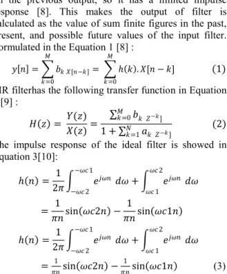
From the Table 1, we can concluded that the digital filter could be designed and implemented on the FPGA device, because FPGA resources utilization were below 100 % .
C. Designed Filter Performance Analysis
Block diagram scenario of implemented FIR filter on FPGA could be seen in Figure 14. FPGA ability to generate the signal was used in this scenario. The output digital FIR filter could be viewed using chipscope as
logic analyzer. Then the data will be collected and converted into decimal.
TABLE 1
FPGA RESOURCES FOR IMPLEMENTATION
Figure 14. Block Diagram of FIR Filter Implementation in FPGA.
FPGA ability to generate the signal was used in this scenario. The output digital FIR filter could be viewed using chipscope as logic analyzer. Then the data will be collected into a table and will be converted into decimal. Thus the output of the digital filter could be seen to builda magnitude response graphic. The data that taken from chipscope sampled 100 time. From these tests the output waveform obtained as seen in Figure 15. The output signal of the filter with a frequency of 30 MHz or below the pass band has a shape signal and did not pass sinusoid wave form. It was caused by the signal at that frequency attenuated by the system so it made the shape signal becomes damaged.
Figure 15. Output Signal at Frequency 30 MHz.
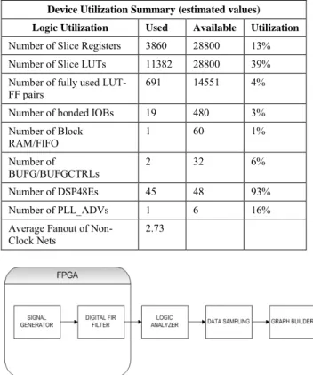
In Figure 16, the output signal with a frequency of 70 MHz forming a sinusoid wave could be seen. This happens because the frequency of the signal passed by the system that makes the shape look like a sinusoid wave signal. Magnitude response of the output signal with a frequency of 30 MHz , 40 MHz , 50 MHz , 60
0 0,2 0,4 0,6 0,8
1 8 15 22 29 36 43 50 57 64 71 78 85 92 99
output signal @30 MHz
Device Utilization Summary (estimated values)
Logic Utilization Used Available Utilization
Number of Slice Registers 3860 28800 13% Number of Slice LUTs 11382 28800 39% Number of fully used
LUT-FF pairs 691 14551 4% Number of bonded IOBs 19 480 3% Number of Block
RAM/FIFO 1 60 1%
Number of
BUFG/BUFGCTRLs 2 32 6% Number of DSP48Es 45 48 93% Number of PLL_ADVs 1 6 16% Average Fanout of
Non-Clock Nets 2.73 Figure 11. Block Diagram of FIR Filter Simulation in Simulink.
Figure 12. Signal at frequency 45 MHz.
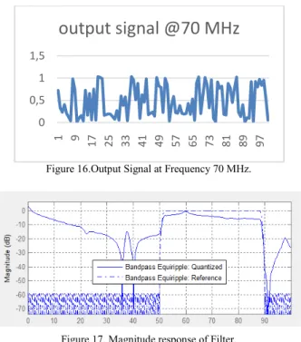
MHz , 70 MHz , 80 MHz , 90 MHz , and 100 MHz could be seen in Figure 17.
Figure 16.Output Signal at Frequency 70 MHz.
Figure 17. Magnitude response of Filter.
In Figure 17, there are two lines. The dashed line is the result of simulation and solid lines are the result of implementation. From the result, frequency response of the filter implementation has been good. Compared with the results of the simulation, bandwidth implementation results widened to 40 - 90 MHz. This happens due to several factor, such as the size of the sampling frequency used resulting order is not enough to make the filter bandwidth of 50 - 90 MHz.
Figure 18. Phase response of Filter
In Figure 18 the results of the simulation and implementation of the system is fairly linear phase response at the desired frequency range 50 - 90 MHz, this proves that the FIR filter is capable of making a linear phase response and is suitable for data communication.
CONCLUSION
In this paper, the design and realization of FIR Filter with a bandwidth of 40 MHz at 50 - 90 MHz frequency has been done.Compared with the results of the simulation, bandwidth results of the implemented filter widened to 40 - 90 MHz due to several factors such as the size of the sampling frequency used
resulting order is not enough to make the filter bandwidth of 50 - 90 MHz. Although overall, based on the results from simulation and implementation, it can be concluded that digital FIR filter designed with equiripple method can be suitable for data communication in ISL application.
ACKNOWLEDGEMENT
We would say thank you to Research Center for Electronics and Telecommunication, Indonesian Institute of Sciences (LIPI) and School of Electrical and Information Engineering, Bandung Institute of Technologies (ITB) for the financial supports and experiment facilities.
REFERENCES
[1] H. H. Kha, H. D. Tuan, T. Q. Nguyen, “An optimal design of FIR filters with discrete coefficients and image sampling application,” in Proc. of IEEE International Conference on Image Processing, 2011.
[2] H. H. Kha, H. D. Tuan, T. Q. Nguyen, “Optimal design of FIR triplet halfband filter bank and application in image coding,”
IEEE Transactions on Image Processing, 2011.
[3] C. Zhou, E. Cheng, W. Su, H. Sun, “Adaptive design of digital FIR filter for beamforming with its application in PSK UWA communication,” in Proc. of IEEE ICCA, 2010.
[4] Z. Yu-liang, W. Wei-ling, T. Bao-yu, “A novel sharp-cutoff FIR filter design technique and its application in software radio,” in Proc. of International Conference on Communication Technology Proceedings, 2003.
[5] R. Shavelis, K. Ozols, “Design of FIR decimation filters with low group delay for audio applications,” in Proc. of Biennial Baltic Electronic Conference (BEC), 2014.
[6] S.R. Kotha, D. Bilaye, U. Jain, S. S. Kumar, “An approach for efficient FIR filter design for hearing aid application,” in Proc. of International Symposium on VLSI Design and Test, 2014.
[7] N. C. Sendhilkumar, E. Logashanmugam, “Design of high speed and low power new reconfigurable fir filter for DSP applications,” in Proc. of International Conference on Current Trends in Engineering and Technology (ICCTET), 2013.
[8] A. M. Stuart lawson, Wave digital filter, 1990
[9] A. D. W. F. E. Punskaya, Particle Filtering Methods for Digital Communications, in The Telecom Handbook, 2006.
[10] R. G. Lyons, Understanding Digital Signal Processing, 2011.
0 0,5 1 1,5
1 9 17 25 33 41 49 57 65 73 81 89 97