Technology (IJRASET)
Implementation of Enhanced NOC Router
Pallavi B V1, Dr.Baswaraj Gadgay2, Veeresh Pujari3
1
PG student Dept. of VLSI Design & Embedded Systems VTU PG Centre Kalaburagi.
2
Research Guide & Professor VTU PG Centre Kalaburagi,Karnataka,India.
3
Assistant Professor VTU PG Centre Kalaburagi, Karnataka, India.
Abstract: VLSI innovation has enhanced in incorporating many cores on a single chip, but association between them is critical. NoC has appeared to be solution for this. In this paper, a novel router which is main part of on-chip network that is well suited for dynamically reconfigurable on-chip-systems is proposed. The designed router is capable of runtime detection of errors occurring while forwarding the packets since it uses error directing mechanism and it also includes self-loopback technique which enhances the performance of network by bypassing the packets when it comes to know that there is fault in the next router and it does so by checking the availability of links. It is well reasonable for the substantial movement adaptable systems and it can confine the flawed parts. Our main idea is to avoid communication failures among the nodes and hence increasing the speed of processing and maintain throughput. The source code is written in VHDL. The designed router is synthesized in XILINX ISE 12.2 and simulation is carried out by using ModelSim 10.1.
Keywords: Network on chip (NoC), Router, Loopback, VHDL.
I. INTRODUCTION
Latest innovative advancement in the area of integrated circuits has empowered designers to accommodate vast numbers of transistors. The level of incorporation has upgraded estimated power massively. The exponential decline in component size has empowered incorporation of various intellectual cores on a solitary chip prompting another era of integrated circuits called System-on-Chip. Nonetheless, as the quantity of components and their execution keep on increasing, the configuration of power, range and execution valuable communication base is increasing equivalent significance. The customary techniques for associating these heterogeneous cores are not taking care of the requests of these exceptionally compound structures. Multi processors on chip systems are developing as one of the advances giving an approach to support the developing outline multifaceted nature of integrated systems, as they give processor structures adjusted to choose issue classes, related to programming adaptability. To guarantee litheness and execution, future multi processors will combine many sorts of processor cores and information memory entity of largely distinctive sizes, prompting an exceptionally diverse design. The expanding interconnection multifaceted nature and the known versatility lack of transports want another model of interconnection.
those processors are associated together. A standout amongst the most utilized topology is the 2-Dimensional network, since it actually fits the tile-based design of the chip, and the primary segments which are employed to manufacture this are switching and processing element. It utilizes the wrapper to impart in the middle of them with the switch utilizing storage unit, decoding logic and output arbiter to make the best possible directing capability.
II. RELATED WORK
M. HOSSEINABADY et.al, [1] illustrates utilizing a large number of centers in a solitary chip are the regular pattern to manage the steadily expanding execution prerequisites of compound applications, for example, those utilized as a part of illustrations and interactive media developing. Framework on-chips in view of embedded networks on single chip are a suitable alternative for the arrangement of expansive multi core outlines with a huge number of centers. This article represents the summed up twofold de Brujin diagram as the incorporated interrelation system to impart among centers. This chart has various remarkable components that make it reasonable to execute elite, little vitality utilization, and more robust networks. EJLALI et.al, [2] illustrates design the integrated network on a single chip to withstand against high unwavering quality allied with power, superior and less vitality utilization. The effects of different blunder control designs on these goals as well as on the tradeoffs among them have been taken into account by few researches.
S. JOVANOVIC et.al, [3] illustrates the worldview for heading of data internally amid modules progressively put on a chip for reconfigurable system devices is CuNoc. Dynamism exchange of information that is generally adaptable and used for reorganized device is possible by this paradigm because of its supply correspondence unit. D. FICK et.al, [4] proposes all the other systems can adopt it by making minute changes to it and need to carry out in messaging medium. With this, it is possible to achieve changeable structure, concurrent transfer packages with related to area and also frequency.
K. SEKAR et.al, [6] proposes an integrated correspondence design as an essential determinant of general execution in complex framework on-chip outlines is introduced. Since the communiqué necessities of integrated systems can alter essentially after some time, communication models which progressively identify and adjust to such varieties can significantly improve framework execution. In this manuscript, FLEXBUS, another engineering that can productively adjust the consistent availability of the correspondence design and the parts associated with it. This design includes a progressively configurable correspondence engineering topology.
C. GRECU et.al, [7] proposes one of the upcoming methods for dealing with the difficulty of decreasing dimension of integrated multi-core chips called on chip networks is presented in this paper. Lessened element size and deep submicron impacts uncover the information transfer means of this kind of chip to large mistake rates, and extra concern should be taken to guarantee its resiliency, issue free operation. In this document, we displayed a flaw discovery design in light of a code-disjoint outline, and assessed and thought about the execution of our design and other mistake location/recuperation systems. Our discovery design can distinguish among the errors occurring in the global or local links.
C. BOBDA et.al, [8]addresses a new exemplar to hold up the communication amongst modules placed with dynamism on a reconfigurable device at runtime is described here. Adaptable communication means is addressed in this paper for on-chip network. Unlimited communication amongst processing component and pins is a permitted by designed architecture. A new steering approach is proposed which is capable of handling obstacles.
III. PROPOSED METHOD
Technology (IJRASET)
Fig-2: Block Diagram of Reliable Router
The switch is depicted by its design, includes four directions n,s,e,w suitable for a 2 dimensional networks . The processing component can be associated straightforwardly to whichever part of a switch. Even for 5 port router where the local port is committed to a processor core, this reorganization means is also applicable. The main disadvantage of this architecture is that when the permanent error occurs in common port then the processor that is connected to it is either lost or it should be removed from the chip. But in case of 4 ports router, an input can be associated with any input port and thus it can be connected strongly in the system. In addition, by utilizing dynamic partial reconfiguration and processors emphatically associated in network, none of the shortcoming area is more calamitous than any other.
Fig-3: Error in Routing Detection
A method for fault recognition is routing the data during runtime is included in this reliable switch. The XY routing algorithm can also be operated along with this method. To find the difference between the bypass of a busy element from accurate routing flaw is very complicated. If this routing flaw is not identified then there will be the possibility of packets being lost. So to identify this error made in routing depends on the slanting state indications. The basic idea of this method is that every router that receives data makes a check whether the routing made by the previous mode is correct or not. This is done after data error correction is done.
B. Diagonal Accessibility Indications
The proposed switch uses information links to indicate its adjacent node whether it is obtainable or not which is as shown in fig4. An input block which cannot receive the data is said to be busy. Our goal is to disable only flawed portions of the system so that the highest throughput can be conserved. Therefore in a router if only one portion is detected as fault then only that port can be disabled instead of entire router. If all the ports are flawed then the whole switch is said to be unavailable.
Fig- 4 : Diagonal Available Links
C. Loopback Module
In the proposed router, every port is associated with loopback section. The major task of this unit is to choose another way for the packets by circling back through some other port. Engineering of loopback part is appeared in fig 5. There are circumstances in element on chip where switches enclosing information packets in their output buffer having their adjoining hubs inaccessible because of a self-motivated re-pattern or lasting issue recognition. So in this way, these information messages stay in the yield switch until the completion of the reconfiguration or are most likely data lost, on account of identification of a perpetual broken hub. To conquer these disadvantages, these modules are actualized. It takes action only when present switch finds flaw in the next switch to which the data is to be transferred.
Technology (IJRASET)
[image:6.612.190.431.114.302.2]yield square demand, a MUX interfaces the information convey to the d_in transport.
Fig -5: Architecture of Self-Loopback Unit
Presently the logic control block arranges the semi-crossbar part to pass on the considered information on the d_loopback transport and it is reversed back within the switch .This packet is considered as another packet. So amid this progression, keeping in mind the end goal to maintain a strategic distance from the gathering of information from the neighbor, the oc_out sign is triggered. It additionally has need of one clock sequence to be traversed. This quit sending a message to that specific port from the next node at the instance of loopback.
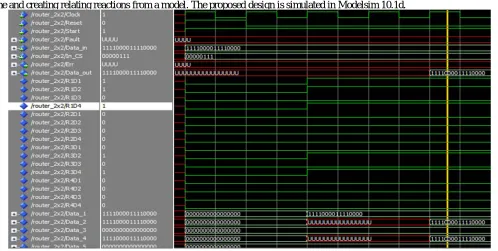
IV. SIMULATION RESULTS
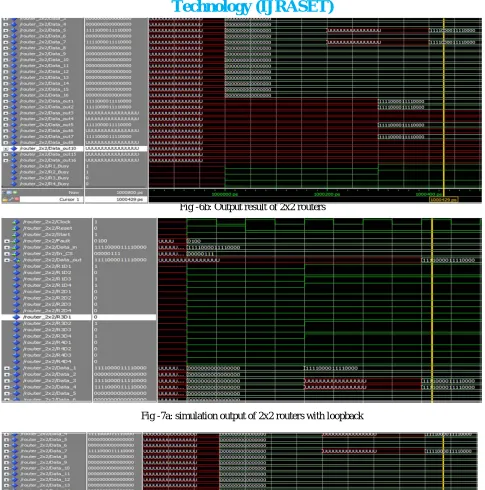
[image:6.612.52.550.441.692.2]Fig -6b: Output result of 2x2 routers
[image:7.612.59.533.491.675.2]Fig -7a: simulation output of 2x2 routers with loopback
Technology (IJRASET)
V. CONCLUSION
In this paper, a new reliable router is designed along with an error detection system that is best suited for adaptive network, which is mandatory for categorizing the flawed blocks of the system which fluctuates during execution of meticulous application. In addition a loopback segment is also added in all ports of the switch which evades the packets being blocked when it is founded that neighboring node is busy or defective .So in this way it enhances routers performance and upholds throughput. Due to the existence of error correcting schemes the repetitive exercise of logic rudiments is abridged and for that logic it is to a great extent more advantageous than common communiqué modules in a chip. The progressing work concentrates on assessing precisely the effect of defective identify blocks and enhancing the directing mislaid sighting method, by ensuring the diagonal access indication connects and steering detection section against faults.
REFERENCES
[1] M. Hosseinabady, M. Kakoee, J. Mathew, and D. Pradhan, "Low idleness and vitality productive versatile engineering for huge NoCs utilizing summed up de Bruijn chart," IEEE Trans. Large Scale Integr.(VLSI) Syst., vol. 19, no. 8, pp. 1469–1480, Aug. 2011.
[2] A. Ejlali, B. Al-Hashimi, P. Rosinger, S. Miremadi, and L. Benini, "Performability/vitality tradeoff in fault control designs for on-chip systems," IEEE Trans. Large Scale Integr. (VLSI) Syst., vol. 18, no. 2, pp. 1–14, Jan. 2010.
[3] D. Fick, A. De Orio, G. Chen, V. Bertacco, D. Sylvester, and D. Blaauw, "A profoundly strong directing calculation for issue tolerant NoCs," in Proc.Design, Autom. Test. Eur. Conf. Show., pp. 21–26, Apr 2009.
[4] S. Jovanovic, C. Tanougast, C. Bobda, and S. Weber, “CuNoC: A dynamic scalable communication structure for dynamically reconfigurable FPGAs,” Microprocess. Microsyst., vol. 33, no. 3, pp. 24–36,Feb. 2009.
[5] K. Sekar, K. Lahiri, A. Raghunathan, and S. Dey, "Powerfully configurable transport topologies for superior on-chip communicate," IEEE Trans. Large Scale Integr. (VLSI) Syst., vol. 16, no. 11, pp. 1413–1426, Oct. 2008.
[6] N. Karimi, A. Alaghi, M. Sedghi, and Z. Navabi, "Online networkon-chip switch shortcoming identification and determination utilizing practical switchfaults," J. General Comput. Sci., vol. 13, no. 22, pp. 3716–3736, IEEE Nov.2008.
[7] C. Grecu, A. Ivanov, R. Saleh, E. Sogomonyan, and P. Pande, "On-line issue identification and area for NoC interconnects," in Proc. twelfth IEEE Int. On-Line Test. Symp., pp. 145–150,Jul.2006.