Low Power Blind Adaptive Equalizer with Word
Length Optimization Algorithm
N. Alivelu Manga
Associate Professor, Dept. of ECE CBIT , Hyderabad,
Andhra Pradesh, India.
M. Madhavi Latha
, PhDProfessor, Dept of ECE, JNTUH, Hyderabad,
Andhra Pradesh, India.
ABSTRACT
Low power VLSI is a promising area for developing advanced wireless communication systems. The optimum word length selection for each signal in algorithm is crucial for low power design. This paper proposes a scheme for Word Length Optimization (WLO) using system level parameters such as dynamic range and SNR. The Blind Adaptive Equalizer for channel equalization is optimized with the proposed technique for fixed point implementation in VHDL. Simulation is carried out in MATLAB and also VHDL. Considering IEEE 802.16 wireless broadband network and DSL cable modem standards, the results are validated for Energy per Symbol to Noise density (Es/No) values 8 dB and 12 dB. Power saving up to 34% is observed for Xilinx’s Virtex-6 FPGAs, in comparison with conventional implementation. The result shows promising direction of optimization with good scope of automation for low power wireless applications. The suitability of adopted WLO scheme in the context of High Level Synthesis (HLS) is discussed.
General Terms
Low power VLSI, communication system design, Register Transfer Level (RTL), Algorithm to RTL et. al.
Keywords
WLO VLSI, Equalization, HLS, FPGA, SNR, Accuracy, Dynamic Range;
1.
INTRODUCTION
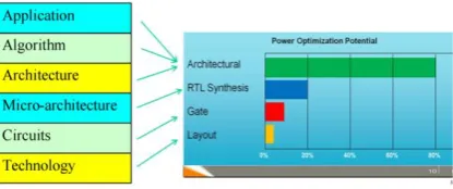
Continuous research towards low power VLSI design techniques over past few decades enabled realization of, portable communication and computing devices. Rapidly growing applications in battery powered wireless communication equipment is demanding, further power optimization of VLSI circuits. To achieve low power implementation the design, need to be optimized at all abstraction levels. To a large extent the power optimization techniques at device and circuit level are explored and are being used in present ASICs and FPGAs. The scope for power optimization at higher levels of abstraction is the new challenge in low power communication system design. The figure 1, illustrates the survey [1] results where the scope of low power is limited to 10% for Gate and Layout level techniques, where as architecture level redesign can yield 90% power optimization.
[image:1.595.323.531.243.330.2]The power optimization at higher level such as algorithm level and system level are becoming crucial in this scenario [2][3]. The reduction of power dissipation in the system context is possible by adopting suitable low power algorithms and architectures, by considering the system level specifications and performance aspects.
Fig. 1: Scope of power optimization at various abstraction levels
An attempt to dynamically adopt different scaling factors for certain category of DSP systems is described at [2]. The dynamic selection of information bits from ADC output is experimented with simulation and verified for BPSK demodulation method in [2]. The present work is continuation of this research.
The power reduction techniques in radio receiver design at higher abstraction levels considering the system level parameters are attempted by several designers in different dimensions. The work published at [4] presents a low IF based design for given signal and interference conditions. The work given at [5] discusses wake up scheme for receiver in wireless sensor network applications. However it is to be noted that, in most of the applications the required performance is well known in advance and embedding SNR estimation logic at runtime results in additional power consumption. In the proposed implementation the minimum SNR is considered as per output quality requirements and optimization is carried out based on that.
In realizing communication applications majority of the silicon is occupied by the signal processing operations which are highly computational intensive and influence the total power dissipation considerably.
Most arithmetic operations implemented on ASIC/FPGAs are based on fixed-point arithmetic representations as they occupy less area and burn less power. Whereas floating-point representation based arithmetic circuits are considerably larger and slower than their fixed-point counterparts for a given bit-width.
power optimization is possible by optimum word length selection [6][7] either in FPGAs or ASICs.
The number of bits used to represent the signal, at various stages of algorithms decides the resolution of system. In a typical communication system the bit size grows with each arithmetic operation (addition, multiplication, accumulation etc.) resulting in wider buses.
The Word Length Optimization (WLO) problem is traditionally considered as, the selection of bit widths based on the interval growths after each arithmetic operation of data path. The word length allocated at each signal stage directly affects two parameters; maximum representable value and accuracy.
The HLS approach for RTL generation is one of the emerging VLSI front end design approach, which is aimed to cut down the VLSI front end design cycle time considerably. However the optimization of generated RTL for power and speed are critical aspects for the success of the HLS based approach. The word length optimization in HLS based approach is under research from last two decades. Several approaches [8][9][10][11][12] were evolved and further optimization is under research. Existing optimization algorithms established methods for floating point to fixed point mapping under given constraints. The computation time to arrive at optimum word length is also concern in the HLS tool chain. A few recent works published towards WLO are discussed in this section. Considering all the approaches the WLO methods can be classified in to two categories.
(1) Analytical
(2) Simulation based approach
The analytical methods utilize selected analytical properties of the operations comprising the given algorithm [13]. Analytical methods usually result in more conservative word lengths, as they use worst case ranges and error models of operators in a design. They are often faster and can guarantee a lower bound for the error. However these methods directly cannot result in optimal hardware.
The simulation based methods simulate the design with a set of input stimuli and track the minimum and maximum values attained by each signal in the data path. Based on these values the suitable word length can be computed. This leads to designs that are close to the optimum [14] but no error bound can be guaranteed. If the tight word lengths are selected based on simulation, then overflows may occur. Hence usually additional few bits will be considered for deciding the worst case signal values. In algorithm transformation from DSP to ASIC [15] this is the popular method, which is used in present day word length optimization tools. The proposed method uses word length computation approach instead of simulation based, to achieve fast synthesis of data paths. Also the bit width allocation at every stage ensures with guaranteed error bounds.
The estimator presented at [8] uses Affine Arithmetic (AA) to provide a Signal-to-Quantization Noise-Ratio (SQNR) estimation for differentiable non-linear algorithms with and without feedbacks. The estimation is based on the parameterization of the statistical properties of the noise at the output of fixed-point algorithms. In paper [16], a simulation-based technique simulation-based on the relaxation of the confidence requirements of the simulations in some stages of the evaluation is presented. This work is aimed to reduce the simulation time. A WLO technique to handle constants and
variables in Linear Time Invariant (LTI) systems for given range and precision is given at [7]. However the paper doesn’t propose generalized approach to optimize the bit length against given SNR values. In this paper we propose to use processing gain measure at every stage for evolving generalized approach for bit length computation.
The paper given at [17], depicts specification of arithmetic circuits and explains the techniques for verification and bit optimization in arithmetic circuit designs. An algorithm given at [10] minimizes the hardware resources of fixed-point operations for a given accuracy constraints. The work uses weighted search algorithm, which can minimize the hardware resources for a specific FPGA by using weights.
The problem of WLO in realizing specific DSP blocks is also addressed by several researchers. The work published at [18] reduces the area for FFT implementation by varying the fixed-point length of the phase factors using phase angle error percentage as criteria. The paper at [11] exploits the Gaussian nature of OFDM signals to predict the bit-growth of the signal through the various stages of the FFT and propose a technique to scale the signal appropriately. The Sardana [12] tool optimizes the arithmetic expressions present in source codes. The optimization is done by synthesizing automatically new mathematically equal expressions, given ranges of values for the variables. The tool minimizes the number of bits required to represent without overflow the integer parts of the fixed-point numbers possibly occurring at any stage of the evaluation of an expression. However the tool do not propose any optimization criteria based on SNR values at various stages. The proposed approach with the usage of processing gains, becomes suitable for all types of DSP circuits and algorithms.
Majority of the existing proven methods can estimate optimum word length while mapping the algorithm from floating point to fixed point. The parameters considered are the worst case input and output ranges and accuracy constraints. These can be considered as first level of WLO techniques. No methods proposed so far attempt to optimize the word length based on signal characteristics and system level specifications. In communication systems this second level optimization can result in considerable area and power saving. The proposed method can achieve this by allowing graceful degradation of signal quality by reducing bit widths on the basis of minimum signal quality requirements for given application. In this paper the design optimization and results are analyzed by considering signal quality requirements for broadband wireless and cable modem applications.
The remaining part of the paper is organized into 5 sections. The section II, defines the SNR and dynamic range which are key system parameters used for optimization. The section III discusses the floating and fixed point representation along with their suitability for signal representation in communication applications. This section also discusses the bit truncation effects in this context. The section IV, describes the details of blind adaptive equalizer algorithm optimized with the proposed technique. The section V has simulation results and power analysis. The section VI concludes the paper with discussion on future possible extension.
2.
SNR AND DYNAMIC RANGE
with high dynamic range is required. Typically 80 dB dynamic range is processed in communication receivers. A practical ADC of 16 bit is used for this purpose in receiver digital front end.
As the channel is noisy, the signal available at receiver has noise energy mixed in it. In a typical receiver chain there are several stages of amplification and frequency translation. The signal to noise ratio (SNR) available at receiver decides the performance of communication system. The blocks in receiver chain either improve the SNR or reduce. Usually amplifiers, mixers and attenuators which are found in receiver front end reduce the SNR, which is accounted through noise figure. As a result, the signal at ADC output in receivers has high dynamic range (hence higher word length) but less SNR.
For a given application, the signal processing requirements demand a certain dynamic range and accuracy. The number of bits selected from ADC bits and further word lengths in every stage of processing need to consider these requirements, while achieving the optimization. This dynamic range is generally smaller than the total dynamic range offered by system. As the system is supposed to accept input right from lowest power level to highest power level, the system level dynamic range is higher.
Taking the ratio of Root Mean Square (RMS) value of full scale input to RMS value of quantization noise [19] and all other harmonics the resultant maximum Signal to noise (SNR) ratio can be given through the equation (1). Where N is the number of ADC output bits, q is the quantization Noise.
(1)
The dynamic range of a system is the ratio of the maximum signal power to minimum signal power that is of interest. The dynamic range determines the signal levels over which the receiver need to be sensitive for processing the signal. As this number is larger in value usually it is expressed in dB scale as given in equation 2.
3.
SIGNAL REPRESENTATION AND
BIT TRUNCATION
This section discusses the usage of fixed point and floating point representations in the present context. The suitable method for bit truncation is also discussed.
3.1
Fixed Point representation
The 2’s complement fixed-point arithmetic with n bits, maps the 2n combinations of binary words to integer or real numbers with equal distance on number axis. A fixed point number X with p integer bits, including one sign bit and q fractional bits and one sign bit represents decimal value as given in equation 3. The XFX represents the decimal
equivalent value of given fixed point number.
(3)
(4)
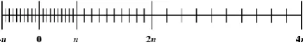
[image:3.595.323.527.317.386.2]For e.g., a 5 bit fixed point number p=3 and q=2 maps the 32 number of bit combinations to real axis as shown in Figure 2.
Fig. 2. Fixed point representation on number axis
The example represented above has dynamic range of – 4 to + 3.75, with an accuracy of 0.25. The uniform spacing of binary combinations on real axis can be observed from the Fig. 2.
3.2
Floating point representation
In case of floating point representation the step is achieved smaller (better accuracy) at lower values and larger steps at higher values. For example the IEEE 754 single precision floating point representation has 23 bit mantissa (M) and 8 bit biased exponent (E) as given in Fig. 3.
Fig. 3. IEEE 754 single precision floating point representation
Considering the E and M are integers the following equation can be used to compute the decimal equivalent of the floating point number.
(5) One can choose floating point representation with any number of bits for E and M depending on the requirement. The distribution of binary combinations in floating point with different step sizes (accuracies) can be observed in Fig. 4.
Fig.4. Real numbers in floating point representation
It is evident from the floating point arithmetic operations that it is not suitable for low power hardware implementation. To carry advantages of both fixed point and floating point scaled fixed point numbers can be used. The next section illustrates the scaling suitable for wireless receiver architecture.
3.3
Bit Truncation of Fixed Point numbers
In communication system, an Automatic Gain Control (AGC) can be used either at analog or digital level, so that the maximum signal level of instantaneous signal is mapped to a specific amplitude value. Hence signal of given dynamic range can be represented with fixed point representation. This achieves the basic advantage of floating point number representation. However the selection of number of bits in fixed point affects the quantization noise. The degradation of signal quality due to quantization noise is function of the original SNR of signal being represented. If the SNR of signal is high the truncation of least significant bits (LSBs) resulting in considerable degradation in SNR. The signal with poor1 0 0 0 0 1 0 0 0 1 1 0 0 1 0 1 0 0 1 1 1 0 1 0 0 1 0 1 0 1 1 0 1 1 0 1 0 1 1 1 1 1 0 0 0 1 1 0 0 1 1 1 0 1 0 1 1 0 1 1 1 1 1 0 0 1 1 1 0 1 1 1 1 1 0 1 1 1 1 1 0 0 0 0 0 0 0 0 0 1 0 0 0 1 0 0 0 0 1 1 0 0 1 0 0 0 0 1 0 1 0 0 1 1 0 0 0 1 1 1 0 1 0 0 0 0 1 0 0 1 0 1 0 1 0 0 1 0 1 1 0 1 1 0 0 0 1 1 0 1 0 1 1 1 0 0 1 1 1 1 -
4 - 3.7
5 - 3 .5 - 3 .2 5 -
3 - 2.7
5 - 2 .5 - 2 .2 5 -
2 - 1.7
5 - 1 .5 - 1 .2 5
-1 - 0.7
5 - 0 .5 - 0 .2 5
0 0.2
5
0
.5 0.75 1 1.25 1.5 1.75 2 5.22 2.5 2.75 3 3.25 3.5 3.75
S
E
M
[image:3.595.322.538.498.535.2]SNR, suffers less due to LSBs truncation, resulting in small SNR degradation only.
Consider a fixed point number representing scaled value ( )
which is resultant due to AGC with instantaneous gain (G). If Xi is considered as input signal with N bits before AGC, then
the scaled signal XSi is obtained by scaling such that the most
significant non-zero magnitude bits are taken. The MSB sign bit is retained as it is in this process.
6)
And the Xqi is the quantized signal resulting from quantization of least significant bits.
Fig. 5. Scaled fixed point number
The following are key advantages with receiver built with this reduced bit size.
No arithmetic units will be synthesized for manipulating the gain values at later stages. Since in most of the algorithms the relative values are important, the instantaneous gain factors can be neglected.
Implementation complexity is reduced.
The digital AGC implemented with this principle can perform dynamic bit width selection based on the detected SNR of signal.
4.
BLIND ADAPTIVE EQUALIZER
4.1
Constant Modulus based blind
equalizer
The blind adaptive channel equalizer is built with constant modulus basis is implemented here.. The algorithm in its complex form (I + jQ) is implemented here for demonstrating the principles of proposed WLO scheme. This section provides the details of implemented algorithm. The WLO is applied on the I and Q values and optimum bit widths are computed and used in the data path implementation.
The Constant Modulus Algorithm (CMA) is stochastic gradient-descent type, which adjusts the equalizer filter coefficients in the direction of the negative gradient. The algorithm can be defined as given in (7). Where μ is the step size, ∇W is the gradient with respect to the equalizer tap
coefficients, J is the cost function of the algorithm, and e(n) is the error signal of the algorithm, while (.)* denotes complex conjugation. The iterative computations of filter coefficients w(n+1) from previous cycle coefficient values w(n) is described in (7).
w(n + 1) = w(n) + μ (∇W J) (7) = w(n) + μe(n)x*(n)
As the e and x are complex, the equation will have real and imaginary components. Elaborating the (7) with real and imaginary parts results in (8).
w(n + 1) = w(n) + μ eR(n) xR(n) + μ eI(n) xI(n) + j (μ eI(n) xR(n) – μ eR(n) xI(n)) (8)
The constant modulus algorithm (CMA) [20] achieves equalization by penalizing the dispersion of the squared equalizer output modulus, |y(n)|2, from the constant C, where the CMA error is given by Equation (9) in terms of equalizer output y(n) = yR(n) + j yI(n)
e(n) = yR(n) (C – yR 2
(n) – yI 2
(n)) + j yI(n) (C – yR 2
(n) – yI 2
(n)) (9)
The filter coefficients are updated after every clock cycle as per the Equation (1). As the implementation here is pipelined, output is computed for every clock cycle. The modeling and simulation of the algorithm is given in section 5. Since the standard CMA algorithm considered here and major focus here is to apply WLO on it, detailed performance issues of CMA are not presented here.
4.2
RTL design
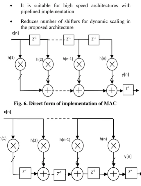
The VLSI implementation of CMA is possible in several architectural variants. Most of the ASIC and FPGA architectures are optimized to implement MAC, with one of the input vector as delayed version of input signal and filter coefficients as second vector. The Fig. 6 and 7 show two possible implementations of digital Finite Impulse Response (FIR) using MAC architecture.
The direct form of implementation, shown in Fig. 6, results from the transformation of MAC equation (2) into hardware. However its architectural variant, transposed form of MAC architecture, illustrated in Fig. 7, is usually preferred for hardware implementation because of following advantages.
It is suitable for high speed architectures with pipelined implementation
[image:4.595.316.559.384.704.2] Reduces number of shifters for dynamic scaling in the proposed architecture
Fig. 6. Direct form of implementation of MAC
Fig. 7. Transposed form of implementation of MAC
In the context of CMA algorithm the filter coefficients are computed for each clock cycle as per the equation. fixed point numbers which are already selected based on standard floating to fixed point rules. The technique presented here is Scaled Fixed point bits Truncated LSBs
Sign bit
h(1)
Z-1
h(2)
Z-1
h(n-1) h(n)
Z-1
x[n]
y[n]
Z-1
h(1)
Z-1
h(2)
Z-1
h(n-1) h(n)
Z-1
x[n]
y[n]
to evolve area and power optimized MAC implementation with SFXP representation. The modified architecture for MAC with SFXP is given at Fig. 8.
Fig.8. Transposed form of implementation of blind adaptive equalizer
In the block diagram Z-1 denotes the clocked register stages,
which are added to improve the throughput with pipelining approach.
4.3
Optimal bit width selection
The SNR and dynamic range characteristics change at every stage, due to the processing gains offered by each stage [21]. Bit width computation algorithm must consider the SNR and dynamic range as variable parameters, while selecting the word lengths.
The proposed approach uses signal to quantization noise ratio (SQNR) as the basic metric to decide the required number of bits at each signal stage. Based on the expected target signal quality at the output, the algorithm back traverses from output stage to each node to compute SQNR and hence word length. The node contribution to the increase or decrease in SQNR is pre-computed in the form of gains. From the SQNR values at each stage the word length are computed. The iterative computations of SQNR and word length at ith stage are given at (10) and (11). The SQNR2BIT can be coded by computing the N value and rounding it to next higher integer.
SQNRi = SQNRi+1 – PGi (10) WLi = SQNR2BIT(SQNRi) (11)
5.
SIMULATION AND SYNTHESIS
RESULTS
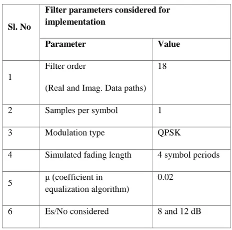
[image:5.595.46.283.111.275.2]The Table I, has the parameters considered for simulation and RTL implementation. The minimum Es/No requirement as per 802.16 broadband wireless [23] standards with forward error correction (FEC) rate of 3/4 is 8 dB. The minimum Es/No requirement for Digital Subscriber Line (DSL) standard without FEC is 12 dB. Considering these two applications the power optimization is compared at these two Es/No values.
Table I. Parameters considered for channel equalization
Sl. No
Filter parameters considered for implementation
Parameter Value
1
Filter order
(Real and Imag. Data paths) 18
2 Samples per symbol 1
3 Modulation type QPSK
4 Simulated fading length 4 symbol periods
5 μ (coefficient in equalization algorithm)
0.02
6 Es/No considered 8 and 12 dB
Since the energy per symbol rate to noise spectral density is suitable for connecting with symbol or bit error rates, in simulation this parameter is considered for noise generation. The MATLAB simulation of algorithm in the first stage is carried out for the entire algorithm and results are observed. The Fig. 9, and Fig 10 has results for Es/No =12 dB condition and Es/No = 8 dB condition respectively. The (a) is the input signal’s constellation to the blind equalizer. The part (b) is the output equalized signal constellation. The part (c) is the error in the adaptive equalization algorithm. It equalized signal can be observed in both cases. The algorithm is able to equalize the within 10000 clock cycles.
The VHDL code implemented for given architecture is simulated using Xilinx system generator (XSG) tool and results are observed through SIMULINK plots. The QPSK constellation for ideal input signal, modified with multichannel fading are shown in Figure 11(a) and 11(b) respectively. The fading is modeled for 4 symbol length using FIR filter with random coefficients. The Figure 11(c) and 11(d) show the constellations before and after equalization for Es/No value of 8 dB. The input to the algorithm 11(c) has the fading and noise added to it. The AWGN noise is added to these faded symbols to create a signal with desired Es/No level.
The Xilinx synthesis tools are used to compare the area and power of both the implemented architectures, with the general implementation. The Virtex-6 Lx240T family FPGA is selected for synthesis. The Table II, has the obtained results. To allow finer comparison the slices and DSP48 units are separately listed. It can be observed from table, when the input Es/No is 8 dB, the word lengths in the total data path are reduced, which results in speed and power optimized implementation. As the arithmetic units run faster for reduced word lengths the clock speed increases. As a result the throughput is increased by a factor of 152%. The power is saved by 34% in comparison with general implementation.
h(1)
Z-1 h(2)
Z-1
h(n-1) h(n)
Z-1
x[n]
y[n]
Z-1 COEF
update
Errror Est COEF
update
COEF update
COEF update
Fig.9.Results obtained for Es/No = 12 dB Fig.10.Results obtained for Es/No = 8 dB
(a) Input signal constellation (I-In-phase; Q-Quad-phase)
(a) Output signal constellation (I-In-phase; Q-Quad-phase)
(c) Error term in Equalization algorithm
(a) Input signal constellation (I-In-phase; Q-Quad-phase)
(b) Output signal constellation (I-In-phase; Q-Quad-phase)
(c) Error term in Equalization algorithm Digital sample index
For general implementation data-paths with 12 bit input are considered. The resulting symbol error rate at Es/No = 8 dB is observed to be 13e-4, which is comparable to the ideal SER[22] possible 12e-4.
TABLE 2. Performance, Resource usage and power comparison
Signal condition
Resource and power comparison
Parameter value comparison
Without optimization
Maximum sample rate
17 Msps --
Area - slices 3605 --
Area – DSP48
200 --
Power 636 mW --
Word length optimized for Es/No = 12 dB
Maximum sample rate
23 Msps 35% improvement in speed Area - slices 2804 22% saving
Area – DSP48
178 11% saving
Power 560 mW 12% saving
Word length optimized for Es/No = 8 dB
Maximum sample rate
43 Msps 152% improvement in speed Area - slices 1698 52% saving
Area – DSP48
124 38% saving
Power 419 mW 34%
(a)Ideal input QPSK constellation
(b) QPSK constellation effected with Multipath fading.
(c) Constellation before equalization – effected with fading and noise
[image:7.595.53.284.138.755.2](d) Constellation after equalization (output)
Fig. 11. VHDL simulation results in Xilinx System Generator (XSG) for Es/No = 8 dB
The input constellation given at figure 11(a), shows input ideal QPSK signal’s constellation with amplitudes ±0.707 + j ±0.707. After passing the signal through the multipath fading model the resulting constellation is given at figure 11(b). The signal further affected with Additive White Gaussian Noise (AWGN) is applied to the equalizer which is shown at figure 11(c). The XSG performs simulation of the equalizer block with this input and the output of the equalizer is given at figure 11(d). The results demonstrate the recovery of the QPSK constellation. The spread in constellation points expected with the presence of AWGN and also matching with MATLAB simulation results figure 10(b).
6.
CONCLUSIONS
The signal representation schemes with different binary representations are presented. The scope of word length optimization in the context communication applications, with given dynamic range and SNR is explained. A word length optimization algorithm based on acceptable SQNR is discussed.
7.
ACKNOWLEDGMENTS
Our thanks to the research review committee members and staff of ECE department, JNTU Hyderabad, for their support and suggestions.
8.
REFERENCES
[1] David Maliniak, “Designing For Low Power? Get Started At System Level”, Electronic Design, Feb 2010
[2] N. Alivelu Manga; M. Madhavi Latha, "An optimum ADC output word length selection for low power communication architectures," Advances in Computing, Communications and Informatics (ICACCI), 2013 International Conference on , vol., no., pp.569,574, 22-25 Aug. 2013, doi: 10.1109/ ICACCI.2013. 6637235.
[3] Peiyi Zhao, “Low power design of vlsi circuits and systems”, IEEE 8th International Conference on ASIC, 2009. (ASICON '09), pp: 17-20
[4] Satyam Dwivedi, Bharadwaj Amrutur and Navakanta Bhat, “Power Scalable Radio Receiver Design Based on Signal and interference condition”, Journal Low Power Electron. Appl. 2012, 2,242-264; doi:10.3390 / jlpea2040242, ISSN2079-9268
[5] Nikita Patel, Satyajit Anand and P P Bhattacharya. Article: Design of Low Power Wake-up Receiver for Wireless Sensor Network. International Journal of Computer Applications 90(10):20-25, March 2014. Published by Foundation of Computer Science, New York, USA.
[6] Jameel Hussein, Matt Klein, and Michael Hart, “Lowering Power at 28nm with Xilinx 7Series FPGAs”, White paper, WP389 (v1.1.1) February 17, 2012 available at www.xilinx.com
[7] Moni, D.J.; Sophia, P.E., "Design of low power and high speed conFigurable booth multiplier," Electronics Computer Technology (ICECT), 2011 3rd International Conference on , vol.6, no., pp.338,342, 8-10 April 2011, IEEE, doi: 10.1109/ICECTECH.2011.5942111
[8] Sarbishei, O.; Radecka, K.; Zilic, Z., "Analytical Optimization of Bit-Widths in Fixed-Point LTI Systems," Computer-Aided Design of Integrated Circuits and Systems, IEEE Transactions on , vol.31, no.3,
pp.343,355, March 2012, doi:
10.1109/TCAD.2011.2170988
[9] Caffarena, G.; Carreras, C.; Lopez, J.A.; Fernandez, A., "Fast fixed-point optimization of DSP algorithms," VLSI System on Chip Conference (VLSI-SoC), 2010 18th IEEE/IFIP , vol., no., pp.195,200, 27-29 Sept. 2010, doi: 10.1109/VLSISOC.2010.5642659
[10]Ozdil, O.; Ispir, M.; Onat, E.; Yildirim, A., "Automated fixed-point precision optimization," Signal Processing and Communications Applications Conference (SIU), 2012 20th , vol., no., pp.1,4, 18-20 April 2012, doi: 10.1109/SIU.2012.6204532
[11]Ramakrishnan, S.; Balakrishnan, J.; Ramasubramanian, K., "Exploiting signal and noise statistics for fixed point FFT design optimization in OFDM systems," Communications (NCC), 2010 National Conference on , vol., no., pp.1,5, 29-31 Jan. 2010, doi: 10.1109/NCC.2010.5430229
[12] H.-N. Nguyen, D. Menard and O. Sentieys, “Novel algorithms for word length optimization”, European Association for Signal Processing (EURASIP), 2011 - ISSN 2076-1465
[13] Gabriel Caffarena Fernández, Combined word length allocation and high level synthesis of digital signal processing circuits, Ph.D. Thesis 2008, GABRIEL CAFFARENA FERNÁNDEZ , INGENIERO DE TELECOMUNICACIÓN.
[14] Constantinides, G.A., "Perturbation analysis for word-length optimization," Field-Programmable Custom Computing Machines, 2003. FCCM 2003. 11th Annual IEEE Symposium on , vol., no., pp.81,90, 9-11 April 2003 doi: 10.1109/FPGA.2003.1227244
[15] Tor M. Aamodt and Paul Chow, “Compile-time and instruction-set methods for improving floating- to fixed-point conversion accuracy”, Article No. 26, ACM Transactions on Embedded Computing Systems (TECS), Volume 7 Issue 3, April 2008, ISSN: 1539-9087 EISSN: 1558-3465 doi>10.1145/ 1347375.1347379
[16] Sedano, E.; Lopez, J.A.; Carreras, C., "Acceleration of Monte-Carlo simulation-based quantization of DSP systems," Systems, Signals and Image Processing (IWSSIP), 2012 19th International Conference on , vol., no., pp.189,192, 11-13 April 2012
[17] Yu Pang; Sarbishei, O.; Radecka, K.; Zilic, Z., "Challenges in verifying and optimizing fixed-point arithmetic-intensive designs," Automation Quality and Testing Robotics (AQTR), 2010 IEEE International Conference on , vol.2, no., pp.1,6, 28-30 May 2010, doi: 10.1109/AQTR.2010.5520840
[18] Schmuland, T.E.; Jamali, M.M.; Longbrake, M.B.; Buxa, P.E., "Optimize hardware with fixed-point variable length phase factors," New Circuits and Systems Conference (NEWCAS), 2012 IEEE 10th International , vol., no., pp.113,116, 17-20 June 2012, doi: 10.1109/NEWCAS.2012.6328969
[19] Walt Kester, “Taking the Mystery out of the Infamous Formula, "SNR = 6.02N + 1.76dB," and Why You Should Care”, Analog Devices Tutorial, MT-001 Rev.A, 10/08, WK.
[20] Amin Mohamed Nassar and Waleed El Nahal, Blind Equalization Technique for Cross Correlation Constant Modulus Algorithm (CC-CMA), ACM WSEAS Transactions on Signal Processing archive Volume 6 Issue 2, April 2010 , Pages 23-32, ISSN:1790-5022
[21] George Constantinides, Peter Y.K. Cheung and Wayne Luk, “Synthesis and Optimization of DSP Algorithms”, Springer, 2004, ISBN 1402079303, 9781402079306.
[22] John R. Barry, Edward A. Lee and David G. Messerschmitt, Digital Communication , 3rd Edition, ISBN-13: 978-0792375487, Springer, P 184 – 194,
[23] Darcy Poulin (SiGe Semiconductor), Paul Piggin (Cygnus Communications), Ran Yaniv (Alvarion), Dov Andelman (Intel) “Correction to Rx SNR, Rx sensitivity, and Tx Relative Constellation Error for broad band wireless networks”, http://ieee802.org/16.