High Performance Implementation of Universal Gate
using Low Power Source Gating Technique
Harmeet Singh Arora
Department of Electronics and Communication Maharaja Surajmal Institute of
Technology New Delhi, India
Rohan Kochar
Department of Electronics and Communication Maharaja Surajmal Institute of
Technology New Delhi, India
Geetanjali Sharma
Department of Electronics and Communication Maharaja Surajmal Institute of
Technology New Delhi, India
ABSTRACT
Area, Speed and Cost were used to be the main concerns in the VLSI industry and Power consumption was the secondary consideration. But, nowadays, Power is given equal importance as area and speed. The increasing demand for mobile electronic devices which require complex functionality and high speed has increased the requirement for power efficient VLSI circuits. Since, a large number of transistors are being packed onto a single chip, the increase in operating frequency and processing capacity results in increased power dissipation. Power dissipation plays an important role in VLSI circuits since it not only causes overheating which reduces chip life but also makes it difficult to use devices in a portable environment [1]. Also, it results in waste of energy in form of heat which is obviously a major concern nowadays.
General Terms
Standby Power Dissipation, Active Power Dissipation, Power Analysis, NAND Gate, Sub-threshold Leakage.
Keywords
Transistor Gating, Drain Gating, Power Gating, Low Power Source Gating, Power Dissipation, Source of Power Dissipation.
1.
INTRODUCTION
Power dissipation in digital circuits is a cause of concern as it reduces the chip life and efficiency of the circuits as a result of overheating of circuit [1]. Thus, there is a need to reduce the power dissipation as much as possible. In this paper a study has been done on the effects of various previously implemented power reduction techniques on a NAND gate and also a new and improved technique has been introduced for the same purpose. There are presently 3 power reduction techniques which are: Power Gating, Drain Gating and Transistor Gating [2]. In all of these techniques the objective is to reduce the power dissipated by the circuit when it is in standby mode.
The leakage or static power dissipation, which is the power dissipated by the circuit when it is in standby mode is given by:
Pleak=Ileak*VDD (1)
where Ileak is the leakage current which flows when the circuit
is OFF and VDD is the supply voltage [2].
In all of the above mentioned techniques, the aim is to reduce this leakage current Ileak by adding extra (sleep) transistors in
the circuit in the path between power supply (VDD) and
ground. These extra transistors are inserted in such a way that the path between power supply and ground is cut-off, so that no leakage current occurs, thereby eliminating standby power dissipation.
In addition to these existing power reduction techniques, a new technique (Low Power Source Gating) has been introduced to reduce standby/leakage power. Subsequently, standby power is computed for a conventional CMOS NAND gate, NAND gate implemented using the existing techniques and also for NAND gate implemented using the proposed technique at various voltages viz. 0.5V, 0.7V, 0.8V, 0.9V and 1V. This data is compiled in a tabular form and a graph between the various voltages and the corresponding standby power dissipation is plotted. The table and graph reflect that in all the techniques as well as conventional CMOS NAND gate, standby power dissipation is directly proportional to voltage i.e. with an increase in voltage, standby power dissipation increases which is also evident from (1). Moreover, the graph depicts significantly lower power dissipation (standby) in the proposed design as compared to the power dissipation in the conventional CMOS NAND gate as well as other existing power reduction techniques.
2.
NAND GATE
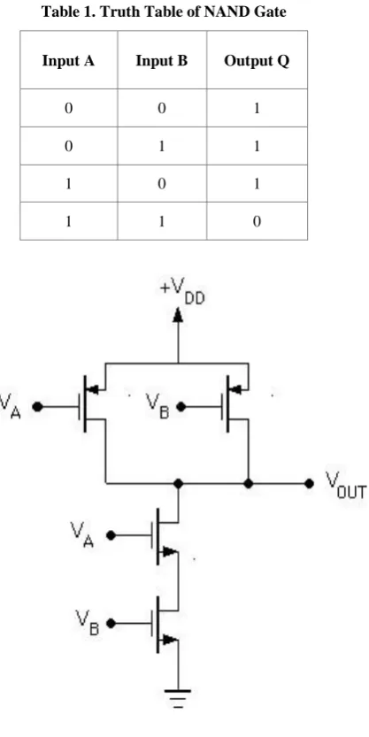
In digital circuits, a NAND gate (also known as NOT AND) is a logical gate which produces a logic 0 (or logic low) when all of its inputs are logic 1 (or logic high).If any input is logic 0 then its output will be logic 1. Thus, its output is simply a complement of the output of an AND gate. The truth table of NAND gate is shown in Table 1. The logic symbol of NAND gate is shown in Figure 1.
NAND gate is a universal gate since any Boolean function can be implemented by using a combination of NAND gates. This property is known as Functional completeness. Digital circuits implementing certain logics take advantage of NAND’s functional completeness. The CMOS NAND gate is shown in Figure 2.
Table 1. Truth Table of NAND Gate
Input A Input B Output Q
0 0 1
0 1 1
1 0 1
1 1 0
Fig 2: CMOS NAND Gate
3.
POWER DISSIPATION
3.1
SOURCE OF POWER DISSIPATION
Power dissipation is the most important aspect of digital circuits. In high performance VLSI circuits, since power dissipation is directly related to battery life, stability, performance and reliability of the circuits, therefore it is an essential requirement to reduce the power consumption as well as power dissipation.
There are three major sources of power dissipation in digital CMOS circuits: Logic transitions, Short circuit currents and Leakage currents [3].
Logic transition involves transition of nodes back and forth between the two logic levels resulting in charging and discharging of parasitic capacitances. The current flows through the channel resistance of transistors and electrical energy is converted into heat and dissipated away. Mostly, the voltage swing is equal to the supply voltage and the power dissipation due to transitions varies as the square of supply voltage [3].
Power dissipation due to short circuit currents involves flow of current directly from supply to ground when both the
Pull-Up Network and the Pull-Down Network of a complementary CMOS gate conduct simultaneously. Though, with input(s) to gate stability at their logic levels, only one of the two network conduct at a time, but when the output of a gate changes in response to change in input(s), both the networks conduct simultaneously for a very short period of time. Thus, a short circuit current flows from supply to ground through the two networks causing power dissipation [3].
The last source of power dissipation is the leakage current which flows when there is no change in input and thus no change in output of a gate. This is commonly known as static power dissipation or leakage power dissipation [3].
3.2
STANDBY POWER DISSIPATION
There are 2 modes of power dissipation modes in VLSI circuits viz. active and standby. The active mode power dissipation consists of both static and dynamic portions whereas the standby mode of power dissipation is caused by standby leakage current. Moreover, dynamic power dissipation further includes 2 components: switching power which is a consequence of charging and discharging of load capacitance and the short circuit power caused by rise and fall times of the associated waveforms. In this article, the focus is on the standby power dissipation in digital circuits.
Standby power dissipation [4], [5] is a consequence of leakage current which flows in the path between power supply and ground when the circuit is in OFF state. There are basically 4 sources of leakage current in a conventional CMOS transistor [4]:
1. Reverse-biased junction leakage current 2. Gate induced drain leakage
3. Gate direct-tunneling leakage
4. Sub-threshold (weak inversion) leakage
Out of these, the most dominant component which contributes maximum to the total leakage in CMOS circuits is the sub-threshold leakage. In this article, the sub-sub-threshold leakage has been taken into consideration. When the value of Gate to source Voltage (VGS) of a transistor is greater than its
threshold voltage (VTH), then a minority channel is created.
This is known as strong inversion. When the value of VGS of a
transistor is lower than its VTH, then there are less minority
carriers in the channel. This is known as weak inversion. Sub-threshold current of a MOSFET occurs when the Gate to source voltage (VGS)of a transistor is lower than its threshold
voltage (VTH) [4]. Thus, in CMOS design if the power supply
VDD is reduced below the threshold voltage (VTH) of a
transistor, then the circuit can be operated with sub-threshold current with ultralow power consumption. All the circuits in this article operate in sub-threshold region.
Thus, it necessitates the need for a design of a completely thorough and robust technique to reduce power dissipation in standby mode. The proposed technique is inclined towards achieving this objective with significantly greater amount of power reduction in comparison with the existing techniques.
4.
POWER REDUCTION TECHNIQUES
The power reduction techniques which are implemented on a NAND gate are:
1. Power gating 2. Drain gating 3. Transistor gating
4. Proposed technique-Low Power Source Gating In each of these techniques, extra transistors (sleep transistors) are added in the path between VDD and ground. During the
active mode (high gate input in case of NMOS and low gate input for PMOS), these sleep transistors are turned ON, which results in a reduction of resistance of the conducting path from power supply to ground, thereby avoiding performance degradation. Alternatively, during the standby mode (low gate input for NMOS and high gate input for PMOS), the sleep transistors are turned off, resulting in an increase in resistance of the conducting path which results in a subsequent and desired reduction in the leakage current and thus the leakage power [2].
4.1
POWER GATING
[image:3.595.386.476.118.336.2]In this technique, 2 sleep transistors are added, one of them between power supply and pull-up network and the other between pull-down network and ground to reduce the standby leakage current [2]. These sleep transistors are turned ON during active mode and turned OFF during standby mode, thus eliminating leakage current during standby mode as shown in Figure 3.
Fig 3: Power gating technique
4.2
DRAIN GATING
In this technique, one of the sleep transistors is added between pull-up network and circuit output and the second transistor between circuit output and pull-down network as shown in Figure 4. In active mode, these transistors are turned ON and provide a path between supply and ground whereas in standby
mode these transistors are turned OFF and break the path between supply and ground thus reducing the power dissipation in standby mode [2].
Fig 4: Drain gating technique
4.3
TRANSISTOR GATING
[image:3.595.125.219.459.666.2]This technique also involves 2 sleep transistors, one of them being added between pull-up network and circuit output and another between pull-down network and ground, with both of them aiding in leakage current minimization as in power and drain gating techniques [2]. The transistor gating technique is shown in Figure 5.
Fig 5: Transistor gating technique
4.4
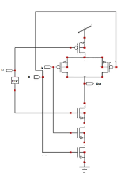
PROPOSED TECHNIQUE-LOW
POWER SOURCE GATING
[image:3.595.366.496.462.681.2]introduced in which 2 sleep transistors are inserted: first between power supply and pull-up network and the second between circuit output and pull-down network as shown in Figure 6.
[image:4.595.321.528.75.407.2]Fig 6: Proposed technique-Low Power Source Gating
Fig 8: Power gating technique
5.
IMPLEMENTATION ON NAND
GATE
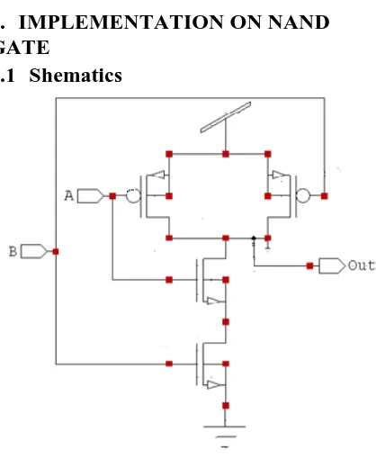
[image:4.595.114.215.140.374.2]5.1
Shematics
Fig 7: Conventional CMOS NAND Gate
[image:4.595.60.269.428.683.2]Fig 10: Transistor gating technique
Fig 11: Proposed technique-Low Power Source Gating
5.2
SIMULATION RESULTS
The results simulated for various existing low power dissipation techniques and the proposed technique were obtained on Tanner EDA Tool 13.0v over various supply voltages by using the 45nm CMOS technology. Table 2 shows active power dissipation values for conventional CMOS NAND gate, Power Gating, Drain Gating, Transistor Gating and the proposed technique- Low Power Source Gating obtained on different set of voltages. Table 3 shows the standby power dissipation for the above techniques. From
Table 3, it can be seen that the power dissipated by the proposed technique implemented NAND gate in standby mode when compared with conventional CMOS NAND gate is approximately 94% less for 1V. Similarly, the power dissipated in Low Power Source Gating technique at 1.5V, 0.9V, and 0.8V are 40.3%, 92.5% and 87% respectively less when compared to the power dissipated in conventional CMOS NAND gate. Figure 13 shows the graph between Standby Power dissipation (Watts) and Supply voltage (Volts). It can be seen that the proposed technique gives the best result when compared with other techniques as well.
Out
A
B
[image:5.595.56.259.78.626.2]Fig 12: CMOS NAND gate Simulation
Table 2. Active Power Dissipation (Watts) in various Techniques
Techniques 1.5V 1V .9V .8V .7V
CMOS 3.47E
-06 2.84E-07 1.70E-07 7.59E-08 4.15E -08 Power Gating 6.47E -06 3.63E-07 2.27E-07 1.17E-07 6.69E -08 Drain Gating 5.56E -06 4.54E-07 2.73E-07 1.46E-07 7.19E -08 Transistor Gating 5.84E -06 4.21E-07 2.71E-07 1.38E-07 7.37E -08 Proposed 6.09E
[image:5.595.321.542.199.324.2]-06 3.92E-07 2.34E-07 1.26E-07 6.61E -08
Table 3. Standby Power Dissipation (Watts) in various Techniques
Techniques 1.5V 1V .9V .8V .7V
Power Gating 2.07E-06 1.65E-08 1.31E-08 1.01E-08 7.84E-09 Drain Gating 3.05E-06 5.92E-08 3.77E-08 2.37E-08 1.47E-08 Transistor Gating 3.06E-06 6.13E-08 3.97E-08 2.53E-08 1.59E-08 Proposed
[image:5.595.66.260.338.628.2]Fig 13: Standby Power v/s Voltage
6.
CONCLUSION
In this article, the NAND gate circuits implemented by various techniques were simulated. The proposed technique dissipated less power in standby mode as compared to the conventional CMOS NAND gate as well as previously implemented techniques, i.e. Power Gating, Drain Gating and Transistor Gating. This technique is able to reduce the power dissipation in standby mode by 94 percent in NAND gate over conventional CMOS implemented NAND gate. Moreover the circuit operates in sub-threshold region which is suitable for the applications that require extremely low power consumptions.
Future work will be the implementation of the proposed technique on basic combinational circuits such as half adder,
full adder which are the nucleus of many other arithmetic operations such as subtraction, division, multiplication etc. The power dissipated by proposed technique implemented adder circuits will be compared with the power dissipated by conventional CMOS adder circuits and their power delay products will be calculated. The technique will also be implemented on domino circuits operating in sub-threshold region. The proposed technique will be useful for the self powered devices and the devices which remain active only during a portion of time and then go into sleep mode.
7.
REFERENCES
[1] S.M. Kang, Y. Leblebici “CMOS Digital Integrated Circuits analysis and design” third edition, TMH, 2003. [2] Bipin Gupta, Sangeeta Nakhate “TRANSISTOR
GATING: A Technique for Leakage Power Reduction in CMOS Circuits” ISSN 2250-2459, Volume 2, Issue 4, April 2012.
[3] M. Geetha Priya K. Baskaran D. Krishnaveni “A Novel Leakage Power Reduction Technique for CMOS VLSI Circuits” European Journal of Scientific Research ISSN 1450-216X Vol.74 No.1 (2012), pp. 96-105
[4] N.Weste and D. Harris, “CMOS VLSI Design”. Reading, MA: Addison Wesley, 2004.
[5] Z. Chen, M. Johnson, L. Wei and K. Roy, “Estimation of standby leakage power in CMOS circuit considering accurate modelling of transistor stacks,” in Proc. IEEE ISLPED, pp. 239-244, Aug. 1998.
S
tan
d
b
y
P
o
we
r
(W
att
s)