ZONE THERMAL RECRYSTALLIZATION OF THIN LAYERS FROM
A DISCRETE SOURCE
Sergei N. Chebotarev, Alexey N. Yatsenko, Vladimir N. Lozovskii, Adnan A. A. Mohamed and Georgy A. Erimeev
Platov South-Russian State Polytechnic University (NPI), Prosveshcheniya Street, Novocherkassk, Russia E-Mail: [email protected]
ABSTRACT
We have proposed and investigated a new technique for growing thin uniform layers onto a large semiconductor substrates. The method uses the system of hexagonally arranged round local sources filled with liquid growth substance. The growth substance evaporates on very close substrate, which is removed from the discrete source by about 1 mm. In these conditions vapor pressure of the residual gases is reduced by two orders of magnitude. It is found that to obtain uniform thickness layers by the proposed technique it is strongly necessary that the distance between the discrete source and the substrate will be greater than the critical thickness lcr. It is shown that this parameters lcr increases with the increasing of radius of local sources and the distance between the local sources. For example, to achieve uniformity of better than 97% the critical thickness must be equal to lcr = 1.2 mm for a hexagonal arranged system of round local sources with the radius of r = 0.75 mm and the distance between the sources of h = 0.5 mm.
Keywords: thermal recrystallization, discrete source, semiconductors, thin layers.
1. INTRODUCTION
One of the main tendencies in modern semiconductor technology is development of growth methods to produce thin layers and heterostructures on large substrates [1, 2]. Molecular-beam epitaxy is the most suitable technique to fabricate such structures [3]. Despite of the high quality of the structures, there are some drawbacks which make this method not suitable for mass production [4]. These lacks are small transfer coefficients of growth substances and active impurities, high-vacuum requirements and obtaining difficulties of uniform thickness layers on large substrates. Therefore, it is important to development growth methods, which will be free of these disadvantages. These methods are ion-beam crystallization [5-7], ion-beam sputtering [8] laser beam crystallization [9, 10] and zone sublimation regrowth [11, 12].
In the mentioned method of zone sublimation regrowth are used sublimating solid-state source and substrate, which are separated by a thin vacuum gap. Besides, the following conditions must be met:
l D
l ,
(1)
where D is the diameter of sublimating source and substrate, is the mean free path of atoms in vacuum gap. The satisfaction of the conditions (1) reduces the partial pressure of residual gases in a thin vacuum gap. This partial pressure is much lower than the pressure in the growth chamber [13]. Under the conditions of the zone sublimation regrowth, the transfer coefficients of growth substances and active impurities tend to unity. These advantages appear better for large substrates. The main disadvantage of the zone sublimation regrowth is inability to heat sublimating source above the melting temperature.
This fact limits the upper temperature limit of using the zone sublimation regrowth. For sources having very low sublimating vapor pressure, the deposition rate is very low as well. So for these materials, including 14 elements from the periodic table, the method of zone sublimation regrowth does not apply [14]. Among these 14 elements germanium is the most important for development of semiconductor devices.
The aim of this paper is to development of zone thermal recrystallization technique using a germanium discrete source for producing uniform thickness layers on large substrates. Note that the zone thermal recrystallization is the one of variation of the classical zone sublimations regrowth.
2. THEORY
of the vacuum gap after the source is divided into 5 isolated areas. It should be noted that l’’ > l’
Figure-1. Continuum source-substrate system.
If we divide the liquid layer into N isolated areas, then the overall distortion of the thickness of the vacuum gap l'' appear as a set of N separate distortions less than N
times. In this case, the minimum distance l''min is more than l'min and conglutination will not occur. As a result, a continuous source of vapor is transformed into discrete one, which can be in the liquid phase. This effect is the basis of the proposed method called the zone thermal recrystallization from a discrete source.
Figure-1 shows the ideal variant of the discrete source. A real discrete source is divided into local evaporators by mechanical barriers. Each local evaporator is filled with liquid germanium. Cross-section of the real discrete source is shown in Figure-2a. The local sources are arranged hexagonally as it one can see in Figure-2b, where 2r is the diameter of the local sources, h is the minimal distance between the neighboring local sources,
T1 and T2 are temperature of the evaporator and the substrate respectively, d is the thickness of the deposited layer.
Figure-2. Discrete source-substrate system.
The filling factor γ is one of the important characteristics. The filling factor is the ratio of the area of all local sources to the area of the wafer where the evaporators are located. The value of γ indicates how many times the flow of the evaporating material is weakened if the discrete source is used instead of a
continuous one. For example, the fill factor for circular evaporators arranged in a hexagonal is defined as
2 2 2 3 2 h r r . Figure-3 shows the layout of the local
sources.
Figure-3. The circular sources are located in a hexagonal configuration.
Obviously, the use of a discrete source generally should lead to the formation of a non-uniform layer thickness on the substrate d(x) as it can see in Figure-2. To describe this non-uniformity we use the formula from [15]. Deposition probability ω for a molecule evaporated from a circular local source to a point of the substrate, is defined as 2 2 2 2 2 2 2 2 2 4 ) ( 1 2 1 ) ( l r r l r l
, (2)
where ρ is the distance from the centre of the projection of the local source on the substrate to the point on the substrate. The layer thickness depends on the technological and geometrical parameters and is described by the equation:
k n nm z i
исп t v x d . 1 1 0 5 0
0 ( )
) ,
(
,
(3)
The central local source described by the first separate term in equation (3). The dependence of the layer thickness on temperature-time mode determined by the factor vev∙t, where vev - the rate of evaporation from the surface of each local sources, t is the time of evaporation. In the derivation of equation (3) it is assumed the additivity of molecular flows from the local sources. It does not take into account the surface diffusion and the atoms multipath from the source and substrate. These factors can lead to a weakening of the modulation of thickness deposited layer d(x,φ). The position of the point, in which is calculated d, is given by polar coordinates x
and φ. To determine the non-uniformity of the grown layer is sufficient to consider the direction, which is given by formula φ = π/6 + qπ/3 (q = 0, 1, 2, ...), for example Ox in Figure-3. Indeed, this non-uniform layer thickness is determined by two variables dmin and dmax. The parameter
dmax is measured on the substrate against the center of the local source, which is shown by the red circle in Figure-3. The value dmin is also measured on the substrate against the point, which is detected by the yellow square in Figure-3. Therefore, the extremes of the function d(x, φ)
lie on the axes φ = π/6 + qπ/3 (q = 0, 1, 2, ...).
3. MATERIALS AND METHODS
Experimental verification of the possibility of obtaining uniform thickness layers on large substrates was carried out using germanium as a model material. The evaporator is made of chemical pure finely porous graphite. The system of the local sources with geometry as it is shown in Figure-3 was drilled in the evaporator. Graphite vapor pressure at the operating temperature of the deposition process is not more than 10-9 Pa. Graphite is essentially insoluble in germanium and quite easily handled mechanically. After machining the graphite wafer was hardened by the pyrolytic carbon layer. Then this hardened wafer was thermal cleaned in a vacuum. The 100 mm standard polished silicon wafers with crystallographic orientation (100) is used as substrates. Further purification was achieved by sublimation etching of the substrate at the temperature of 1150 °C in a vacuum. The drilled local sources were loaded with germanium powder. Then the loaded germanium powder was melted. Note that the vapor pressure of liquid germanium during the deposition of the layer in the temperature range 650 to 920 °C is less than 10-2 Pa. In this experimental conditions the requirements (1) is well satisfied (l/R < 10-3, l/λ ≈ 10-4). Scanning electron microscopy were used to investigate the thickness of the grown layers using position mark technique [16]. The example of layer thickness measuring is shown in Figure-4.
Figure-4. Cross-section of the non-uniformity deposited layers.
The layer thicknesses were determined by SEM with a precision of 25 nm. The thickness of germanium layers were about 10 µm to reduce the measurement errors.
4. RESULTS AND DISCUSSIONS
The non-uniformity of the deposited layer is calculated by the formula:
max min/
1d d
, (4)
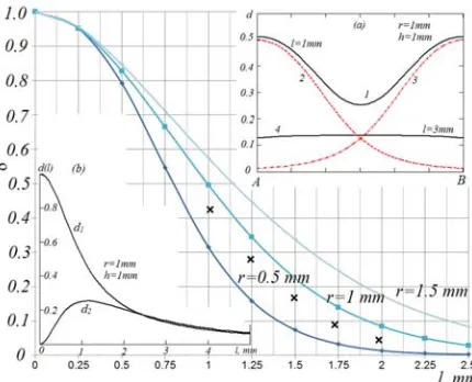
Figure-5. The dependence of non-uniformity thickness on the distance between the source and the substrate l at
different radius of the local sources r and the constant distance between local sources h = 1 mm.
Thereby the zone thermal recrystallization from a discrete source must satisfy the following three conditions:
D
l , l, llcr, (5)
where lcr is determined for each type of discrete source for a given level of non-uniformity. It should be noted that the classical method of zone sublimation regrowth must meet only two conditions defined in equation (1).
The experimental data reflected the crosses in Figure 5 support the conclusions of the theory. However, the experimental value of δ is always less than the theoretical. This can be explained by three reasons. Firstly, in our calculating the surface shape of the liquid phase was flat. Realistically, this surface has a convex shape. Secondly, in the calculation we did not consider germanium re-evaporation from the substrate. Thirdly, we did not take into account the alignment of layer thickness due to surface diffusion. Each of these factors decreases the non-uniformity that was confirmed experimentally.
4. CONCLUSIONS
The new method of zone thermal recrystallization from a discrete source to obtain uniform thin semiconductor layers was proposed. The method uses the system of geometrical arranged local sources filled with liquid growth substance. The growth substance evaporates on very close substrate, which is removed from the discrete source by about 1 mm. In these conditions vapor pressure of the residual gases is reduced by two orders of
density of local sources. For example, to achieve uniformity of better than 97% the critical thickness must
be equal to
lcr = 1.2 mm for a hexagonal arranged system of round local sources with the radius of r = 0.75 mm and the distance between sources of h = 0.5 mm.
ACKNOWLEDGMENTS
The authors would like to thank for financially supporting this work the Russian Foundation for Basic Research [grant number 15-08-08263_a]. The reported study was also funded by the Grant of the President of Russian Federation for young PhD [project MK-5115.2016.8].
REFERENCES
[1] Shengurov V.G., Chalkov V.Y., Denisov S.A., Stepikhova M.V., Krasilnik Z.F. 2016. Conditions of growth of high-quality relaxed Si1–xGex layers with a high Ge content by the vapor-phase decomposition of monogermane on a sublimating Si hot wire. Semiconductors. 50(9): 1248-1253. DOI: 10.1134/S1063782616090220.
[2] Shengurov V.G., Denisov S.A., Svetlov S.P., Chalkov V.Y., Shengurov D.V. 2016. A device for heating a substrate during molecular beam epitaxy. Instruments and Experimental Techniques. 59(2): 317-320. DOI: 10.1134/S0020441216020135.
[3] Boldyrevskii P.B., Korovin A.G., Denisov S.A., Svetlov S.P., Shengurov V.G. 2014. Thickness uniformity of silicon layers grown from a sublimation source by molecular-beam epitaxy. Technical Physics,
59(11): 1732-1735. DOI:
10.1134/S1063784214110073.
[4] Chebotarev S.N., Pashchenko A.S., Lunin L.S., Irkha V.A. 2013. Features in the formation of Ge/Si multilayer nanostructures under ion-beam-assisted crystallization. Technical Physics Letters, 39(8): 726-729. DOI: 10.1134/S1063785013080178.
Nanotechnologies in Russia, 11(7-8): 435-443. DOI: 10.1134/S1995078016040030.
[7] Chebotarev S.N., Pashchenko A.S., Williamson A., Lunin L.S., Irkha V.A., Gamidov V.A. 2015. Ion beam crystallization of InAs/GaAs(001) nanostructures. Technical Physics Letters, 41(7): 661-664. DOI: 10.1134/S1063785015070056.
[8] Chebotarev S.N., Pashchenko A.S., Irkha V.A., Lunina M.L. 2016. Morphology and Optical Investigations of InAs-QD/GaAs Heterostructures Obtained by Ion-Beam Sputtering. Journal of
Nanotechnology, 2016: 5340218. DOI:
10.1155/2016/5340218.
[9] Balandin V.Yu., Aleksandrov L.N., Dvurechenskii A.V., Kulyasova O.A. 1994. Interference effects at laser pulse heating of multilayer structures. Physica Status Solidi(a), 142(1): 99-105. DOI: 10.1002/pssa.2211420112.
[10]Lunin L.S., Chebotarev S.N., Pashchenko A.S., Dudnikov S.A. 2013. Correlation between the size and photoluminescence spectrum of quantum dots in InAs-QD/GaAs. Journal of Surface Investigation, 7(1): 36-40. DOI: 10.1134/S1027451013010138.
[11]Aleksandrov L.N., Lozovskii S.V., Knyazev S.Y. 1988. Silicon zone sublimation regrowth. Physica Status Solidi(a), 107(1): 213-223. DOI: 10.1002/pssa.2211070122.
[12]Denisov S.A., Svetlov S.P., Chalkov V.Y., Shengurov D.V., Shengurov V.G. 2015. A device for growing silicon films on standard wafers using a sublimation source. Instruments and Experimental Techniques, 58(6): 813-816. DOI: 10.1134/S0020441215050048.
[13]Lozovskii V.N., Lozovskii S.V., Valov G.V. 2013. Sorption vacuumization of a growth cell during zone sublimation recrystallization. Technical Physics
Letters. 39(2): 175-178. DOI:
10.1134/S1063785013020120.
[14]Filatov D.O., Gorshkov A.P., Volkova N.S., Denisov S.A., Shengurov V.G. 2015. Photodiodes based on self-assembled GeSi/Si(001) nanoisland arrays grown by the combined sublimation molecular-beam epitaxy of silicon and vapor-phase epitaxy of germanium. Semiconductors. 49(3): 387-393. DOI: 10.1134/S1063782615030082.
[15]Lozgachev V.I. 1962. The distribution of molecules in the plane streams by evaporation in vacuum. Technical Physics, 32(8): 1012-1022.
[16]Lozovskii V.N., Chebotarev S.N., Irkha V.A., Valov G.V. 2010. Formation and use of positioning marks in scanning probe microscopy. Technical Physics
Letters, 36(8): 737-738. DOI: